BACKGROUND OF THE INVENTION
Field of the Invention
The present invention relates to a photovoltaic
device such as a solar cell, a sensor or an imaging
device, and more particularly to a stacked
photovoltaic device having a plurality of pin
junctions stacked therein.
Related Background Art
Heretofore, for the purpose of enhancing an
efficiency of an amorphous silicon solar cell and of
reducing light degradation, there have been disclosed
many techniques concerning a stacked photovoltaic
device in which a plurality of pin elements are
joined to one another. In one of the techniques,
solar light is optically divided into a plurality of
wavelength sensitivity regions to be absorbed, to
thereby allow carriers generated through reception of
the solar light to be more efficiently utilized while
also the number of carriers generated through
reception of the solar light in each element is
reduced. Consequently, light degradation is
suppressed.
For example, as for a stacked amorphous silicon
solar cell having a three-layer structure, a device
having the three-layer structure composed of a-SiC/a-Si/a-SiGe,
a-Si/a-SiGe/a-SiGe, a-SiC/a-SiGe/a-SiGe,
or the like is proposed (refer to Japanese Patent
Application Laid-Open No. H5-102505), and an attempt
has been made for efficiently utilizing solar light.
However, in an amorphous material such as a-SiGe,
or a-Si, travelling property of carriers is
lower than that in microcrystalline silicon or
crystalline silicon. In addition, as thickness of
the amorphous material is increased, its film
characteristics are remarkably deteriorated. Hence,
there is a limit to the way of increasing a
photoelectric current density by thickening a film.
In particular, an a-SiGe-based film has a problem
that if its thickness is increased, then the
degradation becomes remarkable when light is applied
to this film.
On the other hand, in recent years, it was
disclosed by Neuchatel University that a high quality
microcrystalline silicon thin film can be formed by
utilizing the plasma CVD method (refer to U. S.
Patent No. 6,309,906), and studies regarding this
technique have been conducted in various organs.
Japanese Patent Application Laid-Open No. H11-243218
discloses a stacked photovoltaic device having
a three-layer structure composed of a-Si/µC-Si/µC-Si.
In addition, Japanese Patent Application Laid-Open
No. H11-243219 discloses a stacked photovoltaic
device in which a current value is controlled by a
constituent element including a pin junction having a
microcrystalline semiconductor material as an i layer
to thereby allow a device of a high efficiency to be
formed.
However, it was judged that the degradation of
the characteristics of microcrystalline silicon due
to the application of light is less than that of
amorphous silicon, or such degradation of the
characteristics is hardly caused. Hence, until now
there has not been disclosed at all such a technique
as to give a solution to a problem concerning what
kind of stacked structure can provide the optimal
photovoltaic characteristics in a stacked
photovoltaic device in which a plurality of i-type
semiconductor layers are formed of microcrystalline
silicon.
However, in actuality, in microcrystalline
silicon as well, it has been made clear that the film
quality and the optical degradation characteristics
greatly differ depending on formation conditions and
a thickness of microcrystalline silicon. Hence, it
is necessary to design a stacked photovoltaic device
with due consideration for the optical degradation
characteristics of microcrystalline silicon.
SUMMARY OF THE INVENTION
In the light of the foregoing, the present
invention has been made in order to solve the above-mentioned
problems associated with the prior art, and
it is, therefore, an object of the present invention
to provide a silicon-based photovoltaic device which
is capable of exhibiting a high photoelectric
conversion efficiency and of maintaining stable
characteristics for a long period of time against
application of light in a stacked photovoltaic device
including a plurality of photovoltaic devices each
having a pin junction which are stacked, in which a
plurality of i-type semiconductor layers comprise
microcrystalline silicon.
In order to attain the above object, according
to the present invention, there is provided a stacked
photovoltaic device including a plurality of
photovoltaic devices each having a pin junction
including a p-type semiconductor, an i-type
semiconductor, and an n-type semiconductor each made
of a non-single crystal having an element belonging
to the IV group as a main component and which are
stacked on a substrate, characterized in that: a
first i-type semiconductor layer comprises amorphous
silicon hydride, and second and subsequent i-type
semiconductor layers comprise amorphous silicon
hydride or microcrystalline silicon, the i-type
semiconductor layers being stacked in order from a
light incidence side; and when an open circuit
voltage is assigned Voc in the case where a pin
photoelectric single element is manufactured using a
pin element having the i-type semiconductor layer
made of microcrystalline silicon of pin elements (pin
photoelectric element having pin junction) having the
second and subsequent i-type semiconductor layers,
respectively; and a layer thickness of the i-type
semiconductor layer concerned is assigned t, a short-circuit
photoelectric current density of the stacked
photovoltaic device is controlled by the pin element
including the i-type semiconductor layer having the
largest value of Voc/t. At this time, it is
desirable that when solar light of AM1.5 is applied
to the stacked photovoltaic device under the
condition of 1SUN and at 25°C, a sum of the short-circuit
photoelectric current densities obtained from
the individual layers is equal to or larger than 27
mA/cm2. Further, it is desirable that in the
photovoltaic devices, the short-circuit photoelectric
current density of the pin element having the i-type
semiconductor layer made of amorphous silicon hydride
is larger than that of the pin element having the i-type
semiconductor layer made of microcrystalline
silicon.
BRIEF DESCRIPTION OF THE DRAWINGS.
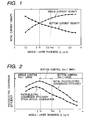
FIG. 1 is a graphical representation showing
typical experiment results useful in explaining a
relationship among Voc/t, a control element and
device characteristics in a stacked photovoltaic
device of the present invention;
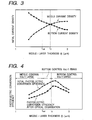
FIG. 2 is a graphical representation showing
typical experiment results useful in explaining a
relationship among Voc/t, a control element and
device characteristics in a stacked photovoltaic
device of the present invention;
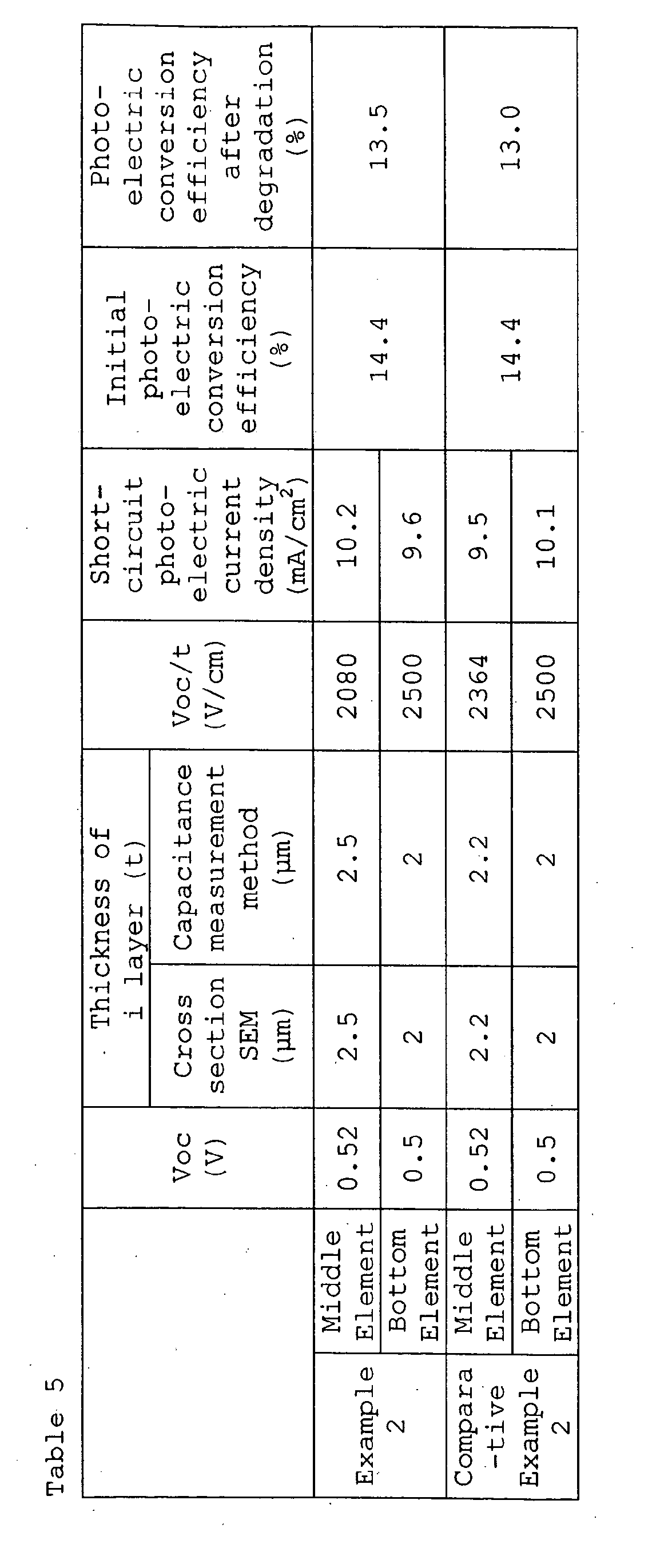
FIG. 3 is a graphical representation showing
typical experiment results useful in explaining a
relationship among Voc/t, a control element and
device characteristics in a stacked photovoltaic
device of the present invention;
FIG. 4 is a graphical representation showing
typical experiment results useful in explaining a
relationship among Voc/t, a control element and
device characteristics in a stacked photovoltaic
device of the present invention;
FIG. 5 is a schematic view showing a deposition
film forming system for forming a stacked
photovoltaic device of the present invention;
FIG. 6 is a graphical representation showing a
relationship between a total photoelectric current
density and a photoelectric conversion efficiency
after degradation of a stacked photovoltaic device;
and
FIG. 7 is a schematic view showing a form of a
layer structure of a stacked photovoltaic device of
the present invention.
DETAILED DESCRIPTION OF THE PREFERRED EMBODIMENTS
As described above, the present invention
relates to a novel stacked photovoltaic device, and
an operation of the present invention will
hereinafter be described in detail.
In a stacked photovoltaic device in which a
plurality of photovoltaic devices each having a pin
junction are joined in series with one another (for
example, the constituent elements of a triple device
are called a top element, a middle element, and a
bottom element from a light incidence side), a short-circuit
photoelectric current density of the stacked
photovoltaic device can be maximized by making
densities of short-circuit photoelectric currents
generated in the respective constituent elements
equal to one another. However, the characteristics
of the whole device has a tendency to strongly
reflect the characteristics of the constituent
element (control element) having the least
photoelectric current generated therein. Hence, an
appropriate current balance is obtained rather than
densities of short-circuit photoelectric currents
generated in the respective constituent elements are
made equal to one another, whereby the photoelectric
conversion efficiency of the whole device can be
enhanced. Consequently, even if film qualities of
the constituent elements are equal to one another,
how a control element is selected exerts a large
influence on the photoelectric conversion efficiency
of the device.
As described in Japanese Patent Application
Laid-Open No. H11-243219, since the characteristics
of the amorphous silicon photovoltaic device are
greatly degraded by application of light, it is not
preferable to set a top element as a control element
since the characteristics are further reduced after
light degradation. On the other hand, it has been
made clearer that the characteristics of a film made
of microcrystalline silicon largely differ depending
on the manufacture conditions. It is conceived that
this is because unlike a crystal, grain boundaries
are present in a microcrystal, and hence a state of
grain boundaries, a crystal grain diameter, a
microcrystallization rate and the like are changed
depending on the manufacture conditions. For this
reason, in particular, Voc when a pin photovoltaic
single device is manufactured can be largely changed
so as to fall within the range of about 0.3 to about
0.6 V. In this case, while its light degradation
rate due to application of light is small as compared
with an amorphous silicon film, its light degradation
rate is changed largely depending on a film quality
of a microcrystalline i-type semiconductor layer.
The present inventors have earnestly made a
study of this respect, and as a result, they have
found out that in a stacked photovoltaic device in
which a plurality of i-type semiconductor layers
comprise microcrystalline silicon, when a layer
thickness of the microcrystalline i-type
semiconductor layer is assigned t, a pin element
having the largest Voc/t is selected as a control
element, whereby the characteristics after light
degradation can be greatly enhanced. Voc/t is a
parameter correlating with an internal electric field.
It is conceivable that the travelling property of
carriers are further enhanced as Voc/t is increased,
and as a result, the characteristics of the whole
device can be enhanced, and also a rate of
degradation due to application of light for a long
period of time can be reduced.
Moreover, the stacked photovoltaic device of
the present invention especially shows a large effect
in a case where a sum of densities of photoelectric
currents obtained from individual pin elements when
the solar light of AM1.5 is applied to the stacked
photovoltaic device under the conditions of 1SUN,
25°C is equal to or larger than 27 mA/cm2. FIG. 6
shows a graphical representation in which for a
triple element composed of a-Si/microcrystalline
Si/microcrystalline Si, and a double element composed
of a-Si/microcrystalline Si, data of photoelectric
conversion efficiency after light degradation is
plotted against a sum of current densities obtained
from the respective elements (total photoelectric
current density). As shown in FIG. 6, it is
understood that while when the current density is
smaller than 27 mA/cm2, the photoelectric conversion
efficiency of the triple element is slightly larger
than that of the double element, when the current
density becomes larger than 27 mA/cm2, as the total
photoelectric current density is increased, the
photoelectric conversion efficiency of the triple
element becomes greatly larger than that of the
double element. As this cause, it is mainly
presumable that since a short-circuit photoelectric
current density (Jsc) of the double element is about
1.5 times as large as that of the triple element if
their film qualities are equal to each other, the
light degradation of the a-Si layer becomes abruptly
remarkable as the total photoelectric current density
is increased. From a viewpoint of a manufacture cost
as well, the raw material cost and the manufacture
time of the triple element are increased as compared
with the double element. Thus, it is judged that the
cost per output electric power of the triple element
becomes more advantageous than that of the double
element when the total photoelectric current density
is nearly equal to or larger than 27 mA/cm2.
In such a manner, the present inventors have
found out that the photoelectric conversion
efficiency of the stacked photovoltaic device
manufactured by stacking three or more layers of the
photovoltaic elements each having a pin junction is
most remarkably enhanced when the total photoelectric
current density is equal to or larger than 27 mA/cm2.
In addition, the pin element having an i-type
semiconductor layer made of amorphous silicon is more
remarkable in the characteristics degradation due to
application of light than the pin element having an
i-type semiconductor layer made of microcrystalline
silicon. Thus, the short-circuit photoelectric
current density of the pin element having an i-type
semiconductor layer made of amorphous silicon is made
larger than that of the pin element having an i-type
semiconductor layer made of microcrystalline silicon
to thereby allow the device characteristics after
light degradation to be enhanced.
Embodiments of the stacked photovoltaic device
of the present invention will hereinafter be
described in detail with reference to the
accompanying drawings. It should be noted that the
present invention is not intended to be limited to
these embodiments.
FIG. 7 is a schematic view showing a form of a
layer structure of a stacked photovoltaic device of
the present invention. The stacked photovoltaic
device shown in FIG. 7 has a layer structure in which
a collector electrode 401 made of metal such as Ag, a
transparent and electroconductive antireflection
layer 402 made of indium oxide, tin oxide, or the
like, a first p(n)-type semiconductor layer 403, a
first i-type semiconductor layer 404, a first n(p)-type
semiconductor layer 405, a second p(n)-type
semiconductor layer 406, a second i-type
semiconductor layer 407, a second n(p)-type
semiconductor layer 408, a third p(n)-type
semiconductor layer 409, a third i-type semiconductor
layer 410, a third n(p)-type semiconductor layer 411,
a reflection enhancing layer 412 made of zinc oxide,
indium oxide, tin oxide, or the like, and a
reflecting layer 413 made of Al, Cu, Ag, etc. are
formed in this order from a light incidence side on a
substrate 414 such as a metallic substrate made of
stainless steel, or an insulating substrate made of
glass. In addition, the elements each composed of a
pin structure are called a top element 415, a middle
element 416, and a bottom element 417, respectively,
from the light incidence side.
FIG. 1 is a graphical representation showing a
change in short-circuit photoelectric current
densities of the middle element and the bottom
element when the triple element having an i layer of
the top element made of amorphous silicon hydride,
and i layers of the middle element and the bottom
element made of microcrystalline silicon is
manufactured while changing a thickness (assigned t)
of the i-type semiconductor layer of the middle
element. At this time, the manufacture conditions of
the top element and the bottom element are made fixed,
and the condition is selected such that when each of
the bottom element and the middle element is
manufactured in the form of a single element, the
same Voc is obtained. In FIG. 1, t
bot represents a
layer thickness of the i-type semiconductor layer of
the bottom element, and t
0 represents a layer
thickness of the i-type semiconductor layer of the
middle element at which the short-circuit
photoelectric current densities of the bottom element
and the middle element become equal to each other.
As a result, for layer thickness areas of the i layer
of the middle element, a relationship between the
control element and Voc/t is expressed as shown in
Table 1.
FIG. 2 is a graphical representation showing a
relationship between an initial photoelectric
conversion efficiency, and a photoelectric conversion
efficiency after degradation since the photovoltaic
device is optically degraded due to light application
at 1SUN, 50°C for 1,000 hours the data of which is
plotted against a thickness (t) of the i layer of the
middle element. From FIG. 2, it is understood that
in an area of t < t0 and an area of t0 < t < tbot, a
device fulfilling the area of t < t0 of devices
having nearly the same initial photoelectric
conversion efficiency shows a higher photoelectric
conversion efficiency after degradation. Moreover,
it is understood that in a triple element having the
maximum photoelectric conversion efficiency after
degradation, in case of the area of t < t0, a middle
element having a larger value of Voc/t becomes a
control element. That is to say, it is shown that
the adjustment is made so that an element having a
larger value of Voc/t becomes a control element,
whereby the photoelectric conversion efficiency after
degradation is enhanced. Note that, though in an
area of t > tbot, the light degradation is not
remarkable, since the initial photoelectric
conversion efficiency is extremely reduced, no high
efficiency is expected.
Likewise, in FIG. 3, short-circuit
photoelectric current densities of a bottom element
and a middle element when tbot is smaller than t0 are
shown as a function of a thickness (t) of an i layer
of the middle element. Hence, for setting tbot to be
smaller than t0, various methods are available. For
example, when a reflection enhancing film having a
high texture degree, since a current of a bottom
element can be mainly increased by reflected light
from a rear face, it is possible to decrease a layer
thickness of an i layer of the bottom element. In
other words, since incident light is absorbed from
the i-type semiconductor layer on a light incidence
side, a quantity of incident light is successively
decreased after passing through the top element, the
middle element, and the bottom element in this order.
However, in the bottom element, an increase in
quantity of current due to the reflected light is
anticipated. For this reason, a magnitude
relationship between the photoelectric current
densities of the middle element and the bottom
element is changed depending on not only layer
thicknesses and film qualities of the i layer of the
middle element and the i layer of the bottom element,
but also a reflectivity and a reflection angle of the
reflection enhancing film. These parameters are
controlled to allow magnitudes of Voc/t of the
elements to be changed.
From FIG. 3, for the areas of layer thickness
the of the i layer of the middle element, a
relationship between the control element and Voc/t is
expressed as shown in Table 2.
FIG. 4 is a graphical representation showing a
relationship between an initial photoelectric
conversion efficiency, and a photoelectric conversion
efficiency after degradation since the photovoltaic
device is optically degraded due to light application
at 1SUN, 50°C for 1,000 hours the data of which is
plotted against a thickness (t) of the i layer of the
middle element. From FIG. 4, it is understood that
in an area of tbot < t < t0 and an area of t > t0, a
device fulfilling the area of t > t0 of devices
having nearly the same initial photoelectric
conversion efficiency shows a higher photoelectric
conversion efficiency after degradation. Moreover,
it is understood that in a triple element having the
maximum photoelectric conversion efficiency after
degradation, in case of the area of t > t0, a bottom
element having a larger value of Voc/t becomes a
control element. In this case as well, it is shown
that by setting an element having a larger value of
Voc/t as a control element, the photoelectric
conversion efficiency after degradation is enhanced.
Note that, though in an area of t < tbot, the light
degradation is not remarkable, since the initial
photoelectric conversion efficiency is extremely
reduced, no high efficiency is expected.
The above-mentioned experiments were made with
respect to a case where Voc of the middle element is
equal to that of the bottom element. However, it has
been found out that in a case as well where Voc of
the middle element is different from that of the
bottom element, likewise, the adjustment is made so
that the element having the larger value of Voc/t
becomes the control element, whereby it is possible
to maximize the photoelectric conversion efficiency
after degradation.
Thus, it has become clear that for enhancing
the efficiency of the stacked photovoltaic device
having a plurality of i-type semiconductor layers
each made of microcrystalline silicon, it is
important that before the light degradation, in a
state in which the short-circuit photoelectric
current densities of the constituent elements are
close to one another, the pin element including a i-type
semiconductor layer made of microcrystalline
silicon and having the largest value of Voc/t is set
as the control element. Such a relationship is also
applied to a stacked photovoltaic device in which
four or more layers of photovoltaic devices each
having a pin junction are stacked.
Next, a measurement method and a manufacturing
system which are applied to the present invention
will hereinafter be described in detail.
(Measurement of Short-Circuit Photoelectric Current)
The short-circuit photoelectric current
densities of the constituent elements of the stacked
photovoltaic device are measured on the basis of the
spectral sensitivity characteristics of elements.
For example, in case of a three-layer stacked
photovoltaic device in which three photovoltaic
devices each having a pin junction are stacked in
series with one another, the short-circuit
photoelectric currents of a top element, a middle
element, and a bottom element, for example, are
measured in accordance with the following manner.
The measurement of the short-circuit
photoelectric current density of the top element is
carried out as follows. A forward bias voltage is
applied which corresponds to a sum of electrovoltaic
voltages which are generated in the middle element
and the bottom element, respectively, when light is
applied to the stacked photovoltaic device, and light
in the regions in which the light is mainly absorbed
by the middle element and the bottom element is
applied in the form of bias light. Then, light
spectrally separated in this state is applied to
measure the spectral characteristics, and the
resultant spectral characteristics are multiplied by
the spectral intensity of solar light to calculate
the short-circuit photoelectric current density of
the top element.
For the measurement of the short-circuit
photoelectric current density of the middle element,
similarly to the case of the top element, a forward
bias voltage is applied corresponding to a sum of
electrovoltaic voltages generated in the top element
and the bottom element, respectively, and light in
the regions which the light is mainly absorbed in the
top element and the bottom element, respectively, is
applied in the form of bias light. Then, light
spectrally separated in this state is applied to
measure the spectral characteristics, and the
resultant spectral characteristics are then
multiplied by the spectral intensity of solar light
to calculate the short-circuit photoelectric current
density of the middle element.
For the measurement of the short-circuit
photoelectric current density of the bottom element,
likewise, a forward bias voltage is applied
corresponding to a sum of electrovoltaic voltages
generated in the top element and the middle element,
respectively, and light in the regions in which the
light is mainly absorbed in the top element and the
middle element, respectively, is applied in the form
of bias light. Then, light spectrally separated in
this state is applied to measure the spectral
characteristics, and the resultant spectral
characteristics are then multiplied by the spectral
intensity of solar light to calculate the short-circuit
photoelectric current density of the bottom
element.
(With Respect to Voc in the Present Invention)
Essentially, it is preferable that Voc of each
of the single elements is calculated with respect to
each of the manufactured single elements. However,
in the present invention, for example, the following
evaluation method can be substituted for the
evaluation for Voc of each of the single elements in
the stacked photovoltaic device.
For example, Voc of a bottom element in a
triple element is defined as follows. In the above-mentioned
method that includes measuring the short-circuit
photoelectric current densities, a wavelength
of the spectrally separated light is fixed to a
wavelength at which the highest quantum efficiency is
obtained in a bottom element, and an applied bias
voltage is then increased from 0V. Then, the forward
bias voltage value when the quantum efficiency is
reduced by 1.5% from the case of the applied bias
voltage of 0 V is measured. A voltage which is
obtained by subtracting the resultant forward bias
voltage from Voc which is obtained by applying light
of 1SUN and AM1.5 is defined as Voc of the bottom
element.
Likewise, in a top element as well, in the
above-mentioned method including measuring the short-circuit
photoelectric current density, a wavelength
of the spectrally separated light is fixed to a
wavelength at which the highest quantum efficiency is
obtained in the top element, and an applied bias
voltage is then increased from 0V. Then, the forward
bias voltage value when the quantum efficiency is
reduced by 1.5% from the case of the applied bias
voltage of 0 V is measured. A value which is
obtained by subtracting the resultant forward bias
voltage value from Voc of the triple element is
defined as Voc of the top element.
Voc of a middle element is similarly defined.
However, in case of an element sandwiched between
upper and lower elements as in the middle element, a
wavelength of the spectrally separated light is fixed
to a wavelength at which the highest quantum
efficiency is obtained in the middle element, and an
applied bias voltage is then increased from 0 V.
Then, a forward bias voltage when the quantum
efficiency is reduced by 10.0% from the case of the
applied bias voltage of 0 V is measured. A voltage
which is obtained by subtracting the resultant
forward bias voltage from Voc of the triple element
is defined as Voc of the middle element. As this
reason, it is thought that in case of the middle
element, since the bias light is applied so that the
excessive carriers are generated in both the top
element and the bottom element during the measurement,
such a deviation of a threshold occurs due to the
excessive carriers generated in the upper element and
the lower element sandwiching therebetween the middle
element.
(Definition of Layer Thickness)
Next, a method including measuring a layer
thickness will hereinbelow be described. For the
measurement of a layer thickness, there is a method
including directly observing a layer thickness with a
cross section SEM (or TEM), or a method including
using a stepped portion measurement instrument. In
addition, in some cases, a layer thickness may be
calculated on the basis of a product of a film
formation rate and a period of time of film formation
which are previously measured. However, in case of a
photovoltaic device formed by stacking semiconductor
layers having different conductivity types on a
substrate, there is a possibility that the diffusion
of doping elements or the like may occur between the
adjacent layers depending on the conditions of
formation of the layers. For example, in a case
where an i-type semiconductor layer is formed on an
n-type semiconductor layer, if doping elements in the
n-type semiconductor layer are diffused into the i-type
semiconductor layer, then a depletion layer in
the i-type semiconductor layer is narrowed. As a
result, an effective layer thickness of the i-type
semiconductor layer is decreased, and hence this
effective layer thickness may be largely different
from a layer thickness measured by utilizing the
above-mentioned layer thickness measurement method.
Then, for the evaluation of a layer thickness
in the present invention, it is preferable to
synthetically judge a layer thickness using the
above-mentioned measurement method together with a
capacitance measurement method. The capacitance
measurement method is a method in which a pin type
photovoltaic device is regarded as one capacitor to
measure a layer thickness of an i layer. A voltage
is applied to a sample using a frequency of about 10
kHz to about 10 MHz to measure an electrostatic
capacity of the sample, and then a layer thickness is
calculated on the basis of a dielectric constant of
the i layer. As for an applied voltage at this time,
a reverse bias voltage is continuously applied to the
sample until the carriers trapped in the i layer are
swept out to sufficiently spread the depletion layer
so that a capacity shows a fixed value.
In the usual way, a layer thickness measured by
utilizing the capacitance measurement method nearly
agrees with a layer thickness measured by utilizing
the above-mentioned direct measurement method.
However, it is conceivable that if for example,
doping elements present in a p-type or n layer
migrate into an i layer beyond some extent, or the
doping elements are intentionally introduced into the
i layer, then a depletion layer may be narrowed in
some cases. As a result, a layer thickness measured
by utilizing the capacitance measurement method may
occasionally appear to be thinner. For this reason,
while the divergence from the above-mentioned direct
measurement method occurs, in the present invention,
in this case, a layer thickness measured by utilizing
the capacitance measurement method is regarded as a
layer thickness of an i layer because it is judged
that in the present invention, a parameter of Voc/t
is correlated with an initial electric field, and
hence an electrical layer thickness has an important
meaning.
Here, in the capacitance measurement method, a
three-layer stacked device can be regarded as the
series-connected three capacitors in terms of an
equivalent circuit. Thus, a sum of layer thicknesses
of the i layers is obtained on the basis of
calculation. In a case where for example, doping
elements are diffused only into the i layer of the
bottom element to narrow a depletion layer, a
difference between a sum of layer thicknesses
measured from the observation using a cross section
SEM (or a TEM) or layer thicknesses calculated on the
basis of a film formation rate and a period of time
of film formation previously measured, and a layer
thickness measured by utilizing the capacitance
measurement method is regarded as a decrease in layer
thickness of the i layer of the bottom element due to
the narrowing of the depletion layer to calculate a
layer thickness of the i layer of the bottom element.
In addition, since the degree of diffusion of
the doping elements differs depending on a material
or a surface property (texture degree or the like) of
a base layer, it is important to carry out the
capacity measurement in a state in which layers are
stacked in the form of a device.
In addition, as one of methods including
checking up the concentration distribution of doping
elements in a layer thickness direction, it is
possible to use a Secondary Ion Mass Spectroscopy
(SIMS). When the concentration of phosphorus (P)
phosphorus as the doping element of an n-type
semiconductor layer into an i-type semiconductor
layer was actually measured, in case of a stacked
photovoltaic device for which a layer thickness
obtained with the direct layer thickness measurement
method and a layer thickness obtained with the
capacitance measurement method showed substantially
the same value, only a layer thickness of about 80 nm
was required for the concentration of P in the layer
to decrease from 1019/cm3 to 1017/cm3 at an interface
between an n layer and an i layer. On the other hand,
in a case where a layer thickness obtained with the
capacitance measurement method was smaller than that
obtained with the direct measurement method by about
several hundreds nm, a layer thickness of about 100
to about 200 nm was required for the concentration of
P to decrease by same rate. Thus, it has been
actually confirmed on the basis of our experiments
that there is a correlation between the diffusion of
P and a decrease in layer thickness measured with the
capacitance measurement method.
(Deposition film forming system and Method of Forming
Stacked photovoltaic device)
FIG. 5 is a schematic view showing a deposition
film forming system for forming the stacked
photovoltaic device of the present invention. In FIG.
5, the deposition film forming system is mainly
composed of a load chamber 201, a chamber 202 for
deposition of a microcrystalline silicon i layer, an
RF chamber 203 for deposition of an amorphous silicon
i layer, a p layer, and an n layer, and an unload
chamber 204. These chambers are separated from one
another by gate valves 205, 206, and 207 so as for
raw material gases not to be mixed with one another.
The chamber 202 for deposition of a
microcrystalline silicon i layer is composed of a
heater 208 for heating a substrate, a plasma CVD
chamber 209, and a cathode 210 for supplying a VHF
electric power.
The RF chamber 203 has a heater 211 for
deposition of an n layer and a deposition chamber 212
for deposition of the n layer, a cathode 213 for
supplying an RF electric power to the n layer, a
heater 214 for deposition of an i layer and a
deposition chamber 215 for depositing the i layer, a
cathode 216 for supplying an RF electric power to the
i layer, a heater 217 for deposition of a p layer and
a deposition chamber 218 for depositing the p layer,
and a cathode 219 for supplying an RF electric power
to the player.
A substrate is mounted to a substrate holder
221 to be moved on a rail 220 by a roller which is
driven from the outside.
In the plasma CVD chamber 209, a
microcrystalline layer is deposited. For the
deposition of the microcrystalline layer, a microwave
plasma CVD method or a VHF plasma CVD method is
utilized.
The stacked photovoltaic device of the present
invention is formed using such a deposition film
forming system as follows. First of all, a stainless
substrate is set onto the substrate holder 221, and
the substrate holder 221 is then set on the rail 220
in the load chamber 201. Then, the air is exhausted
from the load chamber 201 to a degree of vacuum of
equal to or lower than several hundreds mPa.
Next, the gate valves 205 and 206 are opened to
move the substrate holder 221 to the n layer
deposition chamber 212 of the chamber 203. Then, the
gate valves 205 and 206 are closed to supply a
desired raw material gas, and an RF electric power is
then supplied from the cathode 213 to decompose the
raw material gas to thereby deposit an n layer to a
desired thickness. Next, after the gas is
sufficiently exhausted, the gate valve 206 is opened
to move the substrate holder 221 to the deposition
chamber 202, and the gate valve 206 is then closed.
The substrate is heated to a desired substrate
temperature by the heater 208, and a necessary
quantity of desired raw material gas is introduced
into the chamber 209 to effect a desired degree of
vacuum. Then, a predetermined VHF energy (or a
microwave energy) is introduced into the deposition
chamber 209 from the cathode 210 to generate the
plasma to thereby deposit an i layer of a bottom
element made of microcrystalline silicon on the n
layer deposited on the substrate to a desired
thickness. After gas is sufficiently exhausted from
the chamber 202, the gate valve 206 is opened to move
the substrate holder 221 from the chamber 202 to the
chamber 203.
The substrate holder 221 is moved to the
chamber 218 for deposition of a p layer in the
chamber 203 to be heated to a desired temperature by
the heater 217. The raw material gas with which a p
layer is to be deposited is supplied to the
deposition chamber 218 at a desired flow rate, and an
RF energy is introduced from the cathode 219 into the
deposition chamber 218 while maintaining a desired
degree of vacuum to deposit a p layer on the i layer
to a desired thickness.
After the deposition of the p layer, the gas is
sufficiently exhausted from the deposition chamber
218 to move the substrate holder 221 to the chamber
212 for deposition of an n layer within the same
chamber 203. Similarly to the case of the n layer,
an n layer is deposited on the p layer. After that,
the gas is sufficiently exhausted from the deposition
chamber 212 to move the substrate holder 221 again to
the chamber 202 for deposition of an i layer.
Similarly to the above, the substrate is heated
to a desired substrate temperature by the heater 208
to introduce a necessary quantity of desired raw
material gas into the chamber 209 to a desired degree
of vacuum. Then, a predetermined microwave energy or
VHF energy is introduced into the deposition chamber
209 to generate the plasma to thereby deposit an i
layer of a middle element made of microcrystalline
silicon on the substrate to a desired thickness.
After gas is sufficiently exhausted from the chamber
202, the gate valve 206 is opened to move the
substrate holder 221 from the chamber 202 to the
chamber 203.
The substrate holder 221 is moved to the
chamber 218 for deposition of a p layer in the
chamber 203 to be heated to a desired temperature by
the heater 217. The raw material gas with which a p
layer is to be deposited is supplied to the
deposition chamber 218 at a desired flow rate, and
the RF energy is introduced into the deposition
chamber 218 while maintaining a desired degree of
vacuum to deposit a p layer on the i layer to a
desired thickness.
After the deposition of the p layer, the gas is
sufficiently exhausted from the deposition chamber
218 to move the substrate holder 221 to the chamber
212 for deposition of an n layer within the same
chamber 203. Similarly to the case of the n layer,
an n layer is deposited on the p layer. Then, the
gas is sufficiently exhausted from the deposition
chamber 212 to move the substrate holder 221 to the
chamber 215 for deposition of an i layer. The
substrate is heated to a desired substrate
temperature by the heater 214 to introduce the raw
material gas with which an i layer is to be deposited
into the deposition chamber 215 at a desired flow
rate, and a desired RF energy is then introduced from
the cathode 216 into the chamber 215 while
maintaining a pressure within the deposition chamber
215 at a desired pressure. Then, the gas is
sufficiently exhausted from the deposition chamber
215 to move the substrate holder 221 from the
deposition chamber 215 to the deposition chamber 218,
and similarly to the case of deposition of the above-mentioned
p layer, a p layer is then deposited on the
i layer. Similarly to the foregoing, after the gas
is sufficiently exhausted from the deposition chamber
218, the gate valve 207 is opened to move the
substrate holder 221 onto which the substrate having
the semiconductor layers deposited thereon is set to
the unload chamber 204.
After all the gate valves are closed, a
nitrogen gas is enclosed in the unload chamber 204 to
cool the substrate to a desired temperature.
Thereafter, a takeoff valve of the unload chamber 204
is opened to deliver the substrate holder 221 from
the unload chamber 204.
Then, a transparent electrode is deposited onto
the p layer to a desired thickness using a vacuum
evaporation system (not shown) for depositing a layer
of a transparent electrode. Likewise, a layer of a
collector electrode is deposited on the transparent
electrode.
Next, the constituent elements of the stacked
photovoltaic device of the present invention will
hereinbelow be described in detail.
<Substrate and Reflecting Layer>
As a material for a metallic substrate,
stainless steel or the like, in particular, ferrite
series stainless steel is suitable for the substrate
for use in the stacked photovoltaic device of the
present invention. In addition, glass, ceramics or
the like is suitable for an insulating substrate.
In case of an insulating substrate, it is
necessary to deposit a metallic layer or a
transparent electroconductive film on the insulating
substrate in order to subject a surface of the
insulating substrate to conduction processing. When
a light-transmissive substrate that comprises glass
or the like is used, and a transparent
electroconductive film is deposited on the substrate
to form a photovoltaic device, not only light can be
made incident to a semiconductor side, but also light
can be made incident to a transparent substrate side.
As the conduction processing, one is
exemplified given to deposit a metallic material such
as Al, Ag, or Cu, or an alloy of these metallic
materials in the form of a reflecting layer. With
respect to a thickness of the reflecting layer, it is
necessary to deposit a metallic material to a
thickness equal to or larger than that with which a
reflectivity of metal itself is obtained.
In order to form the reflecting layer so that
its surface becomes flat as much as possible, the
reflecting layer is preferably formed at a relatively
low temperature to a thickness of several hundreds to
3,000 Å. In addition, in order to form the
reflecting layer so that its surface has
irregularities, the reflecting layer is preferably
formed to a thickness larger than 3,000 Å, but equal
to or smaller than several µm.
In addition, the present invention is suitably
applied to a roll-to-roll method in which a strip-like
substrate made of metal or a resin is used, and
the film formation is carried out while conveying the
strip-like substrate in a longitudinal direction.
<Reflection Enhancing Layer>
In addition, it is desirable to provide a
reflection enhancing layer adapted to increase a
quantity of light absorbed in the semiconductor
layers on the above-mentioned metallic substrate or
reflecting layer. Oxide such as indium oxide, tin
oxide, or zinc oxide is suitable for a material of
the reflection enhancing layer. As for a thickness
of the reflection enhancing layer, a range of 1,000
to 50,000 Å is given as an optimal range.
<P Layer and N Layer>
The p layer or the n layer is an important
layer controlling the characteristics of the
photovoltaic device. As for an amorphous material, a
microcrystalline, or a polycrystalline material for
the p layer or the n layer, for example, there is
given a material which is obtained by adding a highly
concentrated p-type valence electron control agent
(an atom belonging to the III group in the periodic
table: B, Al, Ga, In, or Tl) or a highly concentrated
n-type valence electron control agent (an atom
belonging to the V group in the periodic table: P, As,
Sb, or Bi) to a-Si:H, a-Si:HX, a-SiC:H, a-SiC:HX, a-SiGe:H,
a-SiGeC:H, a-SiO:H, a-SiN:H, a-SiON:HX, a-SiOCN:HX,
µc-Si:H, µc-SiC:H, µc-Si:HX, µc-SiC:HX, µc-SiGe:H,
µc-SiO:H, µc-SiGeC:H, µc-SiN:H, µc-SiON:HX,
µc-SiOCN:HX, poly-Si:H, poly-Si:HX, poly-SiC:H, poly-SiC:HX,
poly-SiGe:H, poly-Si, poly-SiC, poly-SiGe, or
the like.
In particular, a crystalline semiconductor
layer having less light absorption, or an amorphous
semiconductor layer having a wide band gap is
suitable for the p layer or the n layer on the light
incidence side.
As for a quantity of addition of an atom
belonging to the III group in the periodic table to
the p layer, and a quantity of addition of an atom
belonging to the V group in the periodic table to the
n layer, the range of 0.1 to 50 at% is given as the
optimal quantity.
In addition, hydrogen atoms (H, D) or halogen
atoms contained in the p layer or the n layer serve
to compensate for un-bonded hands of the p layer or
the n layer to enhance the efficiency of doping to
the p layer or the n layer. As for a quantity of
hydrogen atoms or halogen atoms added to the p layer
or the n layer, the range of 0.1 to 40 at% is given
as the optimal quantity. In particular, in a case
where the p layer or the n layer is crystalline, as
for a quantity of hydrogen atoms or halogen atoms
added to the p layer or the n layer, the range of 0.1
to 8 at% is given as an optimal quantity.
Moreover, a distribution form in which many
hydrogen atoms and/or many halogen atoms are
distributed on the sides of an interface between the
p layer and the i layer, and an interface between the
n layer and the i layer is given as a preferred
distribution form. Also, a content of hydrogen atoms
and/or halogen atoms in the vicinity of each of these
interfaces is preferably 1.1 to 2 times as large as
that of a bulk. The content of hydrogen atoms or
halogen atoms in the vicinity of each of the
interface between the p layer and the i layer, and
the interface between the n layer and the i layer is
increased in such a manner as to allow the number of
defective levels or mechanical distortions in the
vicinity of each of the interfaces to be decreased.
This makes it possible to increase the photovoltaic
voltage and the photoelectric current of the stacked
photovoltaic device of the present invention.
As for the electrical characteristics of the p
layer and the n layer of the photovoltaic device, an
activation energy of equal to or lower than 0.2 eV is
preferable, and the activation energy of equal to or
lower than 0.1 eV is optimal. In addition, a
resistivity is preferably equal to or smaller than
100 Ωcm, and most preferably equal to or smaller than
1 Ωcm. Moreover, a thickness of each of the p layer
and the n layer is preferably in the range of 1 to 50
nm, and most preferably in the range of 3 to 10 nm.
Examples of a raw material gas suitable for the
deposition of the p layer and the n layer of the
photovoltaic device, include a compound which
contains silicon atoms and which can be gasified, a
compound which contains germanium atoms and which can
be gasified, a compound which contains carbon atoms
and which can be gasified, and a mixed gas of these
compounds.
Examples of the compounds which contain a
silicon atom and which can be gasified, include SiH4,
SiH6, SiF4, SiFH3, SiF2H2, SiF3H, Si3H8, SiD4, SiHD3,
SiH2D2, SiH3D, SiFD3, SiF2D2, SiD3H, and Si2D3H3.
Examples of the compounds which contain a
germanium atom and which can be gasified, include
GeH4, GeD4, GeF4, GeFH3, GeF2H2, GeF3H, GeHD3, GeH2D2,
GeH3D, GeH6, and GeD6.
Examples of the compounds which contain a
carbon atom and which can be gasified, include CH4,
CD4, CnH2n+2 (n is an integer), CnH2n (n is an integer),
C2H2, C6H6, CO2, and CO.
Examples of the nitrogen-containing gases
include N2, NH3, ND3, NO, NO2, and N2O.
Examples of the oxygen-containing gases include
O2, CO, CO2, NO, NO2, N2O, CH3CH2OH, and CH3OH.
Examples of the materials to be introduced to a
p layer or an n layer for controlling valence
electrons include atoms of III group and V group of
the periodic table.
Examples of the compound to be used effectively
as a starting material for introducing a group III
atom, specifically, for introducing a boron atom,
include boron hydrides such as B2H6, B4H10, B5H9, B5H11,
B6H10, B6H12, and B6H14; and boron halides such as BF3
and BCl3. Other examples include AlCl3, GaCl3, InCl3,
and TlCl3. Of those, B2H6 and BF3 are particularly
preferred.
Examples of the compound to be used effectively
as a starting material for introducing a V group atom,
specifically, for introducing a phosphorus atom,
include phosphorus hydrides such as PH3 and P2H4; and
phosphorus halides such as PH4I, PF3, PF5, PCl3, PCl5,
PBr3, PBr5, and PI3. Other examples include AsH3, AsF3,
AsCl3, AsBr3, AsF5, SbH3, SbF3, SbF5, SbCl3, SbCl5, BiH3,
BiCl3, and BiBr3. Of those, PH3 and PF3 are
particularly preferred.
As for a method of depositing the p layer or
the n layer suitable for the photovoltaic device,
there is known the RF plasma CVD method, the VHF
plasma CVD method, the microwave plasma CVD method,
or the like. In particular, when the p layer or the
n layer is deposited by utilizing the RF plasma CVD
method, the capacitive coupling RF plasma CVD method
is suitable for the deposition. When the p layer or
the n layer is deposited by utilizing the RF plasma
CVD method, it is given as the optimal conditions
that in the deposition chamber, a substrate
temperature is in the range of 100 to 350°C, an
internal pressure is in the range of 13 to 6.7 × 10³
Pa (0.1 to 50 Torr), an RF electric power is in the
range of 0.01 to 5.0 W/cm2, and a deposition rate is
in the range of 0.1 to 3 nm/sec.
In addition, any of the above-mentioned
gasifiable compounds may be suitably diluted with a
gas such as H2, He, Ne, Ar, Xe, or Kr to be
introduced into the deposition chamber.
In particular, in a case where the layer is
deposited which comprises a microcrystalline
semiconductor, a-Si:H or the like having less light
absorption or a wide band gap, it is preferable that
a raw material gas is diluted with a hydrogen gas 2
to 100 times, and a relatively high electric power is
introduced as each of the RF and VHF electric powers.
The range of 1 to 30 MHz is the suitable range in
terms of a frequency, and in particular, the
frequency range of 13.56 to 100 MHz is optimal.
In a case where the p layer or the n layer is
deposited by utilizing the microwave plasma CVD
method, a method in which a microwave is introduced
through a waveguide into the deposition chamber via a
dielectric window (made of alumina ceramics or the
like) is suitable for the microwave plasma CVD system.
In the case where the p layer or the n layer is
deposited by utilizing the microwave plasma CVD
method, though the deposition film forming method of
the present invention is also a suitable deposition
method, in this case, deposited films which can be
applied to the photovoltaic device can be formed
under the wider deposition conditions.
In the case where the p layer or the n layer is
deposited by utilizing the microwave plasma CVD
method, it is given as preferable conditions that in
the deposition chamber, a substrate temperature is in
the range of 100 to 400°C, an internal pressure is in
the range of 67 to 4.0 × 10³ Pa (0.5 to 30 mTorr), a
microwave electric power is in the range of 0.01 to 1
W/cm3, and a frequency of the microwave is in the
range of 0.5 to 10 GHz.
In addition, any of the above-mentioned
gasifiable compounds may be suitably diluted with a
gas such as H2, He, Ne, Ar, Xe, or Kr to be
introduced into the deposition chamber.
In particular, in a case where a layer is
deposited which comprises a microcrystalline
semiconductor, a-SiC:H or the like having less light
absorption or a wide band gap, it is preferable that
a row material gas is diluted with a hydrogen gas 2
to 100 times, and a relatively high electric power is
introduced as the electric power of the microwave.
<Microcrystalline i Layer>
As a method suitable for deposition of the
microcrystalline silicon of the stacked photovoltaic
device of the present invention, there is given the
RF plasma CVD method, the VHF plasma CVD method, the
microwave plasma CVD method, or the like. In
particular, a deposition rate of the microcrystalline
silicon depends on a used electromagnetic wave, and
hence in case of the same supplied energy, the
deposition rate is further increased as the frequency
becomes higher.
Examples of the raw material gas for supplying
a silicon atom, which is suitable for
microcrystalline silicon according to the present
invention, include silane-based raw material gases
such as SiH4, Si2H6, SiF4, SiHF3, SiH2F2, SiH3F, SiH3Cl,
SiH2Cl2, SiHCl3, SiCl4, SiD4, SiHD3, SiH2D2, SiH3D,
SiFD3, SiF2D2, SiD3H, and Si2D3H3.
The raw material gas, for forming an excellent
microcrystalline semiconductor, needs to be diluted
with a hydrogen gas, and its dilution rate is
preferably equal to or larger than 2 times. An
especially preferable dilution rate is in the range
of 5 to 100 times. In case of a small dilution rate,
a microcrystal is not formed, but an amorphous is
formed. On the other hand, in a case where the
dilution rate is made too large, the deposition rate
of the microcrystal becomes too low, and hence a
practical problem arises. In addition, the raw
material gas may also be diluted with a helium gas
instead of using a hydrogen gas.
The substrate temperature for forming a
microcrystal suitable for the present invention is in
the range of 100 to 500°C. The substrate temperature
exerts a large influence on the characteristics of
microcrystalline silicon film, and especially is
desirably controlled with accuracy so as to fall
within the temperature range of 100 to 300°C.
As for a degree of vacuum within the chamber
when depositing the microcrystal of the present
invention, the range of 133 mPa to 6.7 × 10³ Pa (1
mTorr to 50 Torr) is given as the suitable range. In
particular, in the case where the microcrystalline
semiconductor is deposited by utilizing the microwave
plasma CVD method, a preferable degree of vacuum is
several hundreds mPa. Also, in case of the VHF
plasma CVD method, equal to or higher than 13 Pa (100
mTorr) is preferable. In particular, a degree of
vacuum is set as a high pressure to equal to or
higher than 2.7 × 10² Pa (2 Torr) to thereby allow a
film formation rate to be enhanced.
For the electric power supplied to the chamber
when the microcrystalline semiconductor in the
present invention is deposited, the range of 0.01 to
10 W/cm2 is given as the suitable range. In addition,
in view of a relationship between a flow rate of a
raw material gas and a supplied electric power, a
power limited area is suitable in which the
deposition rate depends on the supplied electric
power.
Moreover, for the deposition of the
microcrystalline semiconductor in the present
invention, a distance between the substrate
(electrode) and the electrode for supply of an
electric power is an important factor. The distance
between the electrodes at which a microcrystalline
semiconductor suitable for the present invention can
be obtained is in the range of 5 to 50 mm, and
especially preferably in the range of 5 to 15 mm.
With respect to a mean crystal grain diameter
suitable for the microcrystalline semiconductor of
the stacked photovoltaic device of the present
invention, the range of 10 to 100 nm is given as the
suitable range. In addition, as a ratio of amorphous
contained in a microcrystalline semiconductor, the
ratio of a peak concerned with an amorphous to a peak
concerned with a crystal when viewed with Raman
spectrum is desirably equal to or smaller than 70%.
If the mean crystal grain diameter is smaller
than 10 nm, then a large amount of amorphous become
present in grain boundaries to show light degradation.
In addition, if a crystal grain diameter is small,
then mobilities and lives of electrons and holes
become short so that the characteristics as a
semiconductor are deteriorated. On the other hand,
if the mean crystal grain diameter is larger than 100
nm, then relaxation of grain boundaries is not
sufficiently advanced. As a result, defects such as
un-bonded hands and the like are generated in the
grain boundaries, and these defects act as
recombination centers for electrons and holes to
deteriorate the characteristics of the
microcrystalline semiconductor.
In addition, as for a shape of a microcrystal,
a shape which is elongated along a direction of
movement of electric charges is suitable. Also, a
rate of hydrogen atoms or halogen atoms contained in
a microcrystal in the present invention is desirably
equal to or smaller than 30%.
In the photovoltaic device, the i layer is an
important layer through which carriers are generated
by application of light to be transported. An i
layer slightly including a p layer or an n layer can
be used as the i layer (discrimination in
conductivity type between a p-type and an n-type
depends on the distribution such as a tail state of
intrinsic defects.
For the microcrystalline i layer of the stacked
photovoltaic device of the present invention, a
microcrystalline i layer is also suitable which
contains therein silicon atoms and germanium atoms so
as for a band gap to be smoothly changed in a
direction of a thickness of an i layer so that a
local minimum value of the band gap is deviated in a
direction of an interface between a p layer and the i
layer from a central position of the i layer, in
addition to a semiconductor having a uniform band gap.
Furthermore, a semiconductor an i layer of which is
simultaneously doped with a valence electron control
agent serving as donors and a valence electron
control agent serving as acceptors is also suitable
for the microcrystalline i layer.
In particular, a distribution form in which
many hydrogen atoms and/or many halogen atoms are
distributed on a side of each of the interface
between the p layer and the i layer, and the
interface between the n layer and the i layer is
given as a preferable distribution form. Also, the
range in which a content of hydrogen atoms and/or
halogen atoms in the vicinity of each of the
interfaces is 1.1 to 2 times as that in the bulk is
given as a preferable range. Moreover, it is
preferable that the content of hydrogen atoms and/or
halogen atoms is changed in correspondence to a
content of silicon atoms. A content of hydrogen
atoms and/or halogen atoms in an area having a
minimum content of silicon atoms is preferably in the
range of 1 to 10 at%, which preferably corresponds to
0.3 to 0.8 times as large as the maximum content of
hydrogen atoms and/or halogen atoms.
The content of hydrogen atoms and/or halogen
atoms is changed in correspondence to a content of
silicon atoms. That is to say, the content of
hydrogen atoms and/or halogen atoms is low in an area
having a narrow band gap in correspondence to a band
gap.
The details of the mechanism are not clear.
However, it is conceivable that in accordance with
the deposition film forming method of the present
invention, in the deposition of an alloy-based
semiconductor containing therein silicon atoms and
germanium atoms, a difference occurs between the
electromagnetic wave acquired by the silicon atoms
and the electromagnetic wave acquired by the
germanium atoms due to a difference in ionization
rate between the silicon atoms and the germanium
atoms, and as a result, even if a content of hydrogen
and/or a content of halogen is not ample in an alloy-based
semiconductor, the relaxation is sufficiently
advanced to allow an excellent alloy-based
semiconductor layer to be deposited.
A thickness of the microcrystalline i layer
largely depends on a structure of a photovoltaic
device (e.g., a triple cell, a quadruple cell or the
like). However, the range of 0.7 to 20.0 µm is given
as the optimal range.
In the microcrystalline i layer containing
therein silicon atoms formed in accordance with the
deposition film forming method of the present
invention, even if a deposition rate is increased up
to equal to or higher than 5 nm/sec, only a subtle
tail state is present on a side of a valence band,
and a gradient of the tail state is equal to or
smaller than 60 meV, and also a density of un-bonded
hands due to electron spin resonance (ESR) is equal
to or lower than 1017/cm3.
In addition, the design is preferably made so
that a band gap of the microcrystalline i layer
becomes wide in a direction of each of the interface
between the p layer and the i layer, and the
interface between the n layer and the i layer. By
adopting such a design, it is possible to increase
the photovoltaic voltage and the photoelectric
current of the photovoltaic device, and also it is
possible to prevent light degradation or the like
when the photovoltaic device is used for a long
period of time.
<Amorphous i Layer>
In the present invention, while the first i
layer is not especially limited in terms of a
material, an amorphous silicon layer having a band
gap of equal to or higher than 1.7 eV is desirably
used for the first i layer. A wide band gap makes it
possible that a high open voltage can be obtained and
short wavelength components of solar light can be
photoelectrically converted with high efficiency. In
addition, an amorphous silicon carbide layer having a
wider band gap may also be used. In addition, the
densities of the photoelectric currents flowing
through the elements can be further decreased as the
number of stacked layers is further increased in a
serial type multi-layer stacked structure. Hence, it
becomes possible to greatly reduce the light
degradation that is a disadvantage of an amorphous
silicon layer. For this reason, for the first i
layer, the large degree of freedom can be obtained
with respect to the selection of a material, a band
gap, and the like.
As a method suitable for deposition of the
amorphous silicon of the stacked photovoltaic device
of the present invention, there is given the RF
plasma CVD method, the VHF plasma CVD method, the
microwave plasma CVD method, or the like. In
particular, a deposition rate of the amorphous
silicon depends on a used electromagnetic wave, and
hence in case of the same supplied energy, the
deposition rate is further increased as the frequency
becomes higher.
Examples of the raw material gas for supplying
a silicon atom, which is suitable for amorphous
silicon according to the present invention, include
silane-based raw material gases such as SiH4, Si2H6,
SiF4, SiHF3, SiH2F2, SiH3F, SiH3Cl, SiH2Cl2, SiHCl3,
SiCl4, SiD4, SiHD3, SiH2D2, SiH3D, SiFD3, SiF2D2, SiD3H,
and Si2D3H3.
The raw material gas, for forming an excellent
amorphous, needs to be diluted with a hydrogen gas,
and its dilution rate is preferably equal to or
larger than 2 times. An especially preferable
dilution rate is in the range of 5 to 50 times. In
addition, the raw material gas may also be diluted
with a helium gas instead of using a hydrogen gas.
The substrate temperature suitable for forming
an amorphous is in the range of 100 to 500°C. In a
case where the deposition rate is especially
increased, the substrate temperature is desirably set
to a relatively high temperature.
As for a degree of vacuum within the chamber
when depositing the amorphous of the present
invention, the range of 133 mPa to 6.7 × 10³ Pa (1
mTorr to 50 Torr) is given as the suitable range. In
particular, in the case where the amorphous
semiconductor is deposited by utilizing the microwave
plasma CVD method, a preferable degree of vacuum is
several hundreds mPa to 133 Pa (several mTorr to 1
Torr). Also, in case of the VHF plasma CVD method,
the degree of vacuum is preferably in the range of 13
Pa to 4.0 × 10³ Pa (0.1 to 30 Torr).
For the electric power supplied to the chamber
when the amorphous semiconductor in the present
invention is deposited, the range of 0.01 to 5 W/cm2
is given as the suitable range. In addition, in view
of a relationship between a flow rate of a raw
material gas and a supplied electric power, a power
limited area is suitable in which the deposition rate
depends on the supplied electric power. In a case
where the deposition rate of the amorphous
semiconductor is increased, the bias voltage is
preferably controlled so that ions collide with the
substrate.
Also, a rate of hydrogen atoms or halogen atoms
contained in the amorphous in the present invention
is desirably in the range of 5 to 30%.
In the photovoltaic device, the i layer is an
important layer through which carriers are generated
by application of light to be transported. An i
layer slightly including a p layer or an n layer can
be used as the i layer (discrimination in
conductivity type between a p-type and an n-type
depends on the distribution such as a tail state of
intrinsic defects.
For the amorphous i layer of the stacked
photovoltaic device of the present invention, an
amorphous i layer is also suitable which contains
therein silicon atoms and hydrogen atoms at a content
rate so varying in a direction of a thickness of an i
layer for a band gap as to be smoothly changed so
that a local minimum value of the band gap is
deviated in a direction of an interface between a p
layer and the i layer from a central position of the
i layer, in addition to a semiconductor having a
uniform band gap. Furthermore, a semiconductor an i
layer of which is simultaneously doped with a valence
electron control agent serving as donors and a
valence electron control agent serving as acceptors
is also suitable for the microcrystalline i layer.
In particular, a distribution form in which
many hydrogen atoms and/or many halogen atoms are
distributed on a side of each of the interface
between the p layer and the i layer, and the
interface between the n layer and the i layer is
given as a preferable distribution form. Also, the
range in which a content of hydrogen atoms and/or
halogen atoms in the vicinity of each of the
interfaces is 1.1 to 2 times as that in the bulk is
given as a preferable range. Moreover, it is
preferable that the content of hydrogen atoms and/or
halogen atoms is changed in correspondence to a
content of silicon atoms. A content of hydrogen
atoms and/or halogen atoms in an area having a
minimum content of silicon atoms is preferably in the
range of 1 to 10 at%, which preferably corresponds to
0.3 to 0.8 times as large as the maximum content of
hydrogen atoms and/or halogen atoms. In a case where
the semiconductor layer contains both hydrogen atoms
and halogen atoms, the content of halogen atoms is
preferably equal to or smaller than 1/10 of that of
hydrogen atoms.
The content of hydrogen atoms and/or halogen
atoms is changed in correspondence to a content of
silicon atoms. That is to say, the content of
hydrogen atoms and/or halogen atoms is low in an area
having a narrow band gap in correspondence to a band
gap.
A layer thickness of the amorphous i layer
largely depends on a structure of a photovoltaic
device (e.g., a single cell, a tandem cell, a triple
cell, or the like) and a band gap of the i layer.
However, the range of 0.05 to 1 µm is given as the
optimal range.
In the amorphous i layer containing therein
silicon atoms or germanium atoms and formed in
accordance with the deposition film forming method of
the present invention, even if a deposition rate is
increased up to equal to or higher than 5 nm/sec,
only a subtle tail state is present on a side of a
valence band, and a gradient of the tail state is
equal to or smaller than 60 meV, and also a density
of un-bonded hands due to electron spin resonance
(ESR) is equal to or lower than 5 × 10¹⁷/cm3.
In addition, the design is preferably made so
that a band gap of the amorphous i layer becomes wide
in a direction of each of the interface between the p
layer and the i layer, and the interface between the
n layer and the i layer. By adopting such a design,
it is possible to increase the photovoltaic voltage
and the photoelectric current of the photovoltaic
device, and also it is possible to prevent light
degradation or the like when the photovoltaic device
is used for a long period of time.
<Transparent Electrode>
A transparent electrode made of indium oxide,
indium-tin oxide, or the like is suitable for the
transparent electrode of the present invention.
As for a method including depositing a layer of
the transparent electrode, the sputtering method and
the vacuum evaporation method are given as the
optical deposition method. When a transparent
electrode made of indium oxide is deposited on the
substrate using a D.C. magnetron sputtering system,
metal indium (In), indium oxide (In2O3) or the like is
used for a target.
In addition, when a transparent electrode made
of indium-tin oxide is deposited on the substrate,
for a target, metal tin, metal indium, an alloy of
metal tin and metal indium, tin oxide, indium oxide,
indium-tin oxide, and the like are suitably combined
with each other to be used.
When the deposition is carried out by utilizing
the sputtering method, a substrate temperature is an
important factor, and the range of 25 to 600°C is
given as the preferable range. In addition, as for
gas used for the sputtering, an inactive gas such as
argon gas (Ar), neon gas (Ne), xenon gas (Xe), or
helium gas (He) is given, and in particular, an Ar
gas is optimal. Also, an oxygen gas (O2) is
preferably added to the above-mentioned inactive gas
if necessary. In particular, when metal is used as
the target, it is essential to add the oxygen gas
(O2).
Moreover, for effectively carrying out the
sputtering using the above-mentioned inactive gas, a
pressure in a discharge space preferably falls within
the range of 13 mPa to 6.7 Pa (0.1 to 50 mTorr). In
addition, a D.C. power supply or an RF power supply
is suitable for a power supply for the sputtering,
and the range of 10 to 1,000 W is suitable for an
electric power during the sputtering.
The deposition rate of the transparent
electrode depends on the pressure within the
discharge space and the discharge electric power, and
the optimal deposition rate is in the range of 0.01
to 10 nm/sec.
The transparent electrode is preferably
deposited under such conditions as to meet the
conditions required for an antireflection film, and
more specifically, for its layer thickness, the range
of 50 to 300 nm is given as the preferable range.
As for an evaporation source suitable for
depositing the transparent electrode by utilizing the
vacuum evaporation method, metal tin, metal indium,
an indium-tin alloy, or the like is given.
Also, the temperature range of 25 to 600°C is
suitable for the substrate temperature when
depositing the transparent electrode.
Moreover, when depositing the transparent
electrode, it is required that after the pressure in
the deposition chamber is reduced to equal to or
lower than 1.3 × 10⁻¹⁴ Pa (10-6 Torr), an oxygen gas
(O2) is introduced so as to meet a degree of vacuum
in the range of 6.7 × 10⁻³ to 1.2 × 10⁻¹ Pa (5 × 10⁻⁵
to 9 × 10⁻⁴ Torr). The oxygen is introduced so as to
meet the degree of vacuum in that range, whereby
metal gasified from the evaporation source reacts the
oxygen in the vapor phase to deposit a layer of an
excellent transparent electrode.
In addition, an RF electric power may be
introduced at the above-mentioned degree of vacuum to
generate the plasma to thereby evaporate the
evaporation source in the plasma ambient atmosphere.
The deposition rate of the transparent
electrode according to the above-mentioned conditions
is preferably in the range of 0.01 to 10 nm/sec.
This reason is that if the deposition rate is lower
than 0.01 nm/sec, then the productivity is lowered,
while if the deposition rate is higher than 10 nm/sec,
then the transparent electrode becomes a rough film
to reduce a transmittance, an electric conductivity,
and adhesion.
<Collector Electrode>
In the present invention, when a resistivity of
the transparent electrode can not be sufficiently
reduced, the collector electrode is formed on a part
of the transparent electrode if necessary, and serves
to reduce the resistivity of the electrode to reduce
a series resistance of the photovoltaic device.
As for a material of the collector electrode,
there is given metal such as gold, silver, copper,
aluminium, nickel, iron, chrome, molybdenum, tungsten,
titanium, cobalt, tantalum, niobium, or zirconium, or
an alloy such as stainless steel, or
electroconductive paste using powder metal, or the
like. Then, as for a shape, the collector electrode
is formed into a comb-like shape so as not to block
off the incident light to the semiconductor layer as
much as possible.
In addition, a ratio of an area occupied by the
collector electrode to the whole area of the
photovoltaic device is preferably equal to or smaller
than 15%, more preferably equal to or smaller than
10%, and optimally equal to or smaller than 5%.
A mask is used for formation of a pattern of
the collector electrode, and as for a formation
method, there is given the vacuum evaporation method,
the sputtering method, the metal plating method, the
printing method, or the like.
Note that, in a case where a photovoltaic
device having a desired output voltage and a desired
output current is manufactured using the stacked
photovoltaic device of the present invention, the
stacked photovoltaic devices of the present invention
are connected in series or in parallel with one
another, protection layers are formed on a surface
and a rear face, respectively, electrodes for
deriving an output signal from the device, and the
like are mounted. In addition, when the photovoltaic
devices of the present invention are connected in
series with one another, a diode for preventing a
back flow may be incorporated in some cases.
Examples of the present invention will
hereinafter be described in detail with reference to
the accompanying drawings. However, the present
invention is not intended to be limited to these
examples.
(Example 1 and Comparative Example 1)
The layers of the constituent elements of the
stacked photovoltaic device of this example were
deposited using the deposition film forming system
shown in FIG. 5. The common deposition conditions
used in Example 1 and Comparative Example 1 are shown
in Table 3. There were selected the manufacturing
conditions such that the i-type semiconductor layer
of the top element was made of amorphous silicon, and
each of the i-type semiconductor layers of the middle
element and the bottom element was made of
microcrystalline silicon. In Example 1, there was
manufactured the photovoltaic device in which a layer
thickness of the i-type semiconductor layer of the
middle element was set to 2.0 µm to make a triple
element a middle control element, and Voc/t of the
middle element was larger than that of the bottom
element. In addition, in Comparative Example 1,
there was manufactured the photovoltaic device in
which while a layer thickness of the middle element
was increased up to 2.5 µm to make a triple element a
bottom control element, a value of Voc/t of the
middle element was still larger than that of the
bottom element.
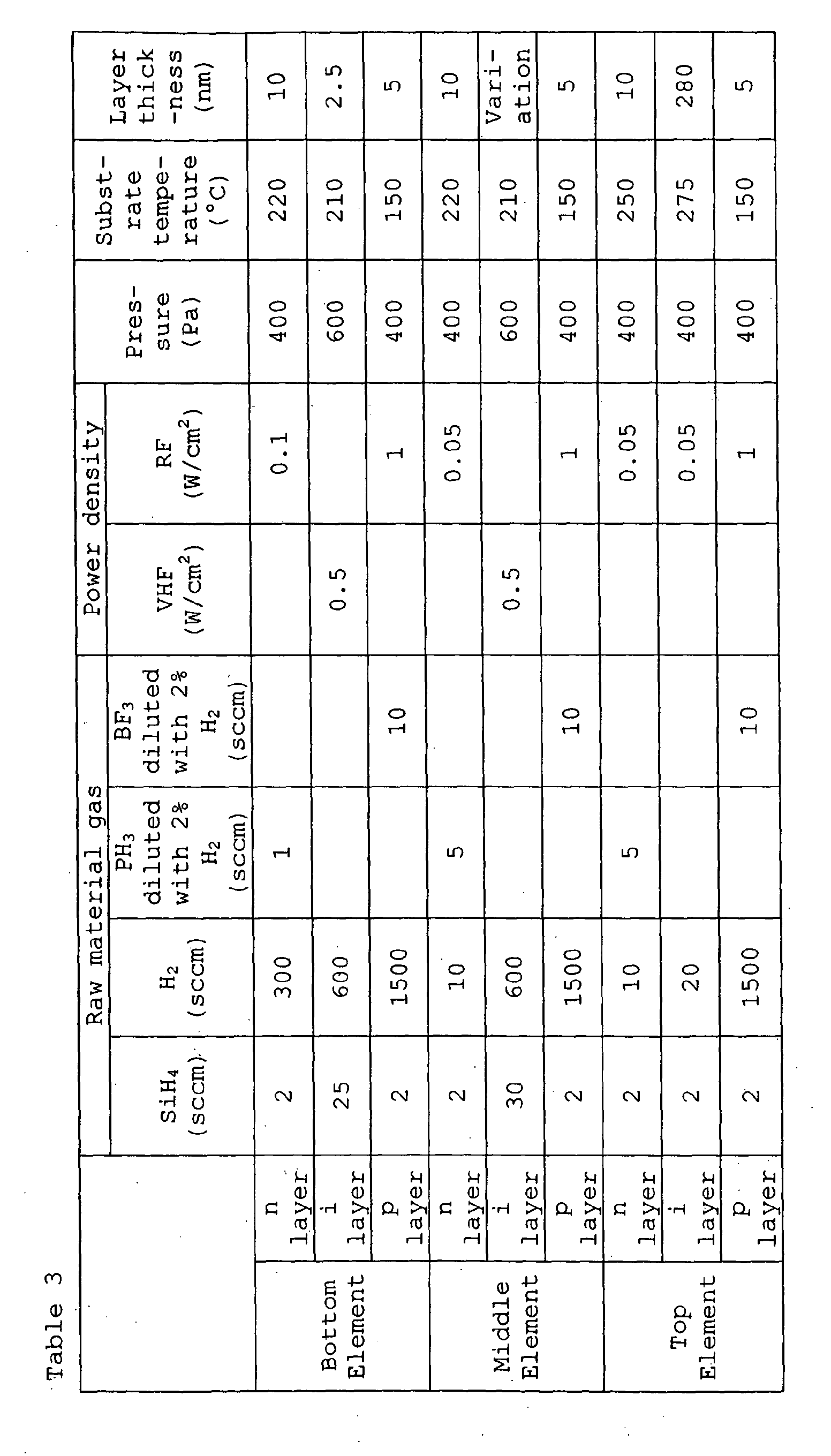
In Table 4, there are shown a value of Voc when
each of the middle element and the bottom element at
that time was manufactured in the form of a single
element, the results of measuring a layer thickness
of the i-type semiconductor layer by utilizing both
the cross section SEM observation method and the
capacitance measurement method, Voc/t, a short-circuit
photoelectric current density of each of the
elements, an initial photoelectric conversion
efficiency, and a photoelectric conversion efficiency
after application of light (1SUN, at 50°C for 1,000
hours). The short-circuit photoelectric current
densities of the top elements were 10.5 mA in both
Example 1 and Comparative Example 1.
From Table 4, it is understood that though the
initial photoelectric conversion efficiency of
Example 1 is equal to that of Comparative Example 1,
the photoelectric conversion efficiency after
degradation is enhanced in a sample of Example 1. In
Example 1, the middle control is provided and Voc/t
of the middle element is large, while in Comparative
Example 1, the bottom control is provided and Voc/t
of the middle element is large. Consequently, it is
confirmed that Voc/t of the control element as the
constitution of the present invention is made large
to greatly enhance the photoelectric conversion
efficiency after degradation.
In addition, a layer thickness measured by
utilizing the cross section SEM observation method
and a layer thickness measured by utilizing the
capacitance measurement method show the same value.
Hence, the diffusion of the doping elements or the
like into the i-type semiconductor layer is at an
ignorable level, and this value of the layer
thickness is adapted for calculation of Voc/t as it
is.
In this example, a layer thickness and film
formation conditions of the reflection enhancing film
were adjusted, whereby the texture degree of a
surface of the reflection enhancing film was greatly
increased as compared with the reflection enhancing
film used in Example 1. As a result, the number of
photons absorbed in the bottom element can be
increased to decrease a layer thickness of the i
layer of the bottom element. Then, in Example 2, the
semiconductor layers were formed under the conditions
shown in Table 3 except that the i layer of the
bottom element was thinned to 20 µm. Similarly to
Example 1, the i-type semiconductor layer of the top
element was made of amorphous silicon, and each of
the i-type semiconductor layers of the middle element
and the bottom element was made of microcrystalline
silicon. In Example 2, there was manufactured the
photovoltaic device such that a layer thickness of
the i layer of the middle element was set to 2.5 µm,
whereby the triple device is made the bottom control
element, and Voc/t of the bottom element was larger
than that of the middle element. In addition, in
Comparative Example 2, there was manufactured the
photovoltaic device such that though a layer
thickness of the middle element was decreased to 2.2
µm to thereby make a triple element a middle control
element, a value of Voc/t of the bottom element was
still larger than that of the middle element.
In Table 5, there are shown a value of Voc when
each of the middle element and the bottom element at
that time was manufactured in the form of a single
element, the results of measuring a layer thickness
of the i-type semiconductor layer by utilizing both
the cross section SEM observation method and the
capacitance measurement method, Voc/t, a short-circuit
photoelectric current density of each of the
elements, an initial photoelectric conversion
efficiency, and a photoelectric conversion efficiency
after application of light (1SUN, at 50°C for 1,000
hours). The short-circuit photoelectric current
densities of the top elements were 10.5 mA/cm2 in
both Example 2 and Comparative Example 2.
From Table 5, it is understood that though the
initial photoelectric conversion efficiency of
Example 2 is equal to that of Comparative Example 2,
the photoelectric conversion efficiency after
degradation is enhanced in a sample of Example 2. In
Example 2, the bottom control is provided and Voc/t
of the bottom element is large, while in Comparative
Example 2, the middle control is provided and Voc/t
of the bottom element is large. Consequently, in
this example as well, it is confirmed that Voc/t of
the control element as the constitution of the
present invention is made large to greatly enhance
the photoelectric conversion efficiency after
degradation.
In addition, a layer thickness measured by
utilizing the cross section SEM observation method
and a layer thickness measured by utilizing the
capacitance measurement method show the same value.
Hence, the diffusion of the doping elements or the
like into the i-type semiconductor layer is at an
ignorable level, and this value of the layer
thickness is adapted for calculation of Voc/t as it
is.
In Example 3, the semiconductor layers were
formed under the same conditions as those of Example
1 shown in Table 3 except that as the conditions of
formation of the n-type semiconductor layer of the
bottom element, a flow rate of PH3 as an n-type
doping gas was made 20 times as high as that in
Example 1 in order to form the n-type semiconductor
layer of the bottom element. While enhancement of
Voc was obtained by increasing the flow rate of PH3,
the short-circuit photoelectric current density of
the bottom element was decreased to provide a bottom
control element, and the same photoelectric
conversion efficiency was obtained. This is
conceived to be because the diffusion of P into the
i-type semiconductor layer exerts an influence on the
results. When the measurement was actually carried
out by utilizing SIMS, it became clear that the
concentration of P in the i-type semiconductor layer
of the bottom element was higher than that of P in
the i-type semiconductor layer of the bottom element
of Example 1 by a half digit on the average. In
addition, similarly to Example 1 and Example 2, the
concentration of P in the i layer of the middle
element in Example 3 and Comparative Examples 3-1 and
3-2 was at an ignorable level. Hence, the i-type
semiconductor layer of the top element was made of
amorphous silicon, and the i-type semiconductor layer
of each of the middle element and the bottom element
was made of microcrystalline silicon. In Comparative
Example 3-1, there was manufactured the photovoltaic
device such that the formation time of the i layer of
the bottom element was increased by 20% to increase
the short-circuit photoelectric current of the bottom
element to change the control over to the middle
control. On the other hand, in Comparative Example
3-2, there was manufactured the photovoltaic device
such that the formation time of the i layer of the
middle element was decreased by 10% as compared with
Example 3 to change the control over to the middle
control.
In Table 6, there are shown a value of Voc when
each of the middle element and the bottom element at
that time was manufactured in the form of a single
element, the results of measuring a layer thickness
of the i-type semiconductor layer by utilizing both
the cross section SEM observation method and the
capacitance measurement method, Voc/t, a short-circuit
photoelectric current density of each of the
elements, an initial photoelectric conversion
efficiency, and a photoelectric conversion efficiency
after application of light (1SUN, at 50°C for 1,000
hours). The short-circuit photoelectric current
densities of all the top elements were 10.5 mA/cm2.
From Table 6, it is understood that though the
initial photoelectric conversion efficiency of
Example 3 is equal to that of Comparative Example 3-1
or Comparative Example 3-2, the photoelectric
conversion efficiency after degradation is enhanced
in a sample of Example 3. In Example 3, the bottom
control is provided and Voc/t of the bottom element
is large, while in Comparative Example 3-1 and
Comparative Example 3-2, the middle control is
provided and Voc/t of the bottom element is large.
Consequently, in this example as well, it is
confirmed that Voc/t of the control element as the
constitution of the present invention is made large
to greatly enhance the photoelectric conversion
efficiency after degradation.
In addition, in Example 3, Comparative Example
3-1, and Comparative Example 3-2, it was made clear
that a layer thickness measured with the capacitance
measurement method was smaller than that measured
with the cross section SEM observation method due to
the diffusion of P into the i layer of the bottom
element. Then, a layer thickness measured with the
capacitance measurement method was adopted for
calculation of Voc/t.
In Example 4, there was manufactured a triple
element which was identical to that of Example 1
except that a layer thickness of the i layer of the
top element was decreased in Example 1 to reduce the
short-circuit photoelectric current density of the
top element to 9.8 mA/cm2. Under this condition,
Example 4 was compared with Example 1. Table 7 shows
a value of Voc, the results of measuring a layer
thickness of the i-type semiconductor layer by
utilizing both the cross section SEM observation
method and the capacitance measurement method, Voc/t,
a density of a short-circuit photoelectric current of
each of the elements, an initial photoelectric
conversion efficiency, and a photoelectric conversion
efficiency after application of light (1SUN, at 50°C
for 1,000 hours) when each of the top element, the
middle element, and the bottom element at that time
was manufactured in the form of a single element.
From Table 7, it is understood that though the
initial photoelectric current efficiency in Example 4
is equal to that in Example 1, the photoelectric
current efficiency after degradation in Example 4 is
slightly reduced as compared with that in Example 1.
It is conceived that this is because since the short-circuit
photoelectric current density of the top
element having the i layer made of amorphous silicon
is lower than that of the bottom element having the i
layer made of microcrystalline silicon, the light
degradation of the top element becomes remarkable.
As a result, it is confirmed that the short-circuit
photoelectric current density of the pin element
having the i-type semiconductor layer made of
amorphous silicon is made larger than that of the pin
element having the i-type semiconductor layer made of
microcrystalline silicon to thereby allow the
photovoltaic device having a higher efficiency to be
formed.
As set forth hereinabove, according to the
present invention, in the stacked photovoltaic device
having a plurality of i-type semiconductor layers
each made of microcrystalline silicon, it is possible
to show the excellent effects such as the
photovoltaic conversion efficiency is high, and the
photoelectric conversion efficiency after application
of light for a long period of time can be maintained
at a high level.
Provided is a stacked photovoltaic device
characterized in that: a first i-type semiconductor
layer comprises amorphous silicon hydride, and second
and subsequent i-type semiconductor layers comprise
amorphous silicon hydride or microcrystalline silicon,
the i-type semiconductor layers being stacked in
order from a light incidence side; and when an open
circuit voltage is assigned Voc in the case where a
pin photoelectric single element is manufactured
using a pin element having the i-type semiconductor
layer made of microcrystalline silicon of pin
elements having the second and subsequent i-type
semiconductor layers, respectively, and a layer
thickness of the i-type semiconductor layer concerned
is assigned t, a short-circuit photoelectric current
density of the stacked photovoltaic device is
controlled by the pin element including the i-type
semiconductor layer having the largest value of Voc/t.