EP1420442A2 - Process for self-aligned manufacture of integrated electronic devices - Google Patents
Process for self-aligned manufacture of integrated electronic devices Download PDFInfo
- Publication number
- EP1420442A2 EP1420442A2 EP03104191A EP03104191A EP1420442A2 EP 1420442 A2 EP1420442 A2 EP 1420442A2 EP 03104191 A EP03104191 A EP 03104191A EP 03104191 A EP03104191 A EP 03104191A EP 1420442 A2 EP1420442 A2 EP 1420442A2
- Authority
- EP
- European Patent Office
- Prior art keywords
- recesses
- process according
- insulation structures
- forming
- conductive regions
- Prior art date
- Legal status (The legal status is an assumption and is not a legal conclusion. Google has not performed a legal analysis and makes no representation as to the accuracy of the status listed.)
- Withdrawn
Links
Images


Classifications
-
- H—ELECTRICITY
- H10—SEMICONDUCTOR DEVICES; ELECTRIC SOLID-STATE DEVICES NOT OTHERWISE PROVIDED FOR
- H10B—ELECTRONIC MEMORY DEVICES
- H10B41/00—Electrically erasable-and-programmable ROM [EEPROM] devices comprising floating gates
- H10B41/40—Electrically erasable-and-programmable ROM [EEPROM] devices comprising floating gates characterised by the peripheral circuit region
-
- H—ELECTRICITY
- H10—SEMICONDUCTOR DEVICES; ELECTRIC SOLID-STATE DEVICES NOT OTHERWISE PROVIDED FOR
- H10B—ELECTRONIC MEMORY DEVICES
- H10B41/00—Electrically erasable-and-programmable ROM [EEPROM] devices comprising floating gates
- H10B41/40—Electrically erasable-and-programmable ROM [EEPROM] devices comprising floating gates characterised by the peripheral circuit region
- H10B41/42—Simultaneous manufacture of periphery and memory cells
-
- H—ELECTRICITY
- H10—SEMICONDUCTOR DEVICES; ELECTRIC SOLID-STATE DEVICES NOT OTHERWISE PROVIDED FOR
- H10D—INORGANIC ELECTRIC SEMICONDUCTOR DEVICES
- H10D84/00—Integrated devices formed in or on semiconductor substrates that comprise only semiconducting layers, e.g. on Si wafers or on GaAs-on-Si wafers
- H10D84/01—Manufacture or treatment
- H10D84/0123—Integrating together multiple components covered by H10D12/00 or H10D30/00, e.g. integrating multiple IGBTs
- H10D84/0126—Integrating together multiple components covered by H10D12/00 or H10D30/00, e.g. integrating multiple IGBTs the components including insulated gates, e.g. IGFETs
- H10D84/0151—Manufacturing their isolation regions
-
- H—ELECTRICITY
- H10—SEMICONDUCTOR DEVICES; ELECTRIC SOLID-STATE DEVICES NOT OTHERWISE PROVIDED FOR
- H10D—INORGANIC ELECTRIC SEMICONDUCTOR DEVICES
- H10D84/00—Integrated devices formed in or on semiconductor substrates that comprise only semiconducting layers, e.g. on Si wafers or on GaAs-on-Si wafers
- H10D84/01—Manufacture or treatment
- H10D84/02—Manufacture or treatment characterised by using material-based technologies
- H10D84/03—Manufacture or treatment characterised by using material-based technologies using Group IV technology, e.g. silicon technology or silicon-carbide [SiC] technology
- H10D84/038—Manufacture or treatment characterised by using material-based technologies using Group IV technology, e.g. silicon technology or silicon-carbide [SiC] technology using silicon technology, e.g. SiGe
-
- H—ELECTRICITY
- H10—SEMICONDUCTOR DEVICES; ELECTRIC SOLID-STATE DEVICES NOT OTHERWISE PROVIDED FOR
- H10D—INORGANIC ELECTRIC SEMICONDUCTOR DEVICES
- H10D84/00—Integrated devices formed in or on semiconductor substrates that comprise only semiconducting layers, e.g. on Si wafers or on GaAs-on-Si wafers
- H10D84/80—Integrated devices formed in or on semiconductor substrates that comprise only semiconducting layers, e.g. on Si wafers or on GaAs-on-Si wafers characterised by the integration of at least one component covered by groups H10D12/00 or H10D30/00, e.g. integration of IGFETs
- H10D84/811—Combinations of field-effect devices and one or more diodes, capacitors or resistors
-
- H—ELECTRICITY
- H10—SEMICONDUCTOR DEVICES; ELECTRIC SOLID-STATE DEVICES NOT OTHERWISE PROVIDED FOR
- H10W—GENERIC PACKAGES, INTERCONNECTIONS, CONNECTORS OR OTHER CONSTRUCTIONAL DETAILS OF DEVICES COVERED BY CLASS H10
- H10W10/00—Isolation regions in semiconductor bodies between components of integrated devices
- H10W10/01—Manufacture or treatment
- H10W10/011—Manufacture or treatment of isolation regions comprising dielectric materials
- H10W10/014—Manufacture or treatment of isolation regions comprising dielectric materials using trench refilling with dielectric materials, e.g. shallow trench isolations
- H10W10/0143—Manufacture or treatment of isolation regions comprising dielectric materials using trench refilling with dielectric materials, e.g. shallow trench isolations comprising concurrently refilling multiple trenches having different shapes or dimensions
-
- H—ELECTRICITY
- H10—SEMICONDUCTOR DEVICES; ELECTRIC SOLID-STATE DEVICES NOT OTHERWISE PROVIDED FOR
- H10W—GENERIC PACKAGES, INTERCONNECTIONS, CONNECTORS OR OTHER CONSTRUCTIONAL DETAILS OF DEVICES COVERED BY CLASS H10
- H10W10/00—Isolation regions in semiconductor bodies between components of integrated devices
- H10W10/01—Manufacture or treatment
- H10W10/011—Manufacture or treatment of isolation regions comprising dielectric materials
- H10W10/014—Manufacture or treatment of isolation regions comprising dielectric materials using trench refilling with dielectric materials, e.g. shallow trench isolations
- H10W10/0145—Manufacture or treatment of isolation regions comprising dielectric materials using trench refilling with dielectric materials, e.g. shallow trench isolations of trenches having shapes other than rectangular or V-shape
-
- H—ELECTRICITY
- H10—SEMICONDUCTOR DEVICES; ELECTRIC SOLID-STATE DEVICES NOT OTHERWISE PROVIDED FOR
- H10W—GENERIC PACKAGES, INTERCONNECTIONS, CONNECTORS OR OTHER CONSTRUCTIONAL DETAILS OF DEVICES COVERED BY CLASS H10
- H10W10/00—Isolation regions in semiconductor bodies between components of integrated devices
- H10W10/10—Isolation regions comprising dielectric materials
- H10W10/17—Isolation regions comprising dielectric materials formed using trench refilling with dielectric materials, e.g. shallow trench isolations
Definitions
- the present invention relates to a process for self-aligned manufacture of integrated electronic devices.
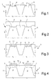
- FIG. 1 showing a semiconductor wafer 1 having a substrate 10, for example of monocrystalline silicon.
- the wafer 1 comprises conductive active areas 2, insulated by shallow-trench-insulation (STI) structures 3, or else, alternatively, by insulation structures formed through local oxidation of silicon (LOCOS).
- the insulation structures 3 comprise trenches of a preset depth, filled with silicon dioxide. In either case, the insulation structures 3 project from the surface 4 of the wafer 1, adjacent to the active areas 2; in this way, the insulation structures 3 define recesses 5 exactly on top of the active areas 2.
- Channel regions of memory cells are made inside the active areas 2 by implanting and diffusing dopant species and using thermal oxidation; then a thermal oxidation provides a gate oxide layer 7, of the thickness of a few nanometers. Subsequently, a conductive polysilicon layer 8 is deposited, as illustrated in Figure 2.
- the conductive layer 8 fills the recesses 5 and has a thickness such as to cover completely the projecting portions of the insulation structures 3.
- the process further comprises forming an insulating layer 12, which coats the floating gates 11 of the polysilicon layer 8, and depositing a further polysilicon layer, which is in turn defined for forming control gates 13 of the memory cells.
- the floating terminal is shaped so as to extend in part also outside of the active areas and is consequently better coupled to the control gate: these cells may consequently be driven more rapidly and/or with lower voltages.
- the aim of the present invention is to provide a self-aligned process for manufacturing integrated electronic devices which is free from the drawbacks described above.
- non-volatile memories in particular of EEPROM or flash type; this is not, however, to be considered limiting, in so far as the process may be used also in electronic devices of another type.
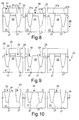
- a semiconductor wafer 20 preferably of silicon, has a substrate 21, for example of P type.
- a hard mask 22 is formed on the wafer 20; the hard mask 22 comprises a pad oxide layer 22a and a silicon nitride layer 22b and has openings 23.
- the substrate 21 of the wafer 20 is etched, and trenches 24 are opened, which delimit memory active areas 25 and circuitry active areas 26, where memory cells and, respectively, read/write circuits and control circuits ( Figure 6) will subsequently be formed.
- the trenches 24 are filled with dielectric material, here silicon dioxide.
- the wafer 20 is then planarized with a first chemical-mechanical-polishing (CMP) treatment; in particular, the CMP treatment is interrupted when the hard mask 22 has been reached, as illustrated in Figure 7.
- CMP chemical-mechanical-polishing
- the active array areas 25 and circuitry-active areas 26 are delimited laterally by trench insulation structures 27, which extend in part inside the substrate 21 and have projecting portions 27a projecting at the top from the substrate 21 and aligned with the hard mask 22.
- a resist mask 28 is formed on top of the wafer 20 and has first and second openings 30, 31 (see Figure 8).
- the first openings 30 are formed on top of some of the memory active areas 25, where high-performance cells are to be formed. More precisely, the first openings 30 expose portions of the hard mask 22 that overlie these active memory areas 25 and, furthermore, laterally expose the projecting portions 27a of the insulation structures 27 adjacent to them.
- the remaining memory active areas 25, designed to accommodate standard cells, are covered by the resist mask 28.
- first and second recesses 32, 33 are dug inside the insulation structures 27, which delimit the memory active areas 25 and, respectively, the circuitry active areas 26.
- first recesses 32 are delimited at the bottom and on one side by the respective insulation structures 27 and, on the opposite side, by portions of the hard mask 22, which coat memory active areas 25.
- the second recesses 33 are, instead, dug completely inside the insulation structures 27, defining the circuitry active areas 26.
- the second recesses 33 are opened and accessible at the top and are delimited laterally and at the bottom by the respective insulation structures 27.
- the resist mask 28 and the hard mask 22 are removed, as illustrated in Figure 10.
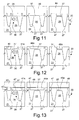
- the first recesses 32 are connected to one another and form, in pairs, cavities 34 above the respective memory active areas 25; furthermore, third recesses 35 are defined on top of the memory active areas 25 intended to accommodate standard memory cells, and are delimited laterally by pairs of insulation structures 27.
- ion-implantation and diffusion are then performed for forming channel regions of memory cells (not illustrated herein for convenience) in the memory active areas 25; simultaneously, electronic components are provided in the circuitry-active areas 26 and form read/write and control circuits 36, here indicated only schematically.
- a gate oxide layer 37 with a thickness of a few nanometers is grown thermally, and coats both the memory active areas 25 and the circuitry active areas 26 ( Figure 11).
- a first polysilicon layer 39 is then deposited on the wafer 20, coats the entire wafer 20 and fills the second and third recesses 33, 35 and the cavities 34.
- the wafer 20 is then planarized with a second CMP treatment, which is stopped when the insulation structures 27 are again exposed, as illustrated in Figure 12.
- the first polysilicon layer 39 is removed completely, except for residual portions inside the second recesses 33, the cavities 34 and the third recesses 35, which form, in the first case, resistors 40 and first plates 41a of capacitors, and in the other cases, floating gates 44a, 45a of high-performance memory cells and standard memory cells, respectively.
- just one deposition of polysilicon, followed by a planarization step enables conductive regions to be formed which extend entirely (resistors 40 and first plates 41a) or partially (floating gates 44a) on top of insulation structures 27.
- the steps described above are moreover self-aligned, in so far as they are formed by exploiting the surface conformation of the wafer 20.
- a dielectric layer 47 and a second polysilicon layer 48 are deposited ( Figure 13) and selectively etched for forming capacitors 41, high-performance cells 44, and standard cells 45.
- Figure 14 starting from the second polysilicon layer 48, second plates 41b are formed on top of the first plates 41a, and control gates 44b, 45b are formed on top of the floating gates 44a, 45a of high-performance cells 44 and standard cells 45, respectively.
- the second plates 41b and the control gates 44b, 45b are insulated from the underlying conductive regions (first plates 41a, floating gates 44a, 45a) by respective residual portions 47' of the dielectric layer 47.
- the floating gates 44a and control gates 44b of the high-performance cells have a greater capacitive coupling than those of the standard cells, since they have a larger surface. They extend, in fact, beyond the respective active areas 25 and occupy the first recesses 32 of the adjacent insulation structures 27.
- the process then comprises depositing a protective dielectric layer 50, for example of silicon dioxide, and opening contacts 51 through the protective layer 50, figure 15.
- a protective dielectric layer 50 for example of silicon dioxide
- opening contacts 51 through the protective layer 50 figure 15.
- the wafer 20 is divided into individual dice 52, as illustrated in Figure 16; each die 52 comprises a respective electronic device, which, in the described embodiment, is a non-volatile memory.
- the process according to the invention is clearly advantageous, because, through the addition of just one masked etch of the insulation structures 27, it enables both passive components presenting excellent insulation from the substrate 21 and memory cells with differentiated characteristics and performance to be formed on the same wafer 20.
- the passive components may operate with high voltages, without any risk of breakdown of the insulating dielectric and, furthermore, with a substantially negligible capacitive coupling to the substrate 21.
- These components are consequently suited for being used in read/write circuits, for example for forming charge pumps.
- the process enables cells with high capacitive coupling between the control gate and the floating gate to be formed, in addition to the standard cells.
- the high capacitive coupling is useful because the memory cells formed in this way may be driven with low voltages and hence have optimized performance.
- Memory cells of this type are particularly advantageous in the case of so-called "embedded" memories, which also integrate high-complexity logic circuits, such as, for example, microcontrollers or digital signal processors (DSPs).
- DSPs digital signal processors
- the definition of the resist mask 28 for etching the insulation structures 27 is not critical and does not present problems of alignment with the active areas.
- the process is self-aligned and consequently enables standard cells of extremely contained dimensions to be formed.
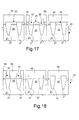
- Figures 17 and 18, where parts equal to those already illustrated are designated by the same reference numbers, show a different embodiment of the process according to the invention.
- a first resist mask 55 is deposited and defined, to expose only a part of insulation structures 27 delimiting memory active areas 25; the insulation structures which delimit the circuitry-active areas 26 are instead protected ( Figure 17).
- the first recesses 32 are then formed.
- a second resist mask 56 is formed on top of the wafer 20. Now, all the memory active areas 25 and the respective insulation structures 27 are protected, while central portions of the insulation structures, which delimit the circuitry-active areas 26, are left exposed.
- the wafer 20 is again etched in a controlled way, and the second recesses 33 are dug.
- the second resist mask 56 is then removed, and the procedure ends with deposition of the first polysilicon layer 28, second CMP treatment, and formation of passive components and memory cells, as already described with reference to Figures 13 to 16.
- the process enables recesses having a differentiated depth to be formed.
- the first recesses 32 in fact, must accommodate a polysilicon layer of thickness sufficient for withstanding the CMP treatment without undergoing damage, but at the same time must never have a depth such as to uncover the memory active areas 25. According to the design specifications of the individual storage device, instead, it could be convenient to form second deeper recesses 33.
- first and second recesses 32, 33 may be performed either before or after removal of the hard mask 22.
- the first recesses 32 could be dug also only in the insulation structures 27 which delimit one side of the memory-active areas 25, and not in those which delimit the other sides; in practice, for each memory-active area, only a first recess 32 is defined.
- the storage devices obtained according to the present process need not necessarily comprise both passive components formed on top of the insulation structures and high-performance memory cells; instead, the process may also be exploited for forming only resistors, only capacitors, or else only high-performance memory cells.
- the process may be used also for forming devices other than non-volatile memories, such as for example volatile memories.
Landscapes
- Engineering & Computer Science (AREA)
- Manufacturing & Machinery (AREA)
- Semiconductor Memories (AREA)
- Non-Volatile Memory (AREA)
- Electrodes Of Semiconductors (AREA)
- Internal Circuitry In Semiconductor Integrated Circuit Devices (AREA)
Abstract
Description
- Figures 1 to 16 are cross-sectional views through a semiconductor wafer in successive fabrication steps of a process according to a first embodiment of the present invention; and
- Figures 17 and 18 are cross-sectional views through a semiconductor wafer in successive fabrication steps of a process according to a different embodiment of the present invention.
Claims (25)
- A process for self-aligned manufacturing integrated electronic devices, comprising the steps of:characterized by, prior to forming said first conductive layer (28), forming recesses in said insulation structures (27).forming, in a semiconductor wafer (20) having a substrate (21), insulation structures (27) delimiting active areas (25, 26) and projecting from said substrate (21);forming a first conductive layer (39) coating said insulation structures (27) and said active areas (25, 26); andpartially removing said first conductive layer (28);
- The process according to claim 1, characterized in that said step of forming said first conductive layer (39) comprises depositing said first conductive layer and filling said insulation structures (27).
- The process according to claim 1 or 2, characterized in that said step of forming recesses comprises removing side portions (27a) of said insulation structures (27) so as to form first recesses (32).
- The process according to claim 3, characterized in that said first recesses are defined on top and at the side of respective said active areas (25).
- The process according to claim 3 or 4, characterized in that said step of partial removing comprises forming first conductive regions (44a), which extend inside at least one of said first recesses (32) and on top of a respective said active area (25).
- The process according to claim 5, characterized in that said first conductive regions (44a) are floating gates of respective first memory cells (44).
- The process according to any one of the preceding claims, characterized in that said step of forming recesses comprises removing central portions (27b) of said insulation structures (27) so as to form second recesses (33).
- The process according to claim 7, characterized in that said second recesses (33) are delimited laterally and at the bottom by respective said insulation structures (27).
- The process according to claim 8 or 9, characterized in that said step of partial removing comprises forming second conductive regions (40, 41a), accommodated inside respective said second recesses (33).
- The process according to claim 9, characterized in that said second conductive regions (40) comprise resistors.
- The process according to claim 9 or 10, characterized in that said second conductive regions (41a) comprise first plates of respective capacitors (41).
- The process according to any one of the preceding claims, characterized in that said step of forming recesses comprises performing at least one first masked etch of said insulation structures (27).
- The process according to claim 12, characterized in that said step of digging comprises performing a second masked etch of said insulation structures (27).
- The process according to any one of the preceding claims, characterized in that said step of partially removing comprises planarizing said wafer (20).
- The process according to any one of the preceding claims, characterized in that said step of partially removing is followed by the steps of:forming a dielectric layer (47) on top of said wafer (20);forming a second conductive layer (48) on top of said dielectric layer (47); andselectively removing said dielectric layer (47) and said second conductive layer (48).
- The process according to claim 15, characterized in that said step of selectively removing comprises forming third conductive regions (41b, 44b).
- The process according to claims 6 and 16, characterized in that said third conductive regions (44b) comprise control gates of said memory cells (44).
- The process according to claims 11 and 16, characterized in that said third conductive regions (41b) comprise second plates of said capacitors (41).
- An integrated electronic device comprising:a semiconductor body (20) having a substrate (21); anda plurality of insulation structures (27) delimiting active areas (25, 26) and having respective portions (27a) projecting from said substrate (21); characterized in that said insulation structures (27) have respective recesses (32, 33), which accommodate at least partially conductive regions (40, 41a, 44a).
- The device according to claim 19, characterized in that said recesses (32) are defined laterally with respect to respective projecting portions (27a) of said insulation structures (27).
- The device according to claim 19 or 20, characterized in that said conductive regions (44a) comprise terminals of memory cells (44) arranged on top of respective said active areas (25) and extending laterally inside at least one of said recesses (32).
- The device according to claim 19, characterized in that said recesses (33) are defined centrally with respect to respective said projecting portions (27a) of said insulation structures (27).
- The device according to claim 22, characterized in that said conductive regions (40, 41a) are entirely accommodated inside respective said recesses (33).
- The device according to claim 22 or claim 23, characterized in that said conductive regions (40) comprise resistors.
- The device according to any one of claims 22 to 24, characterized in that said conductive regions (41a) comprise first plates of capacitors (41).
Applications Claiming Priority (2)
| Application Number | Priority Date | Filing Date | Title |
|---|---|---|---|
| IT000997A ITTO20020997A1 (en) | 2002-11-15 | 2002-11-15 | SELF-ALIGNED PROCEDURE FOR THE MANUFACTURE OF |
| ITTO20020997 | 2002-11-15 |
Publications (2)
| Publication Number | Publication Date |
|---|---|
| EP1420442A2 true EP1420442A2 (en) | 2004-05-19 |
| EP1420442A3 EP1420442A3 (en) | 2004-12-22 |
Family
ID=32170757
Family Applications (1)
| Application Number | Title | Priority Date | Filing Date |
|---|---|---|---|
| EP03104191A Withdrawn EP1420442A3 (en) | 2002-11-15 | 2003-11-13 | Process for self-aligned manufacture of integrated electronic devices |
Country Status (3)
| Country | Link |
|---|---|
| US (2) | US7468535B2 (en) |
| EP (1) | EP1420442A3 (en) |
| IT (1) | ITTO20020997A1 (en) |
Families Citing this family (5)
| Publication number | Priority date | Publication date | Assignee | Title |
|---|---|---|---|---|
| US7306552B2 (en) * | 2004-12-03 | 2007-12-11 | Samsung Electronics Co., Ltd. | Semiconductor device having load resistor and method of fabricating the same |
| JP2012043856A (en) * | 2010-08-16 | 2012-03-01 | Toshiba Corp | Semiconductor device and method for manufacturing the same |
| KR101770585B1 (en) * | 2010-09-03 | 2017-08-24 | 삼성전자주식회사 | Resistor array and Semiconductor memory device including the same |
| US10622073B2 (en) * | 2018-05-11 | 2020-04-14 | Texas Instruments Incorporated | Integrated circuit including vertical capacitors |
| TWI852393B (en) * | 2023-03-10 | 2024-08-11 | 華邦電子股份有限公司 | Semiconductor device and method of forming the same |
Citations (10)
| Publication number | Priority date | Publication date | Assignee | Title |
|---|---|---|---|---|
| US5449636A (en) | 1993-07-27 | 1995-09-12 | Hyundai Electronics Industries Co., Ltd. | Method for the fabrication of DRAM cell having a trench in the field oxide |
| US6090661A (en) | 1998-03-19 | 2000-07-18 | Lsi Logic Corporation | Formation of novel DRAM cell capacitors by integration of capacitors with isolation trench sidewalls |
| US20010005616A1 (en) | 1999-12-23 | 2001-06-28 | Kim Jae Kap | Method for fabricating semiconductor device |
| US20010052610A1 (en) | 1998-08-14 | 2001-12-20 | Wingyu Leung | Reduced topography DRAM cell fabricated using a modified logic process and method for operating same |
| US20020019114A1 (en) | 2000-03-01 | 2002-02-14 | Trivedi Jigish D. | Methods of forming integrated circuitry. |
| US6362071B1 (en) | 2000-04-05 | 2002-03-26 | Motorola, Inc. | Method for forming a semiconductor device with an opening in a dielectric layer |
| US6373083B1 (en) | 1999-04-20 | 2002-04-16 | Hyundai Electronics Industries Co., Ltd. | Capacitor for semiconductor device and fabrication method thereof |
| US20020072197A1 (en) | 2000-07-25 | 2002-06-13 | Samsung Electronics Co., Ltd. | Method for self-aligned shallow trench isolation and method of manufacturing non-volatile memory device using the same |
| US6420749B1 (en) | 2000-06-23 | 2002-07-16 | International Business Machines Corporation | Trench field shield in trench isolation |
| US6448606B1 (en) | 2000-02-24 | 2002-09-10 | Advanced Micro Devices, Inc. | Semiconductor with increased gate coupling coefficient |
Family Cites Families (10)
| Publication number | Priority date | Publication date | Assignee | Title |
|---|---|---|---|---|
| US6403421B1 (en) * | 1998-04-22 | 2002-06-11 | Sony Corporation | Semiconductor nonvolatile memory device and method of producing the same |
| US6420729B2 (en) | 1999-03-16 | 2002-07-16 | Texas Instruments Incorporated | Process to produce ultrathin crystalline silicon nitride on Si (111) for advanced gate dielectrics |
| JP2002064157A (en) * | 2000-06-09 | 2002-02-28 | Toshiba Corp | Semiconductor memory integrated circuit and method of manufacturing the same |
| JP2002043384A (en) * | 2000-07-24 | 2002-02-08 | Mitsubishi Electric Corp | Semiconductor device including TEG for evaluating interlayer insulating film, method of manufacturing the same, and method of evaluating interlayer insulating film |
| JP2003007869A (en) * | 2001-06-26 | 2003-01-10 | Fujitsu Ltd | Semiconductor device and manufacturing method thereof |
| US6737333B2 (en) * | 2001-07-03 | 2004-05-18 | Texas Instruments Incorporated | Semiconductor device isolation structure and method of forming |
| US6696742B2 (en) * | 2001-10-16 | 2004-02-24 | Infineon Technologies Ag | Semiconductor memory device |
| US6682977B2 (en) * | 2002-02-11 | 2004-01-27 | Winbond Electronics Corporation | Method for fabricating a gate structure of a flash memory |
| CN100340001C (en) * | 2002-06-19 | 2007-09-26 | 桑迪士克股份有限公司 | Deep wordline trench to shield cross coupling between adjacent cells for scaled NAND |
| US6974708B2 (en) * | 2004-04-08 | 2005-12-13 | Headway Technologies, Inc. | Oxidation structure/method to fabricate a high-performance magnetic tunneling junction MRAM |
-
2002
- 2002-11-15 IT IT000997A patent/ITTO20020997A1/en unknown
-
2003
- 2003-11-13 EP EP03104191A patent/EP1420442A3/en not_active Withdrawn
- 2003-11-14 US US10/713,538 patent/US7468535B2/en not_active Expired - Lifetime
-
2008
- 2008-01-04 US US12/006,706 patent/US7772084B2/en not_active Expired - Lifetime
Patent Citations (10)
| Publication number | Priority date | Publication date | Assignee | Title |
|---|---|---|---|---|
| US5449636A (en) | 1993-07-27 | 1995-09-12 | Hyundai Electronics Industries Co., Ltd. | Method for the fabrication of DRAM cell having a trench in the field oxide |
| US6090661A (en) | 1998-03-19 | 2000-07-18 | Lsi Logic Corporation | Formation of novel DRAM cell capacitors by integration of capacitors with isolation trench sidewalls |
| US20010052610A1 (en) | 1998-08-14 | 2001-12-20 | Wingyu Leung | Reduced topography DRAM cell fabricated using a modified logic process and method for operating same |
| US6373083B1 (en) | 1999-04-20 | 2002-04-16 | Hyundai Electronics Industries Co., Ltd. | Capacitor for semiconductor device and fabrication method thereof |
| US20010005616A1 (en) | 1999-12-23 | 2001-06-28 | Kim Jae Kap | Method for fabricating semiconductor device |
| US6448606B1 (en) | 2000-02-24 | 2002-09-10 | Advanced Micro Devices, Inc. | Semiconductor with increased gate coupling coefficient |
| US20020019114A1 (en) | 2000-03-01 | 2002-02-14 | Trivedi Jigish D. | Methods of forming integrated circuitry. |
| US6362071B1 (en) | 2000-04-05 | 2002-03-26 | Motorola, Inc. | Method for forming a semiconductor device with an opening in a dielectric layer |
| US6420749B1 (en) | 2000-06-23 | 2002-07-16 | International Business Machines Corporation | Trench field shield in trench isolation |
| US20020072197A1 (en) | 2000-07-25 | 2002-06-13 | Samsung Electronics Co., Ltd. | Method for self-aligned shallow trench isolation and method of manufacturing non-volatile memory device using the same |
Also Published As
| Publication number | Publication date |
|---|---|
| US7772084B2 (en) | 2010-08-10 |
| US20080108200A1 (en) | 2008-05-08 |
| US20040173869A1 (en) | 2004-09-09 |
| EP1420442A3 (en) | 2004-12-22 |
| US7468535B2 (en) | 2008-12-23 |
| ITTO20020997A1 (en) | 2004-05-16 |
Similar Documents
| Publication | Publication Date | Title |
|---|---|---|
| US7709347B2 (en) | Semiconductor device and method of fabricating the same | |
| KR101166268B1 (en) | Semiconductor device having dual-stishallow trench isolation and manufacturing method thereof | |
| US6413821B1 (en) | Method of fabricating semiconductor device including nonvolatile memory and peripheral circuit | |
| US8674431B2 (en) | Non-volatile semiconductor memory device and method of manufacturing the same | |
| US6790729B1 (en) | Method of manufacturing NAND flash memory device | |
| US7262093B2 (en) | Structure of a non-volatile memory cell and method of forming the same | |
| US20070026633A1 (en) | Semiconductor device and related method | |
| US6784039B2 (en) | Method to form self-aligned split gate flash with L-shaped wordline spacers | |
| KR20020086639A (en) | Nonvolatile semiconductor memory device and its manufacturing method | |
| US20030194841A1 (en) | Method for manufacturing semiconductor device | |
| US7772084B2 (en) | Process for self-aligned manufacture of integrated electronic devices | |
| US6709924B1 (en) | Fabrication of shallow trench isolation structures with rounded corner and self-aligned gate | |
| US20070235836A1 (en) | Method of forming a shallow trench isolation structure with reduced leakage current in a semiconductor device | |
| US6501123B2 (en) | High gate coupling non-volatile memory structure | |
| US6992348B2 (en) | Semiconductor memory with vertical charge-trapping memory cells and fabrication | |
| US6048768A (en) | Method of manufacturing flash memory | |
| US20030219944A1 (en) | Method for manufacturing a nonvolatile memory device | |
| US7374999B2 (en) | Semiconductor device | |
| KR100823395B1 (en) | Semiconductor device and manufacturing method thereof | |
| US7094644B2 (en) | Method for manufacturing a semiconductor device | |
| KR100724154B1 (en) | Nonvolatile Memory with High Gate-Coupling Capacitance | |
| US20020187615A1 (en) | Method for forming isolations in memory devices with common source lines | |
| US7351636B2 (en) | Methods of forming split-gate non-volatile memory cells including raised oxide layers on field oxide regions | |
| US6380034B1 (en) | Process for manufacturing memory cells with dimensional control of the floating gate regions | |
| US7038304B2 (en) | Semiconductor memory device and manufacturing method thereof |
Legal Events
| Date | Code | Title | Description |
|---|---|---|---|
| PUAI | Public reference made under article 153(3) epc to a published international application that has entered the european phase |
Free format text: ORIGINAL CODE: 0009012 |
|
| AK | Designated contracting states |
Kind code of ref document: A2 Designated state(s): AT BE BG CH CY CZ DE DK EE ES FI FR GB GR HU IE IT LI LU MC NL PT RO SE SI SK TR |
|
| AX | Request for extension of the european patent |
Extension state: AL LT LV MK |
|
| PUAL | Search report despatched |
Free format text: ORIGINAL CODE: 0009013 |
|
| AK | Designated contracting states |
Kind code of ref document: A3 Designated state(s): AT BE BG CH CY CZ DE DK EE ES FI FR GB GR HU IE IT LI LU MC NL PT RO SE SI SK TR |
|
| AX | Request for extension of the european patent |
Extension state: AL LT LV MK |
|
| RIC1 | Information provided on ipc code assigned before grant |
Ipc: 7H 01L 27/06 B Ipc: 7H 01L 21/8234 B Ipc: 7H 01L 21/8247 B Ipc: 7H 01L 21/763 B Ipc: 7H 01L 21/762 A |
|
| 17P | Request for examination filed |
Effective date: 20050621 |
|
| AKX | Designation fees paid |
Designated state(s): DE FR GB IT |
|
| RAP1 | Party data changed (applicant data changed or rights of an application transferred) |
Owner name: STMICROELECTRONICS SRL |
|
| RAP1 | Party data changed (applicant data changed or rights of an application transferred) |
Owner name: STMICROELECTRONICS SRL |
|
| RAP1 | Party data changed (applicant data changed or rights of an application transferred) |
Owner name: MICRON TECHNOLOGY, INC. |
|
| STAA | Information on the status of an ep patent application or granted ep patent |
Free format text: STATUS: THE APPLICATION IS DEEMED TO BE WITHDRAWN |
|
| 18D | Application deemed to be withdrawn |
Effective date: 20130115 |