EP1420420A2 - Planar transformer arrangement - Google Patents
Planar transformer arrangement Download PDFInfo
- Publication number
- EP1420420A2 EP1420420A2 EP03014708A EP03014708A EP1420420A2 EP 1420420 A2 EP1420420 A2 EP 1420420A2 EP 03014708 A EP03014708 A EP 03014708A EP 03014708 A EP03014708 A EP 03014708A EP 1420420 A2 EP1420420 A2 EP 1420420A2
- Authority
- EP
- European Patent Office
- Prior art keywords
- planar
- winding
- meandering
- primary
- voltage
- Prior art date
- Legal status (The legal status is an assumption and is not a legal conclusion. Google has not performed a legal analysis and makes no representation as to the accuracy of the status listed.)
- Withdrawn
Links
Images


Classifications
-
- H—ELECTRICITY
- H01—ELECTRIC ELEMENTS
- H01F—MAGNETS; INDUCTANCES; TRANSFORMERS; SELECTION OF MATERIALS FOR THEIR MAGNETIC PROPERTIES
- H01F27/00—Details of transformers or inductances, in general
- H01F27/28—Coils; Windings; Conductive connections
- H01F27/32—Insulating of coils, windings, or parts thereof
- H01F27/323—Insulation between winding turns, between winding layers
-
- H—ELECTRICITY
- H01—ELECTRIC ELEMENTS
- H01F—MAGNETS; INDUCTANCES; TRANSFORMERS; SELECTION OF MATERIALS FOR THEIR MAGNETIC PROPERTIES
- H01F17/00—Fixed inductances of the signal type
- H01F17/0006—Printed inductances
- H01F17/0013—Printed inductances with stacked layers
-
- H—ELECTRICITY
- H01—ELECTRIC ELEMENTS
- H01F—MAGNETS; INDUCTANCES; TRANSFORMERS; SELECTION OF MATERIALS FOR THEIR MAGNETIC PROPERTIES
- H01F27/00—Details of transformers or inductances, in general
- H01F27/28—Coils; Windings; Conductive connections
- H01F27/2804—Printed windings
-
- H—ELECTRICITY
- H01—ELECTRIC ELEMENTS
- H01F—MAGNETS; INDUCTANCES; TRANSFORMERS; SELECTION OF MATERIALS FOR THEIR MAGNETIC PROPERTIES
- H01F27/00—Details of transformers or inductances, in general
- H01F27/34—Special means for preventing or reducing unwanted electric or magnetic effects, e.g. no-load losses, reactive currents, harmonics, oscillations, leakage fields
- H01F27/343—Preventing or reducing surge voltages; oscillations
- H01F27/345—Preventing or reducing surge voltages; oscillations using auxiliary conductors
-
- H—ELECTRICITY
- H01—ELECTRIC ELEMENTS
- H01F—MAGNETS; INDUCTANCES; TRANSFORMERS; SELECTION OF MATERIALS FOR THEIR MAGNETIC PROPERTIES
- H01F17/00—Fixed inductances of the signal type
- H01F2017/0093—Common mode choke coil
-
- H—ELECTRICITY
- H01—ELECTRIC ELEMENTS
- H01F—MAGNETS; INDUCTANCES; TRANSFORMERS; SELECTION OF MATERIALS FOR THEIR MAGNETIC PROPERTIES
- H01F19/00—Fixed transformers or mutual inductances of the signal type
- H01F19/04—Transformers or mutual inductances suitable for handling frequencies considerably beyond the audio range
- H01F19/08—Transformers having magnetic bias, e.g. for handling pulses
- H01F2019/085—Transformer for galvanic isolation
-
- H—ELECTRICITY
- H01—ELECTRIC ELEMENTS
- H01F—MAGNETS; INDUCTANCES; TRANSFORMERS; SELECTION OF MATERIALS FOR THEIR MAGNETIC PROPERTIES
- H01F27/00—Details of transformers or inductances, in general
- H01F27/28—Coils; Windings; Conductive connections
- H01F27/2804—Printed windings
- H01F2027/2819—Planar transformers with printed windings, e.g. surrounded by two cores and to be mounted on printed circuit
Definitions
- the present invention relates to a planar transformer arrangement and method for isolating driver circuitry and communication circuitry to eliminate magnetic field interference and parasitic capacitance.
- Transformers are often used in floating gate driver circuits for driving high power/voltage switches, for example, high voltage IGBTs for motor control and other applications.
- a transformer provides isolation between low voltage driver circuitry and high voltage power switch circuitry.
- Such transformers may also be employed to communicate data signals between electrically isolated circuits (e.g., to communicate signals via a transceiver).
- transformers inherently exhibit two kinds of parasitic capacitances: distributed parasitic capacitances between adjacent windings on a transformer; and interwinding parasitic capacitances between primary and secondary windings of the transformer. These parasitic capacitances result from the close proximity between transformer windings.
- the magnetic cor is generally arranged between the primary and secondary windings of the transformer, so that the magnetic field generated by the transformer may be better conducted.
- operation of the transformer may induce the flow of disadvantageous currents within the magnetic core, if the core, for example, contacts the transformer windings. These currents may result in a degradation of the galvanic insulation between primary and secondary windings.
- an externally applied magnetic field may result in disadvantageous common mode magnetic interference within conventional transformers.
- Such a magnetic field may induce the flow of unwanted currents within the primary and/or secondary windings of the transformer.
- These common-mode currents may cause a magnetic flux to form around the conductors of the primary and/or secondary windings, thereby inducing noise within the windings.
- a dielectric layer of the planar medium e.g., the printed circuit board or a dielectric oxide layer of the integrated circuit
- the voltage isolation provided by the planar medium permits the present invention to be used, for example, in circuits that isolate a gate driver from high voltage IGBT power switches, which may operate at high voltages and at high currents.
- the planar transformer arrangement includes a second planar transformer comprising at least one second primary winding provided on one layer (e.g., on one side) of the planar medium, and at least one second secondary winding provided on another layer (e.g., the other side) of the planar medium.
- a differential amplifier arrangement may be used to detect and compensate for common mode electromagnetic interference applied to the two planar transformers (e.g., to compensate for noise caused by an external magnetic field and/or parasitic capacitance between windings).
- the magnetic mode interference is canceled without using a differential amplifier circuit.
- each of the windings of the planar transformer includes two windings connected in anti-series. In this manner, magnetic common mode interference may be automatically canceled without need for external compensating circuitry, such as a differential amplifier circuit.
- two respective metallic shields are provided between the two windings and coupled respectively to primary and secondary ground voltages.
- the shields help prevent interwinding parasitic capacitance from interfering with the planar transformers by operating to magnetically isolate the magnetic flux produced by the interwinding parasitic capacitance.
- Planar transformer arrangement 100 includes a planar transformer 105 having primary and secondary windings 105a, 105b arranged on respective sides of a planar medium (not shown), e.g., a printed circuit board or an integrated circuit, a single mode detect winding 110 on the same side of the planar medium as the secondary winding 105b, a mode interference elimination circuit 115 electrically connected to the secondary winding 105b of the planar transformer 105 and the single mode detect winding 110.
- a planar medium not shown
- a single mode detect winding 110 on the same side of the planar medium as the secondary winding 105b
- a mode interference elimination circuit 115 electrically connected to the secondary winding 105b of the planar transformer 105 and the single mode detect winding 110.
- the exemplary planar transformer arrangement 100 of Figure 1 is operable to communicate an input signal 120 applied to the primary winding 105a of the planar transformer 105 to an output signal 125, while providing voltage isolation between the input signal 120 and the output signal 125.
- an input signal 120 applied to the primary winding 105a of the planar transformer 105 induces a current flow within the primary winding 105a.
- the magnetic flux caused by the increasing current flow induces a voltage signal (S) across the secondary winding 105b of the planar transformer 105, which is then transmitted by the mode interference elimination circuit 115 as output signal 125.
- the mode interference elimination circuit 115 is also configured to prevent common mode magnetic noise interference from corrupting the signal flow between the input and output signals 120, 125.
- Mode interference elimination circuit 115 includes a summation circuit 205 having a high impedance positive inpuc 205a electrically connected to the voltage (S) across the secondary winding 105b, and a high impedance negative input 205b electrically connected to the voltage (R) across the mode detect winding 110.
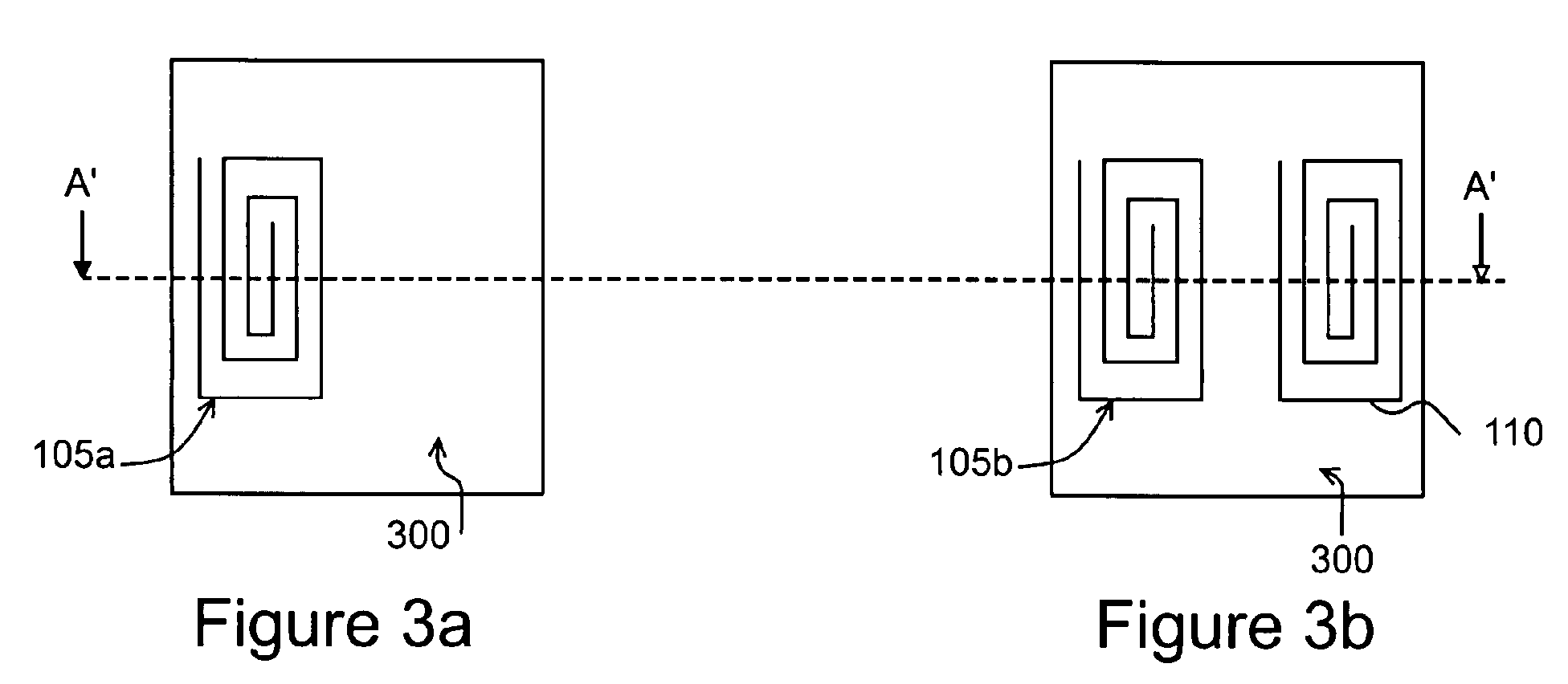
- FIG. 3a through 3c there is seen top, bottom, and cross-sectional views, respectively, of the exemplary planar transformer 105 and exemplary mode detect winding 110 shown in Figure 1.
- the windings 105a, 105b, 110 of the exemplary planar transformer arrangement 100 may be implemented, for example, as meandering traces on a planar medium 300 (e.g., a printed circuit board or an integrated circuit), which forms an open magnetic path between the primary and secondary windings 105a, 105b of the planar transformer 105.
- a planar medium 300 e.g., a printed circuit board or an integrated circuit
- the planar transformer arrangement 500 includes primary circuitry 505a arranged on one side of a planar medium (not shown) and secondary circuitry 505b arranged on the other side of the planar medium (not shown).
- the primary and secondary circuitry 505a, 505b may be arranged on separate silicon dies or, alternatively, may be arranged on the same silicon die. If the primary and secondary circuitry 505a, 505b are arranged on separate dies, magnetic coupling between the circuitry 505a, 505b may be effected using two metal interconnection. layers separated by a dielectric layer.
- Planar transformer arrangement 500 is operable as an isolation transceiver to permit input signals (QR') and (QS') of primary circuitry 505a to be communicated as respective output voltage signals (R'') and (S'') of secondary circuitry 505b, and to permit input signals (QR'') and (QS'') of the secondary circuitry 505b to be communicated as respective output voltage signals (R') and (S') of primary circuitry 505a. In this manner, various signals may be communicated between the primary circuitry 505a and the secondary circuitry 505b, while maintaining electrical isolation.
- primary circuitry 505a includes a primary winding (A) electrically connected to both the negative input terminal of a comparator 530a and the positive input terminal of a comparator 530b via resistor network 520, and a primary winding (B) electrically connected to both the positive input terminal of the comparator 530a and the negative input terminal of the comparator 530b via the resistor network 520.
- the first and second primary windings (A), (B) are also electrically connected in parallel to respective diodes 510b, 515b, resistors 510c, 515c, and capacitors 510d, 515d, all of which terminate at source voltage 501.
- Secondary circuitry 505b includes a secondary winding (C) electrically connected to both the negative input terminal of a comparator 560a and the positive input terminal of a comparator 560b via resistor network 550, and a secondary winding (D) electrically connected to both the positive input terminal of the comparator 560a and the negative input terminal of the comparator 560b via the resistor network 550.
- the first and second secondary windings (C), (D) are also electrically connected in parallel to respective diodes 540b, 545b, resistors 540c, 545c, and capacitors 540d, 545d, all of which terminate at source voltage 502.
- each of the primary and secondary windings (A), (B) , (C) , (D) is implemented as a separate meandering trace on a planar medium 300 (e.g., a printed circuit board or integrated circuit), with primary windings (A), (B) being arranged on one layer (e.g., one side) of planar medium 300 and secondary windings (C), (D) being arranged on another layer (e.g., the other side) of planar medium 300.
- a planar medium 300 e.g., a printed circuit board or integrated circuit
- primary winding (A) is arranged over secondary winding (C) to form a first planar transformer 605a
- primary winding (B) is arranged over secondary winding (D) to form a second planar transformer 605b, as shown in Figure 6c.
- a pulsed input signal for example, signal (QR')
- QR' a pulsed input signal
- a current will be induced within the primary winding (A).
- the magnetic flux caused by the increasing current flow induces a voltage across the secondary winding (C) of the first planar transformer 605a, which causes the comparator 560b of the secondary circuitry 505b to produce a positive output voltage signal (R'').
- the primary windings (A), (B) and the secondary windings (C), (D) are arranged adjacent to one another on respective sides of the planar medium, common mode magnetic interference caused by an externally applied magnetic field will induce an interference voltage across both the secondary windings (C), (D).
- the output stage of the secondary circuitry 505b includes two differential comparators 560a, 560b, the interference voltage caused by the common mode magnetic field is effectively eliminated. Specifically, the output stage of the secondary circuitry 505b provides the interference voltage to both the positive and negative inputs of the output comparator 560b, thereby canceling the disadvantageous effects of the interference voltage on the output voltage signal (R'').
- the magnetic mode interference may be more effectively canceled by arranging the primary windings (A), (B) and the secondary windings (C), (D) adjacent to one another on respective layers of the planar medium.
- the primary windings (A), (B) and the secondary windings (C), (D) may be arranged at a distance from one another, if a particular application of the present invention does not require the compensation of effects caused by common mode magnetic field interference.
- the exemplary planar transformer arrangement 500 may operate as a transceiver between the primary and secondary circuits 505a, 505b.
- the primary windings (A), (B) of planar transformers 605a, 605b and the secondary windings (C), (D) of planar transformers 605a, 605b are provided with respective magnetic cores 405a, 405b (e.g., ferrite) for magnetically coupling the respective windings (A), (B), (C), (D).
- respective magnetic cores 405a, 405b e.g., ferrite
- the two windings (A) and (C) of the first planar transformer 605a are coupled through both magnetic cores 405a, 405b and through the open magnetic circuit (e.g., 25kv/mm) provided by the planar medium 300.
- the two windings (B) and (D) of the second planar transformer 605b are coupled by the same two magnetic cores 405a, 405b and by the open magnetic circuit provided by the planar medium 300.
- each of the primary windings (A), (B) and secondary windings (C), (D) is formed from two sub-windings connected in anti-series.
- primary winding (A) is formed from two sub-windings (A 1 ), (A 2 ) connected in anti-series
- primary winding (B) is formed from two sub-windings (B 1 ), (B 2 ) connected in anti-series
- secondary winding (C) is formed from two sub-windings (C 1 ), (C 2 ) connected in anti-series
- secondary winding (D) is formed from two sub-windings (D 1 ), (D 2 ) connected in anti-series.
- the third exemplary planar transformer arrangement 700 operates similarly to the exemplary planar transformer arrangement 500 of Figure 5.
- a pulsed input signal (QR') is applied to the gate of FET 535a of primary circuitry 505a, a current will be induced within the sub-windings (A 1 ), (A 2 ) of the primary winding (A), as shown in Figure 8a.
- the magnetic flux caused by the increasing current flow induces a voltage across the sub-windings (C 1 ), (C 2 ) of the secondary winding (C), which is output as a positive output voltage signal (R'').
- a common mode magnetic field e.g., noise caused by an external magnetic field
- the field will cause a current to flow within the primary winding (A).
- the externally applied magnetic field will induce the flow of equal currents in opposite directions through each of the sub-windings (A 1 ), (A 2 ), thereby canceling the effects of the common mode interference effects, as shown in Figure 7b. In this manner, no interference voltages are generated and, as such, no additional circuitry is required to compensate for the effects of the common mode magnetic field.
- metallic shields may be provided between the windings and the planar medium 300.
- FIG 9 there is seen an exemplary planar transformer arrangement 900, including respective metallic shields 905a, 905b respectively connected to primary and secondary ground voltages.
- Transformer arrangement 900 is arranged between the planar medium 300 and respective windings (A), (B) and (C), (D).
- respective insulator layers 910a, 910b are arranged between the shields 905a, 905b and the respective windings (A), (B) and (C), (D).
- a slit may be cut into the shields 905a, 905b, as shown in Figure 10.
- the interwinding parasitic capacitance 915 is located between the metallic shields 905a, 905b and, in this manner, the interwinding parasitic capacitance is better prevented from interfering with the planar transformers 605a, 605b, since the two shields 905a, 905b operate to magnetically isolate the magnetic flux produced by the interwinding parasitic capacitance 915.
Landscapes
- Engineering & Computer Science (AREA)
- Power Engineering (AREA)
- Microelectronics & Electronic Packaging (AREA)
- Coils Or Transformers For Communication (AREA)
- Coils Of Transformers For General Uses (AREA)
Abstract
Description
Claims (18)
- A planar transformer arrangement to provide isolation between an input signal and an.output signal, the planar transformer arrangement comprising:wherein the dielectric interlayer of the planar medium provides a voltage isolation between the primary and secondary windings.a planar medium having a first layer, a second layer, and a dielectric interlayer arranged between the first and second layers;at least one meandering primary winding arranged on the first layer of the planar medium, a current flow being induced within the primary winding in accordance with the input signal;at least one meandering secondary winding arranged on the second layer of the planar medium, the primary and secondary windings forming a planar transformer, whereby a voltage is induced across the secondary winding in accordance with the current flow within the primary winding; anda mode elimination arrangement configured to produce a compensated voltage by compensating for a common mode interference on the voltage induced across the secondary winding, the mode elimination arrangement being further configured to generate the output signal in accordance with the compensated voltage;
- The planar transformer arrangement according to claim 1, wherein the mode elimination arrangement includes a mode detect winding arranged on one of the first and second layers of the planar. medium, the mode elimination arrangement configured to compensate for the common mode interference in accordance with a voltage induced across the mode detect winding by an externally applied magnetic field.
- The planar transformer arrangement according to claim 2, wherein the mode elimination arrangement further includes a summation circuit electrically connected to the mode detect winding, the summation circuit configured to compensate for the common mode interference in accordance with the voltage induced across the secondary winding and the voltage induced across the mode detect winding by the externally applied magnetic field.
- The planar transformer according to claim 1, wherein the at least one meandering primary winding includes a first meandering primary winding and a second meandering primary winding, and the at least one meandering secondary winding includes a first meandering secondary winding and a second meandering secondary winding, the first primary winding and the first secondary winding forming a first planar transformer, the second primary winding and the second secondary winding forming a second planar transformer, a voltage being induced across one of the first and second secondary windings in accordance with the input signal.
- The planar transformer according to claim 4, wherein the mode elimination arrangement includes a differential amplifier arrangement configured to compensate for a common mode interference on the voltage induced across the one of the first and second secondary windings.
- The planar transformer according to claim 5, further comprising:wherein the magnetic cores are configured to better conduct a magnetic field generated by at least one of the first and second planar transformers.a first magnetic core arranged in a region of the first and second primary windings; anda second magnetic core arranged in a region of the first and second secondary windings;
- The planar transformer according to claim 6, wherein at least one of the magnetic cores includes ferrite.
- The planar transformer according to claim 5, further comprising:a first metallic shield arranged in a region of the first and second secondary windings, the first metallic shield being electrically connected to a primary ground voltage; anda second metallic shield arranged in a region of the first and second secondary windings, the second metallic shield being electrically connected to a secondary ground voltage.
- A planar transformer arrangement to provide isolation between an input signal and an output signal, the planar transformer arrangement comprising:wherein the dielectric interlayer of the planar medium provides a voltage isolation between the primary and secondary windings, and each of the primary and secondary windings includes respective sub-windings connected in anti-series, the sub-windings being configured to cancel a magnetic common mode interference generated by an externally applied magnetic field.a planar medium having a first layer, a second layer, and a dielectric interlayer arranged between the first and second layers;at least one meandering primary winding arranged on the first layer of the planar medium, a current flow being induced within the primary winding in accordance with the input signal;at least one meandering secondary winding arranged on the second layer of the planar medium, the primary and secondary windings forming a planar transformer, whereby a voltage is induced across the secondary winding in accordance with the current flow within the primary winding; and
- The planar transformer according to claim 9, wherein the at least one meandering primary winding includes a first meandering primary winding and a second meandering primary winding, and the at least one meandering secondary winding includes a first meandering secondary winding and a second meandering secondary winding, the first primary winding and the first secondary winding forming a first planar transformer, the second primary winding and the second secondary winding forming a second planar transformer, a voltage being induced across one of the first and second secondary windings in accordance with the input signal.
- The planar transformer according to claim 10, further comprising:a first metallic shield arranged in a region of the first and second secondary windings, the first metallic shield being electrically connected to a primary ground voltage; anda second metallic shield arranged in a region of the first and second secondary windings, the second metallic shield being electrically connected to a secondary ground voltage.
- The planar transformer according to claim 11, wherein at least one of the magnetic cores includes ferrite.
- The planar transformer according to claim 1 or 9, wherein the planar medium is a printed circuit board.
- The planar transformer according to claim 1 or 9, wherein the planar medium is an integrated circuit.
- The planar transformer according to claim 1 or 9, wherein the first and second layers of the planar medium include first and second metal layers of the integrated circuit.
- A method of providing isolation between an input signal and an output signal, the method comprising:providing a planar transformer arrangement to provide isolation between an input signal and an output signal, the planar transformer arrangement including a planar medium having a first layer, a second layer, and a dielectric interlayer arranged between the first and second layers; at least one meandering primary winding arranged on the first layer of the planar medium, a current flow being induced within the primary winding in accordance with the input signal; at least one meandering secondary winding arranged on the second layer of the planar medium, the primary and secondary windings forming a planar transformer, whereby a voltage is induced across the secondary winding in accordance with the current flow within the primary winding; and a mode elimination arrangement configured to produce a compensated voltage by compensating for a common mode interference on the voltage induced across the secondary winding, the mode elimination arrangement being further configured to generate the output signal in accordance with the compensated voltage; wherein the dielectric interlayer of the planar medium provides a voltage isolation between the primary and secondary windings.
- A mode elimination arrangement for use with a planar transformer arrangement, the planar transformer arrangement including a planar medium having a first layer and a second layer; at least one meandering primary winding arranged on the first layer of the planar medium; and at least one meandering secondary winding arranged on the second layer of the planar medium, the mode elimination arrangement comprising:wherein the differential amplifier compensates for a common mode interference on a voltage induced across at least one of the meandering primary winding and the meandering secondary winding.a resistor network coupled to at least one of the meandering primary winding and the meandering secondary winding; anda differential amplifier arrangement coupled to the resistor network;
- The mode elimination arrangement according to claim 17, wherein the differential amplifier arrangement includes two differential amplifiers coupled to the resistor network.
Applications Claiming Priority (4)
| Application Number | Priority Date | Filing Date | Title |
|---|---|---|---|
| US42091402P | 2002-10-23 | 2002-10-23 | |
| US420914P | 2002-10-23 | ||
| US10/452,679 US7042325B2 (en) | 2002-05-31 | 2003-05-30 | Planar transformer arrangement |
| US452879 | 2003-05-30 |
Publications (2)
| Publication Number | Publication Date |
|---|---|
| EP1420420A2 true EP1420420A2 (en) | 2004-05-19 |
| EP1420420A3 EP1420420A3 (en) | 2004-08-18 |
Family
ID=33302800
Family Applications (1)
| Application Number | Title | Priority Date | Filing Date |
|---|---|---|---|
| EP03014708A Withdrawn EP1420420A3 (en) | 2002-10-23 | 2003-06-27 | Planar transformer arrangement |
Country Status (2)
| Country | Link |
|---|---|
| US (3) | US7042325B2 (en) |
| EP (1) | EP1420420A3 (en) |
Cited By (7)
| Publication number | Priority date | Publication date | Assignee | Title |
|---|---|---|---|---|
| WO2006111631A1 (en) * | 2005-04-20 | 2006-10-26 | Ciprian | Electric signal amplifier for ultrasound applications |
| CN102479605A (en) * | 2010-11-19 | 2012-05-30 | 英飞凌科技奥地利有限公司 | Transformer device and method for manufacturing a transformer device |
| US9620278B2 (en) | 2014-02-19 | 2017-04-11 | General Electric Company | System and method for reducing partial discharge in high voltage planar transformers |
| US11728090B2 (en) | 2020-02-10 | 2023-08-15 | Analog Devices International Unlimited Company | Micro-scale device with floating conductive layer |
| US12125630B2 (en) | 2019-04-26 | 2024-10-22 | Analog Devices International Unlimited Company | Micro-scale planar-coil transformer with shield |
| US12457758B2 (en) | 2022-07-01 | 2025-10-28 | Analog Devices International Unlimited Company | Micro-scale passive device with particles in insulator layer |
| US12464739B2 (en) | 2022-07-01 | 2025-11-04 | Analog Devices International Unlimited Company | Micro-scale passive device with particles in insulator layer |
Families Citing this family (60)
| Publication number | Priority date | Publication date | Assignee | Title |
|---|---|---|---|---|
| DE10243197B4 (en) * | 2002-09-18 | 2011-05-05 | Infineon Technologies Ag | Digital signal transmission method |
| US7426780B2 (en) | 2004-11-10 | 2008-09-23 | Enpirion, Inc. | Method of manufacturing a power module |
| US7462317B2 (en) | 2004-11-10 | 2008-12-09 | Enpirion, Inc. | Method of manufacturing an encapsulated package for a magnetic device |
| KR100768919B1 (en) * | 2004-12-23 | 2007-10-19 | 삼성전자주식회사 | Power generating device |
| US7167074B2 (en) * | 2005-01-12 | 2007-01-23 | Medtronic, Inc. | Integrated planar flyback transformer |
| US7688172B2 (en) * | 2005-10-05 | 2010-03-30 | Enpirion, Inc. | Magnetic device having a conductive clip |
| US8701272B2 (en) | 2005-10-05 | 2014-04-22 | Enpirion, Inc. | Method of forming a power module with a magnetic device having a conductive clip |
| US8139362B2 (en) * | 2005-10-05 | 2012-03-20 | Enpirion, Inc. | Power module with a magnetic device having a conductive clip |
| US8631560B2 (en) * | 2005-10-05 | 2014-01-21 | Enpirion, Inc. | Method of forming a magnetic device having a conductive clip |
| US20070146105A1 (en) * | 2005-12-28 | 2007-06-28 | Zeng Xiang Y | Complementary inductor structures |
| CN101632141B (en) * | 2006-12-20 | 2012-05-09 | 模拟技术公司 | Contactless Rotary Power Transfer System |
| JP4960710B2 (en) * | 2007-01-09 | 2012-06-27 | ソニーモバイルコミュニケーションズ株式会社 | Non-contact power transmission coil, portable terminal, terminal charging device, planar coil magnetic layer forming apparatus and magnetic layer forming method |
| US7675365B2 (en) * | 2007-01-10 | 2010-03-09 | Samsung Electro-Mechanics | Systems and methods for power amplifiers with voltage boosting multi-primary transformers |
| FR2911992A1 (en) * | 2007-01-30 | 2008-08-01 | St Microelectronics Sa | Multilevel inductive element for e.g. passive filter, has plane windings formed in N number of lower conductive levels of circuit with respect to specific number of windings, where two of windings are interdigitized in same level |
| JP5118394B2 (en) * | 2007-06-20 | 2013-01-16 | パナソニック株式会社 | Non-contact power transmission equipment |
| US8018315B2 (en) * | 2007-09-10 | 2011-09-13 | Enpirion, Inc. | Power converter employing a micromagnetic device |
| US7952459B2 (en) * | 2007-09-10 | 2011-05-31 | Enpirion, Inc. | Micromagnetic device and method of forming the same |
| US7920042B2 (en) * | 2007-09-10 | 2011-04-05 | Enpirion, Inc. | Micromagnetic device and method of forming the same |
| US7955868B2 (en) * | 2007-09-10 | 2011-06-07 | Enpirion, Inc. | Method of forming a micromagnetic device |
| US8133529B2 (en) * | 2007-09-10 | 2012-03-13 | Enpirion, Inc. | Method of forming a micromagnetic device |
| EP2201583B1 (en) * | 2007-09-12 | 2017-01-11 | Texas Instruments (Cork) Limited | A transformer assembly |
| US8149080B2 (en) * | 2007-09-25 | 2012-04-03 | Infineon Technologies Ag | Integrated circuit including inductive device and ferromagnetic material |
| JP5194749B2 (en) * | 2007-12-05 | 2013-05-08 | 富士電機株式会社 | Ultra-compact power converter |
| US7576607B2 (en) | 2008-01-03 | 2009-08-18 | Samsung Electro-Mechanics | Multi-segment primary and multi-turn secondary transformer for power amplifier systems |
| US7812701B2 (en) * | 2008-01-08 | 2010-10-12 | Samsung Electro-Mechanics | Compact multiple transformers |
| US8044759B2 (en) * | 2008-01-08 | 2011-10-25 | Samsung Electro-Mechanics | Overlapping compact multiple transformers |
| US20090195303A1 (en) * | 2008-02-04 | 2009-08-06 | William Joseph Bowhers | Method of Reducing Common Mode Current Noise in Power Conversion Applications |
| US8686698B2 (en) | 2008-04-16 | 2014-04-01 | Enpirion, Inc. | Power converter with controller operable in selected modes of operation |
| US8541991B2 (en) | 2008-04-16 | 2013-09-24 | Enpirion, Inc. | Power converter with controller operable in selected modes of operation |
| US9246390B2 (en) | 2008-04-16 | 2016-01-26 | Enpirion, Inc. | Power converter with controller operable in selected modes of operation |
| US8692532B2 (en) | 2008-04-16 | 2014-04-08 | Enpirion, Inc. | Power converter with controller operable in selected modes of operation |
| US8339802B2 (en) * | 2008-10-02 | 2012-12-25 | Enpirion, Inc. | Module having a stacked magnetic device and semiconductor device and method of forming the same |
| US8266793B2 (en) * | 2008-10-02 | 2012-09-18 | Enpirion, Inc. | Module having a stacked magnetic device and semiconductor device and method of forming the same |
| US8153473B2 (en) * | 2008-10-02 | 2012-04-10 | Empirion, Inc. | Module having a stacked passive element and method of forming the same |
| US9054086B2 (en) * | 2008-10-02 | 2015-06-09 | Enpirion, Inc. | Module having a stacked passive element and method of forming the same |
| US9548714B2 (en) * | 2008-12-29 | 2017-01-17 | Altera Corporation | Power converter with a dynamically configurable controller and output filter |
| US8698463B2 (en) | 2008-12-29 | 2014-04-15 | Enpirion, Inc. | Power converter with a dynamically configurable controller based on a power conversion mode |
| JP5482152B2 (en) * | 2009-11-27 | 2014-04-23 | トヨタ自動車株式会社 | Transformer element and manufacturing method thereof |
| US8125276B2 (en) * | 2010-03-12 | 2012-02-28 | Samsung Electro-Mechanics | Sharing of inductor interstage matching in parallel amplification system for wireless communication systems |
| US8867295B2 (en) | 2010-12-17 | 2014-10-21 | Enpirion, Inc. | Power converter for a memory module |
| CN103650075A (en) * | 2011-06-30 | 2014-03-19 | 美国亚德诺半导体公司 | Isolated Power Converter with Magnetics on a Chip |
| US8558344B2 (en) | 2011-09-06 | 2013-10-15 | Analog Devices, Inc. | Small size and fully integrated power converter with magnetics on chip |
| KR20130066174A (en) * | 2011-12-12 | 2013-06-20 | 삼성전기주식회사 | Coil parts |
| EP2624260B1 (en) * | 2012-02-02 | 2018-04-04 | DET International Holding Limited | Forward converter with magnetic component |
| WO2013124048A1 (en) * | 2012-02-22 | 2013-08-29 | Phoenix Contact Gmbh & Co. Kg | Planar transmitter with a layered structure |
| US9508485B1 (en) * | 2012-10-04 | 2016-11-29 | Vlt, Inc. | Isolator with integral transformer |
| JP6120623B2 (en) * | 2013-03-15 | 2017-04-26 | オムロンオートモーティブエレクトロニクス株式会社 | Magnetic device |
| CN105655113B (en) * | 2014-11-12 | 2018-04-17 | 台达电子工业股份有限公司 | PCB planar transformer and converter using same |
| US9967984B1 (en) | 2015-01-14 | 2018-05-08 | Vlt, Inc. | Power adapter packaging |
| US9509217B2 (en) | 2015-04-20 | 2016-11-29 | Altera Corporation | Asymmetric power flow controller for a power converter and method of operating the same |
| WO2017111910A1 (en) | 2015-12-21 | 2017-06-29 | Intel Corporation | High performance integrated rf passives using dual lithography process |
| US20170194088A1 (en) * | 2015-12-30 | 2017-07-06 | Texas Instruments Incorporated | Isolation Transformer Topology |
| GB201612032D0 (en) * | 2016-07-11 | 2016-08-24 | High Speed Trans Solutions Ltd | Isolating transformer |
| CN108512425A (en) * | 2017-02-23 | 2018-09-07 | 通用电气公司 | Energy conversion device, and for for oil exploration equipment power for electric installation |
| ES2801903T3 (en) | 2017-10-03 | 2021-01-14 | Vestas Wind Sys As | Magnetically Immune Door Drivers Circuit |
| DE102019106716A1 (en) * | 2019-03-15 | 2020-09-17 | Balluff Gmbh | Device for the inductive transmission of electrical energy and / or of data and a method for producing such a device |
| CN110233028A (en) * | 2019-06-03 | 2019-09-13 | 深圳顺络电子股份有限公司 | A kind of pcb board of flat surface transformer and preparation method thereof |
| JP7330006B2 (en) * | 2019-07-29 | 2023-08-21 | 株式会社東芝 | Field winding interlayer short circuit detection device and field winding interlayer short circuit detection method |
| CN113284724A (en) * | 2021-05-07 | 2021-08-20 | 南京航空航天大学 | Winding assembly for reducing parasitic capacitance between same-side winding layers of planar transformer |
| CN113659802B (en) * | 2021-06-28 | 2023-04-28 | 华为数字能源技术有限公司 | Voltage sampler and solid-state transformer |
Family Cites Families (19)
| Publication number | Priority date | Publication date | Assignee | Title |
|---|---|---|---|---|
| GB1440304A (en) * | 1974-11-29 | 1976-06-23 | Mullard Ltd | Transmission line pulse transformers |
| US4238723A (en) * | 1977-11-30 | 1980-12-09 | Jenks William C | Power control system |
| US4201965A (en) * | 1978-06-29 | 1980-05-06 | Rca Corporation | Inductance fabricated on a metal base printed circuit board |
| KR890004585B1 (en) | 1980-09-11 | 1989-11-16 | 아사히가세이고교가부시키가이샤 | Microcoil assembly |
| US4494100A (en) * | 1982-07-12 | 1985-01-15 | Motorola, Inc. | Planar inductors |
| JPS61157263A (en) * | 1984-12-28 | 1986-07-16 | Toshiba Corp | Stabilized power source |
| DE4117878C2 (en) * | 1990-05-31 | 1996-09-26 | Toshiba Kawasaki Kk | Planar magnetic element |
| JPH04151810A (en) * | 1990-10-15 | 1992-05-25 | Matsushita Electric Works Ltd | Planar transformer |
| US5598327A (en) * | 1990-11-30 | 1997-01-28 | Burr-Brown Corporation | Planar transformer assembly including non-overlapping primary and secondary windings surrounding a common magnetic flux path area |
| GB2252208B (en) * | 1991-01-24 | 1995-05-03 | Burr Brown Corp | Hybrid integrated circuit planar transformer |
| US5319342A (en) * | 1992-12-29 | 1994-06-07 | Kami Electronics Ind. Co., Ltd. | Flat transformer |
| US5424054A (en) * | 1993-05-21 | 1995-06-13 | International Business Machines Corporation | Carbon fibers and method for their production |
| US5425054A (en) | 1993-06-23 | 1995-06-13 | Tamarack Microelectronics Inc. | Surrounding circuit for the ethernet coaxial local area newtwork transceiver |
| US5406468A (en) * | 1993-09-02 | 1995-04-11 | Motorola, Inc. | Method for minimizing output transient responses in a power supply |
| TW282594B (en) * | 1994-06-30 | 1996-08-01 | Yokogawa Electric Corp | |
| ATE268050T1 (en) | 1998-02-05 | 2004-06-15 | Univ City Hong Kong | OPERATING TECHNIQUES FOR CORELESS PCB TRANSFORMERS |
| US6501364B1 (en) * | 2001-06-15 | 2002-12-31 | City University Of Hong Kong | Planar printed-circuit-board transformers with effective electromagnetic interference (EMI) shielding |
| US6696910B2 (en) * | 2001-07-12 | 2004-02-24 | Custom One Design, Inc. | Planar inductors and method of manufacturing thereof |
| US7706161B2 (en) * | 2006-03-14 | 2010-04-27 | Energy Conservation Technologies, Inc. | Single stage resonant power converter with auxiliary power source |
-
2003
- 2003-05-30 US US10/452,679 patent/US7042325B2/en not_active Expired - Lifetime
- 2003-06-27 EP EP03014708A patent/EP1420420A3/en not_active Withdrawn
-
2006
- 2006-01-03 US US11/324,556 patent/US7414507B2/en not_active Expired - Fee Related
-
2008
- 2008-07-01 US US12/165,749 patent/US7864018B2/en not_active Expired - Fee Related
Cited By (10)
| Publication number | Priority date | Publication date | Assignee | Title |
|---|---|---|---|---|
| WO2006111631A1 (en) * | 2005-04-20 | 2006-10-26 | Ciprian | Electric signal amplifier for ultrasound applications |
| CN102479605A (en) * | 2010-11-19 | 2012-05-30 | 英飞凌科技奥地利有限公司 | Transformer device and method for manufacturing a transformer device |
| CN102479605B (en) * | 2010-11-19 | 2015-04-01 | 英飞凌科技奥地利有限公司 | Transformer device and method for manufacturing a transformer device |
| US9245684B2 (en) | 2010-11-19 | 2016-01-26 | Infineon Technologies Austria Ag | Method for manufacturing a transformer device on a glass substrate |
| US9620278B2 (en) | 2014-02-19 | 2017-04-11 | General Electric Company | System and method for reducing partial discharge in high voltage planar transformers |
| US10236113B2 (en) | 2014-02-19 | 2019-03-19 | General Electric Company | System and method for reducing partial discharge in high voltage planar transformers |
| US12125630B2 (en) | 2019-04-26 | 2024-10-22 | Analog Devices International Unlimited Company | Micro-scale planar-coil transformer with shield |
| US11728090B2 (en) | 2020-02-10 | 2023-08-15 | Analog Devices International Unlimited Company | Micro-scale device with floating conductive layer |
| US12457758B2 (en) | 2022-07-01 | 2025-10-28 | Analog Devices International Unlimited Company | Micro-scale passive device with particles in insulator layer |
| US12464739B2 (en) | 2022-07-01 | 2025-11-04 | Analog Devices International Unlimited Company | Micro-scale passive device with particles in insulator layer |
Also Published As
| Publication number | Publication date |
|---|---|
| US7864018B2 (en) | 2011-01-04 |
| US7414507B2 (en) | 2008-08-19 |
| US7042325B2 (en) | 2006-05-09 |
| EP1420420A3 (en) | 2004-08-18 |
| US20040027224A1 (en) | 2004-02-12 |
| US20080266043A1 (en) | 2008-10-30 |
| US20060109072A1 (en) | 2006-05-25 |
Similar Documents
| Publication | Publication Date | Title |
|---|---|---|
| US7414507B2 (en) | Planar transformer arrangement | |
| US7474190B2 (en) | Component arrangement with a planar transformer | |
| US8049301B2 (en) | Semiconductor transformers | |
| US5451914A (en) | Multi-layer radio frequency transformer | |
| US8830694B2 (en) | Circuit device | |
| US9508484B2 (en) | Planar transmitter with a layered structure | |
| WO2003041272A1 (en) | Integrated balun and transformer structure | |
| KR100412286B1 (en) | High-frequency switching module and high-frequency apparatus equipped with the same | |
| US7579923B2 (en) | Laminated balun transformer | |
| CN108933029A (en) | With the signal and power transmission integrated system being galvanically isolated | |
| KR970072660A (en) | LC filter | |
| US20070069717A1 (en) | Self-shielded electronic components | |
| US7538653B2 (en) | Grounding of magnetic cores | |
| EP2269199B1 (en) | Planar inductive unit and an electronic device comprising a planar inductive unit | |
| EP2820440B1 (en) | Apparatus and method for amplifying a radio-frequency signal | |
| JPH07273292A (en) | Semiconductor integrated circuit | |
| JP3021337B2 (en) | Directional coupler | |
| JPH04133408A (en) | Plane-surface transformer | |
| JP2005347379A (en) | Common mode filter | |
| US4727351A (en) | High power RF resistor | |
| US20040233031A1 (en) | Electromagnetic interference suppressor | |
| US20250029775A1 (en) | Interleaved coupled inductors transformer | |
| JPS62151007A (en) | Tuner | |
| JPS62142395A (en) | Multi-function circuit board | |
| US20250309151A1 (en) | High-cmti isolator link design and related methods |
Legal Events
| Date | Code | Title | Description |
|---|---|---|---|
| PUAI | Public reference made under article 153(3) epc to a published international application that has entered the european phase |
Free format text: ORIGINAL CODE: 0009012 |
|
| AK | Designated contracting states |
Kind code of ref document: A2 Designated state(s): AT BE BG CH CY CZ DE DK EE ES FI FR GB GR HU IE IT LI LU MC NL PT RO SE SI SK TR |
|
| AX | Request for extension of the european patent |
Extension state: AL LT LV MK |
|
| PUAL | Search report despatched |
Free format text: ORIGINAL CODE: 0009013 |
|
| AK | Designated contracting states |
Kind code of ref document: A3 Designated state(s): AT BE BG CH CY CZ DE DK EE ES FI FR GB GR HU IE IT LI LU MC NL PT RO SE SI SK TR |
|
| AX | Request for extension of the european patent |
Extension state: AL LT LV MK |
|
| RIC1 | Information provided on ipc code assigned before grant |
Ipc: 7H 02M 1/12 B Ipc: 7H 01F 27/28 B Ipc: 7H 01F 19/08 A |
|
| 17P | Request for examination filed |
Effective date: 20050218 |
|
| AKX | Designation fees paid |
Designated state(s): AT BE BG CH CY CZ DE DK EE ES FI FR GB GR HU IE IT LI LU MC NL PT RO SE SI SK TR |
|
| 17Q | First examination report despatched |
Effective date: 20091028 |
|
| STAA | Information on the status of an ep patent application or granted ep patent |
Free format text: STATUS: THE APPLICATION IS DEEMED TO BE WITHDRAWN |
|
| 18D | Application deemed to be withdrawn |
Effective date: 20100309 |