EP1418665A1 - Frequency converter - Google Patents
Frequency converter Download PDFInfo
- Publication number
- EP1418665A1 EP1418665A1 EP02705273A EP02705273A EP1418665A1 EP 1418665 A1 EP1418665 A1 EP 1418665A1 EP 02705273 A EP02705273 A EP 02705273A EP 02705273 A EP02705273 A EP 02705273A EP 1418665 A1 EP1418665 A1 EP 1418665A1
- Authority
- EP
- European Patent Office
- Prior art keywords
- terminal
- transistor
- frequency converter
- signal
- terminals
- Prior art date
- Legal status (The legal status is an assumption and is not a legal conclusion. Google has not performed a legal analysis and makes no representation as to the accuracy of the status listed.)
- Withdrawn
Links
Images







Classifications
-
- H—ELECTRICITY
- H03—ELECTRONIC CIRCUITRY
- H03D—DEMODULATION OR TRANSFERENCE OF MODULATION FROM ONE CARRIER TO ANOTHER
- H03D7/00—Transference of modulation from one carrier to another, e.g. frequency-changing
- H03D7/12—Transference of modulation from one carrier to another, e.g. frequency-changing by means of semiconductor devices having more than two electrodes
-
- H—ELECTRICITY
- H03—ELECTRONIC CIRCUITRY
- H03D—DEMODULATION OR TRANSFERENCE OF MODULATION FROM ONE CARRIER TO ANOTHER
- H03D7/00—Transference of modulation from one carrier to another, e.g. frequency-changing
- H03D7/14—Balanced arrangements
- H03D7/1425—Balanced arrangements with transistors
- H03D7/1433—Balanced arrangements with transistors using bipolar transistors
-
- H—ELECTRICITY
- H03—ELECTRONIC CIRCUITRY
- H03D—DEMODULATION OR TRANSFERENCE OF MODULATION FROM ONE CARRIER TO ANOTHER
- H03D7/00—Transference of modulation from one carrier to another, e.g. frequency-changing
- H03D7/14—Balanced arrangements
- H03D7/1425—Balanced arrangements with transistors
- H03D7/1441—Balanced arrangements with transistors using field-effect transistors
-
- H—ELECTRICITY
- H03—ELECTRONIC CIRCUITRY
- H03D—DEMODULATION OR TRANSFERENCE OF MODULATION FROM ONE CARRIER TO ANOTHER
- H03D7/00—Transference of modulation from one carrier to another, e.g. frequency-changing
- H03D7/14—Balanced arrangements
- H03D7/1425—Balanced arrangements with transistors
- H03D7/1458—Double balanced arrangements, i.e. where both input signals are differential
Definitions
- the present invention relates to a frequency converter that multiplies the frequency of a high-frequency signal, such as a UHF, microwave, or millimeter wave, by a certain factor, or mixes high-frequency signals with each other in a wideband communication terminal or the like that conforms to a communication system such as a WCDMA system.
- a high-frequency signal such as a UHF, microwave, or millimeter wave
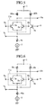
- Fig. 1 is a schematic circuit diagram showing the structure of a prior art frequency converter.
- reference numeral 1 denotes a power supply terminal to which a DC voltage Vcc is applied
- reference numerals 2a and 2b denote transistors each used for input of a local oscillation (LO) signal
- reference numeral 3a denotes a reference transistor
- reference numeral 5 denotes a constant current source
- reference numerals 6a and 6b denote load resistors
- reference numeral 7a denotes a radio frequency (RF) signal input terminal
- reference numerals 8a and 8b denote local oscillation (LO) signal input terminals
- reference numeral 9 denotes a reference bias terminal
- reference numerals 10a and 10b denote output terminals
- reference numeral 11a denotes a transistor pair that consists of the LO signal input transistors 2a and 2b
- reference numeral 14 denotes a transistor for input of a radio frequency (RF) signal.
- RF radio frequency
- a DC voltage Vcc which is applied to the power supply terminal 1 of the prior art frequency converter as shown in Fig. 1, is then applied to the transistor pair 11a that consists of the two LO signal input transistors 2a and 2b and the RF signal input transistor 14, and the reference transistor 3a by way of the two load resistors 6a and 6b, respectively.
- the constant current source 5 supplies a constant current to a parallel circuit that consists of the transistor pair 11a and the reference transistor 3a by way of the RF signal input transistor 14.
- a bias current is supplied to the reference transistor 3a by way of the reference bias terminal 9.
- the RF signal input transistor 14 amplifies an RF signal that is applied to the base terminal thereof by way of the RF signal input terminal 7a.
- the LO signal input transistor 2a amplifies an LO signal of positive phase that is applied to the base terminal thereof by way of the LO signal input terminal 8a
- the other LO signal input transistor 2b amplifies another LO signal of negative phase that is applied to the base terminal thereof by way of the other LO signal input terminal 8b.
- the transistor pair 11a in which the collector terminals of these transistors are commonly connected to each other and the emitter terminals of these transistors are commonly connected to each other generates a signal having a frequency that is two times as high as that of the LO signals.
- the sum of an electric current that flows through the transistor pair 11a and an electric current that flows through the reference transistor 3a is equal to an electric current that flows through the RF signal input transistor 14, and is therefore equal to an electric current output from the constant current source 5 connected to the emitter terminal of the RF signal input transistor 14. Because while the signal generated by the transistor pair 11a and having a frequency that is two times as high as that of the LO signals changes the electric current that flows through the transistor pair 11a, the RF signal input transistor 14 operates from the constant current from the constant current source 5, a signal having a phase opposite to that of a change in the electric current that flows through the transistor pair 11a flows through the reference transistor 3a. Therefore, the prior art frequency converter as shown in Fig.
- 1 serves as an even order harmonics frequency converter having a gain, which mixes the RF signal amplified by the RF signal input transistor 14, the signal generated by the transistor pair 11a and having a frequency that is two times as high as that of the LO signals, and the negative-phase signal that flows through the reference transistor 3a, and outputs the mixed signal as a differential signal by way of the output terminals 10a and 10b respectively connected to the load resistors 10a and 10b.
- a problem with the prior art frequency converter constructed as previously mentioned is that the saturation and distortion characteristics of the frequency converter are determined by the large signal characteristic of the RF signal input transistor 14 that is an active element, and therefore the saturation and distortion characteristics cannot be easily improved and degrade remarkably when the prior art frequency converter operates from a low voltage and/or a low current.
- the present invention is proposed to solve the above-mentioned problem, and it is therefore an object of the present invention to provide a frequency converter that can exhibit an excellent saturation characteristic and an excellent distortion characteristic even when operating from a low voltage and/or a low current because of a resistor that is a passive element and is disposed in an RF signal input circuit instead of a transistor.
- a frequency converter including: a transistor pair having a first transistor and a second transistor respectively having first terminals commonly connected to each other and second terminals commonly connected to each other, the commonly-connected first terminals (referred to as a first common terminal from here on) being connected to a power supply terminal by way of a first passive element; a third transistor having a first terminal connected to the power supply terminal by way of a second passive element, and a second terminal connected to the commonly-connected second terminals (referred to as a second common terminal from here on) of the first and second transistors of the transistor pair; a third passive element having an end connected to the second common terminal of the transistor pair, and another end directly or indirectly grounded; and an output terminal connected to the first common terminal of the transistor pair, a first signal being applied to a third terminal of the first transistor, a second signal having a phase opposite to that of the first signal being applied to a third terminal of the second transistor, a third signal being applied to the second common terminal of the transistor pair, and a
- the frequency converter can exhibit an excellent saturation characteristic and an excellent distortion characteristic even when operating from a low voltage and/or a low current.
- the frequency converter in accordance with the present invention can include another output terminal connected to the first terminal of the third transistor.
- the frequency converter can remove the in-phase component included in unnecessary frequency components of the output signal.
- the first to third passive elements are resistors.
- the first to third passive elements are inductors.
- the frequency converter in accordance with the present invention can include a constant current source connected between the other end of the third passive element and a ground.
- the frequency converter can have a voltage conversion gain.
- each of the first to third transistors is a bipolar junction transistor having a collector terminal as the first terminal, an emitter terminal as the second terminal, and a base terminal as the third terminal.
- each of the first to third transistors is a field effect transistor having a drain terminal as the first terminal, a source terminal as the second terminal, and a gate terminal as the third terminal.
- a frequency converter including: a first transistor pair having a first transistor and a second transistor respectively having first terminals commonly connected to each other and second terminals commonly connected to each other, the commonly-connected first terminals (referred to as a first common terminal from here on) being connected to a power supply terminal by way of a first passive element; a third transistor having a first terminal directly or indirectly connected to the power supply terminal, and a second terminal connected to the commonly-connected second terminals (referred to as a second common terminal from here on) of the first and second transistors of the first transistor pair; a second passive element having an end connected to the second common terminal of the first transistor pair, and another end directly or indirectly grounded; a first output terminal connected to the first common terminal of the first transistor pair; a second transistor pair having a fourth transistor and a fifth transistor respectively having first terminals commonly connected to each other and second terminals commonly connected to each other, the commonly-connected first terminals (referred to as a first common terminal from here on) being connected to the power supply terminal
- the frequency converter can exhibit an excellent saturation characteristic and an excellent distortion characteristic even when operating from a low voltage and/or a low current.
- the frequency converter can further suppress the odd order harmonics of the third signal, and a mixture of even order components of the first signal and even order components of the third signal.
- the first terminal of the third transistor is connected to the power supply terminal by way of the fifth passive element
- the first terminal of the sixth transistor is connected to the power supply terminal by way of the sixth passive element.
- the first terminal of the third transistor is connected to the second output terminal and is also connected to the power supply terminal by way of the third passive element
- the first terminal of the sixth transistor is connected to the first output terminal and is also connected to the power supply terminal by way of the first passive element
- the circuit structure of the frequency converter can be simplified, and the second order component of the first signal can be further suppressed.
- the first to fourth passive elements are resistors.
- the first to fourth passive elements are inductors.
- each transistor included in the frequency converter can be made to operate in a linear region without increase in a voltage that appears between the first and second terminals of each transistor.
- the first to sixth passive elements are resistors.
- the first to sixth passive elements are inductors.
- the frequency converter in accordance with the present invention can include a constant current source connected between the other ends of the third and fourth passive element and a ground.
- the frequency converter can have a voltage conversion gain.
- the frequency converter in accordance with the present invention can include a resistor connected between the other ends of the third and fourth passive element and a ground. As a result, variations in the performance of the frequency converter due to temperature variations can be prevented because no constant current source is used.
- each of the first to sixth transistors is a bipolar junction transistor having a collector terminal as the first terminal, an emitter terminal as the second terminal, and a base terminal as the third terminal.
- each of the first to sixth transistors is a field effect transistor having a drain terminal as the first terminal, a source terminal as the second terminal, and a gate terminal as the third terminal.
- Fig. 2 is a schematic circuit diagram showing the structure of a frequency converter in accordance with embodiment 1 of the present invention.
- reference numeral 1 denotes a power supply terminal to which a DC voltage Vcc is applied
- reference numerals 2a and 2b denote transistors (i.e., first and second transistors) each used for input of a local oscillation (LO) signal
- reference numeral 3a denotes a reference transistor (i.e., a third transistor) used for input of a reference signal
- reference numeral 4a denotes a resistor (i.e., a third passive element) used for input of a radio frequency (RF) signal
- reference numeral 5 denotes a constant current source
- reference numerals 6a and 6b denote load resistors (i.e., first and second passive elements)
- reference numeral 7a denotes a radio frequency (RF) signal input terminal
- reference numerals 8a and 8b denote local oscillation (LO) signal input terminals
- the LO signal input transistors 2a and 2b which constitute the transistor pair 11a, have collector terminals (i.e., first terminals) that are commonly connected to each other, and emitter terminals (i.e., second terminals) that are commonly connected to each other, respectively.
- the RF signal input terminal 7a, one end of the RF signal input resistor 4a and an emitter terminal of the reference transistor 3a are connected to the emitter terminals (referred to as a common emitter terminal (i.e., a second common terminal) from here on) of the LO signal input transistors 2a and 2b, which are commonly connected to each other.
- Another end of the RF signal input resistor 4a is connected to a ground by way of the constant current source 5.
- the collector terminals (referred to as a common collector terminal (i.e., a first common terminal) from here on) of the LO signal input transistors 2a and 2b, which are commonly connected to each other, are connected to the output terminal 10a and one end of the load resistor 6a, and another end of the load resistor 6a is connected to the power supply terminal 1.
- One end of the other load resistor 6b is connected to the power supply terminal 1, and another end of the other load resistor 6b is connected to a collector terminal of the reference transistor 3a.
- base terminals of the LO signal input transistors 2a and 2b are connected to the LO signal input terminals 8a and 8b, respectively, and a base terminal of the reference transistor 3a is connected to the reference bias terminal 9.
- the frequency converter in accordance with this embodiment 1 mixes an RF signal (i.e., a third signal) applied thereto by way of the RF signal input terminal 7a and a signal having a frequency that is two times as high as those of an LO signal of positive phase (i.e., a first signal) applied thereto by way of the LO signal input terminal 8a and another LO signal of negative phase (i.e., a second signal) applied thereto by way of the other LO signal input terminal 8b, the signal being generated by the transistor pair 11a from the LO signal of positive phase and the other LO signal of negative phase, so as to generate a mixed signal, and then outputs the mixed signal by way of the output terminal 10a.
- an RF signal i.e., a third signal
- a signal having a frequency that is two times as high as those of an LO signal of positive phase i.e., a first signal
- another LO signal of negative phase i.e., a second signal
- a DC voltage Vcc applied to the power supply terminal 1 of the frequency converter is then applied to both the transistor pair 11a, which consists of the LO signal input transistors 2a and 2b, and the reference transistor 3a by way of the two load resistors 6a and 6b.
- Constant currents are supplied from the constant current source 5 to the LO signal input transistors 2a and 2b and the reference transistor 3a, respectively.
- a bias current i.e., a reference signal
- the LO signal input transistor 2a amplifies the LO signal of positive phase applied to the base terminal thereof by way of the LO signal input terminal 8a.
- the LO signal input transistor 2b amplifies the other LO signal of negative phase applied to the base terminal thereof by way of the LO input terminal 8b.
- the transistor pair 11a in which the collector terminals of those transistors 2a and 2b are commonly connected to each other and the emitter terminals of those transistors 2a and 2b are also commonly connected to each other generates a signal having a frequency that is two times as high as that of the two LO signals.
- the sum of an electric current that flows through the transistor pair 11a and an electric current that flows through the reference transistor 3a is equal to an electric current that flows through the RF signal input resistor 4a, i.e., an electric current output from the constant current source 5. Therefore, because the signal having a frequency that is two times as high as that of the LO signals and generated by the transistor pair 11a causes a change in the electric current that flows through the transistor pair 11a while the electric current that flows in the entire parallel circuit consists of the transistor pair 11a and the reference transistor 3a, i.e., the electric current that flows through the RF signal input resistor 4a is maintained constant by the constant current.
- the frequency converter in accordance with this embodiment 1 serves as an even order harmonics frequency converter that outputs, as an intermediate frequency (IF) signal, a mixed signal (e.g., a signal having a frequency of (f RF -2f L0 ), where f RF is the frequency of the RF signal and f L0 is the frequency of the LO signals), into which the RF signal, the positive-phase signal having a frequency that is two times as high as that of the LO signals and generated by the transistor pair 11 and the negative-phase signal flowing through the reference transistor 3a are mixed, by way of the output terminal 10a connected between the load resistor 6a and the common collector terminal of the transistor pair 11a.
- IF intermediate frequency
- a mixed signal e.g., a signal having a frequency of (f RF -2f L0 ), where f RF is the frequency of the RF signal and f L0 is the frequency of the LO signals
- the frequency converter in accordance with this embodiment 1 can thus exhibit a high saturation characteristic and a high distortion characteristic because it does not use, as the RF signal input element, any transistor that is an active element.
- the frequency converter in accordance with this embodiment 1 can also have a voltage conversion gain.
- the frequency converter in accordance with this embodiment 1 is not limited to the above-mentioned downconverter and can be alternatively an upconverter that outputs a mixed signal into which an IF signal applied to the RF signal input terminal instead of the RF signal, the positive-phase signal having a frequency that is two times as high as that of the LO signals and generated by the transistor pair 11 and the negative-phase signal flowing through the reference transistor 3a are mixed, e.g., an RF signal having a frequency of (f IF +2f L0 ) (f IF is the frequency of the IF signal) by way of the output terminal 10a.
- this embodiment offers an advantage of being able to exhibit a high saturation characteristic and a high distortion characteristic.
- Fig. 3 is a schematic circuit diagram showing the structure of a frequency converter in accordance with a variant of embodiment 1.
- the transistor pair 11a consists of two field-effect transistors 20a and 20b, and a reference field-effect transistor 30a used for input of a reference signal is disposed instead of the reference transistor 3a.
- the collector terminal, emitter terminal, and base terminal of each bipolar junction transistor of Fig. 2 are replaced by the drain terminal, source terminal, and gate terminal of each field-effect transistor.
- Fig. 4 is a schematic circuit diagram showing the structure of a frequency converter in accordance with another variant of embodiment 1.
- the load resistors 6a and 6b, and the RF signal input resistor 4a are replaced by inductors 60a, 60b, and 40a, respectively.
- each transistor included in the frequency converter can be made to operate in a linear region without increase in the collector-emitter voltage of each. transistor.
- All the resistors of the frequency converter need not be replaced by inductors. For example, as shown in Figs. 5 and 6, only either of the load resistors 6a and 6b and the RF signal input resistor 4a may be replaced by inductors.
- Fig. 7 is a schematic circuit diagram showing the structure of a frequency converter in accordance with another variant of embodiment 1.
- the constant current source 5 is omitted, and the other end of the RF signal input resistor 4a is connected directly with the ground.
- the frequency converter does not include the constant current source 5, because the electric current flowing through the entire parallel circuit that consists of the transistor pair 11a and the reference transistor 3a is maintained constant by both the DC voltage Vcc applied to the power supply terminal 1 and the RF signal input resistor 4a, the same advantage is provided.
- Fig. 8 is a schematic circuit diagram showing the structure of a frequency converter in accordance with embodiment 2 of the present invention.
- the same reference numerals as shown in Fig. 2 denotes the same components as those of the frequency converter in accordance with above-mentioned embodiment 1 or like components, and therefore the explanation of those components will be omitted hereafter.
- reference numeral 10b denotes a second output terminal connected between a load resistor 6b and a collector terminal of a reference transistor 3b.
- the frequency converter in accordance with this embodiment 2 operates basically in the same way that that in accordance with above-mentioned embodiment 1 does. Next, only a characterized operation of the frequency converter in accordance with this embodiment 2 will be explained.
- the frequency converter in accordance with this embodiment 2 outputs, as an output signal, a differential signal by way of a differential terminal pair that consists of a first output terminal 10a and the second output terminal 10b.
- the frequency converter in accordance with this embodiment 2 can remove the in-phase component included in unnecessary frequency components of the output signal.
- a transistor pair 11a consists of two field-effect transistors 20a and 20b, and a reference field-effect transistor 30a used for input of a reference signal is disposed instead of a reference transistor 3a, as in the case as shown in Fig. 3.
- the collector terminal, emitter terminal, and base terminal of each bipolar junction transistor of Fig. 8 are replaced by the drain terminal, source terminal, and gate terminal of each field-effect transistor.
- load resistors 6a and 6b, and an RF signal input resistor 4a are replaced by inductors 60a, 60b, and 40a, respectively, as in the case as shown in Fig. 4.
- inductors 60a, 60b, and 40a are replaced by inductors.
- a constant current source 5 is omitted, and an end of the RF signal input resistor 4a is connected directly with a ground, as in the case as shown in Fig. 7.
- Fig. 9 is a schematic circuit diagram showing the structure of a frequency converter in accordance with embodiment 3 of the present invention.
- the same reference numerals as shown in Fig. 8 denotes the same components as those of the frequency converter in accordance with above-mentioned embodiment 2 or like components, and therefore the explanation of those components will be omitted hereafter.
- Fig. 8 the same reference numerals as shown in Fig. 8 denotes the same components as those of the frequency converter in accordance with above-mentioned embodiment 2 or like components, and therefore the explanation of those components will be omitted hereafter.
- reference numerals 2c and 2d denote LO signal input transistors (i.e., fourth and fifth transistors) each used for input of a local oscillation (LO) signal
- reference numeral 3b denotes a second reference transistor (i.e., a sixth transistor) used for input of a reference signal
- reference numeral 4b denotes a second RF signal input resistor (i.e., a fourth passive element) used for input of a radio frequency (RF) signal
- reference numerals 6c and 6d denote load resistors
- reference numeral 7b denotes a second radio frequency (RF) signal input terminal
- reference numeral 11b denotes a second transistor pair that consists of the LO signal input transistors 2c and 2d.
- two parallel circuits are connected in parallel between a power supply terminal 1 and a ground.
- a first RF signal input terminal 7a is connected between a first RF signal input resistor 4a (i.e., a second passive element) and a common emitter terminal of a first transistor pair 11a.
- the second RF signal input terminal 7b is connected between the second RF signal input resistor 4b and a common emitter terminal of the second transistor pair 11b.
- An LO signal input terminal 8a is connected to a base terminal of an LO signal input transistor 2a of the first transistor pair 11a and a base terminal of the LO signal input transistor 2d of the second transistor pair 11b.
- another LO signal input terminal 8b is connected to a base terminal of another LO signal input transistor 2b of the first transistor pair 11a and a base terminal of the other LO signal input transistor 2c of the second transistor pair 11b.
- a first output terminal 10a is connected between a load resistor 6a (i.e., a first passive element) and a common collector terminal of the first transistor pair 11a.
- a second output terminal 10b is connected between the load resistor 6c (i.e., a third passive element) and a common collector terminal of the second transistor pair 11b.
- a first reference transistor 3a and the second reference transistor 3b have base terminals connected commonly with a reference bias terminal 9, collector terminals connected to the power supply terminal 1 by way of the load resistors 6b and 6d (i.e., fifth and sixth passive elements), respectively, and emitter terminals connected to the common emitter terminals of the first and second transistor pairs 11a and 11b, respectively.
- the frequency converter in accordance with this embodiment 3 operates basically in the same way that that in accordance with above-mentioned embodiment 2 does. Next, only a characterized operation of the frequency converter in accordance with this embodiment 3 will be explained.
- An RF signal (i.e., a third signal) of positive phase is applied to the common emitter terminal of the first transistor pair 11a by way of the first RF signal input terminal 7a, and another RF signal (i.e., a fourth signal) of negative phase is applied to the common emitter terminal of the second transistor pair 11b by way of the second RF signal input terminal 7b.
- the frequency converter in accordance with this embodiment 3 serves as an even order harmonics frequency converter that outputs, as an intermediate frequency (IF) signal, a differential signal consisting of both a mixed signal (e.g., a signal having a frequency of (f RF -2f L0 ), where f RF is the frequency of the RF signals and f L0 is the frequency of the LO signals) , into which the RF signal of positive phase, a positive-phase signal having a frequency that is two times as high as that of the LO signals and generated by the first transistor pair 11a and a negative-phase signal flowing through the first reference transistor 3a are mixed, and a mixed signal (e.g., a signal having a frequency of (f RF -2f L0 )), into which the other RF signal of negative phase, a positive-phase signal having a frequency that is two times as high as that of the LO signals and generated by the second transistor pair 11b and a negative-phase signal flowing through the second reference transistor 3b are mixed, by way of
- the frequency converter in accordance with this embodiment 3 thus has a balanced-type structure, receives the RF signal of positive phase and the other RF signal of negative phase, and outputs a differential signal that consists of mixed signals respectively including the RF signal of positive phase and the other RF signal of negative phase, the same advantage as offered by above-mentioned embodiment 1 is provided.
- the frequency converter in accordance with this embodiment 3 can further suppress the odd order harmonics of the RF signals, and a mixture of even order components of the LO signals and even order components of the RF signals, as compared with that of above-mentioned embodiment 1.
- the frequency converter in accordance with this embodiment 3 facilitates an output of a mixture wave of the second order components of the LO signals and the first order components of the RF signals, which can be general output signals from a harmonic mixer, and suppresses unnecessary spurious components, the structure of a filter circuit intended for reduction of spurious components and connected as an output stage of the frequency converter can be simplified.
- the frequency converter in accordance with this embodiment 3 is not limited to the above-mentioned downconverter and can be alternatively an upconverter that outputs a differential signal consisting of both a mixed signal into which an IF signal of positive phase applied to the first RF signal input terminal instead of the RF signal of positive, the positive-phase signal having a frequency that is two times as high as that of the LO signals and generated by the first transistor pair 11a and the negative-phase signal flowing through the first reference transistor 3a are mixed, e.g., an RF signal having a frequency of (f IF +2f L0 ) (f IF is the frequency of the IF signal) and a mixed signal into which another IF signal of negative phase applied to the second RF signal input terminal instead of the other RF signal of negative phase, the positive-phase signal having a frequency that is two times as high as that of the LO signals and generated by the second transistor pair 11b and the negative-phase signal flowing through the second reference transistor 3b are mixed, e.g., an
- Fig. 10 is a schematic circuit diagram showing the structure of a frequency converter in accordance with a variant of embodiment 3.
- the first transistor pair 11a consists of two field-effect transistors 20a and 20b and the second transistor pair 11b consists of two field-effect transistors 20c and 20d, and reference field-effect transistors 30a and 30b each used for input of a reference signal are disposed instead of the first and second reference transistors 3a and 3b.
- the collector terminal, emitter terminal, and base terminal of each bipolar junction transistor of Fig. 9 are replaced by the drain terminal, source terminal, and gate terminal of each field-effect transistor.
- Fig. 11 is a schematic circuit diagram showing the structure of a frequency converter in accordance with another variant of embodiment 3.
- the load resistors 6a to 6d, and the RF signal input resistors 4a and 4b are replaced by inductors 60a to 60d, and 40a and 40b, respectively.
- all the resistors of the frequency converter need not be replaced by inductors.
- only either of the load resistors 6a to 6d and the RF signal input resistors 4a and 4b may be replaced by inductors.
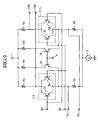
- Fig. 14 is a schematic circuit diagram showing the structure of a frequency converter in accordance with another variant of embodiment 3.
- a constant current source 5 is omitted, and the other ends of the RF signal input resistors 4a and 4b are connected directly with the ground.
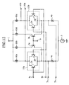
- Fig. 15 is a schematic circuit diagram showing the structure of a frequency converter in accordance with another variant of embodiment 3.
- the constant current source 5 is replaced by a resistor 12.
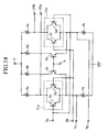
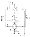
- Fig. 16 is a schematic circuit diagram showing the structure of a frequency converter in accordance with embodiment 4 of the present invention.
- the same reference numerals as shown in Fig. 9 denotes the same components as those of the frequency converter in accordance with above-mentioned embodiment 3 or like components, and therefore the explanation of those components will be omitted hereafter.
- the frequency converter in accordance with this embodiment 4 differs from that in accordance with above-mentioned embodiment 3 in that the load resistors 6b and 6d (i.e., fifth and sixth passive elements) as shown in Fig. 9 are omitted. In other words, the collector terminals of first and second reference transistors 3a and 3b are connected directly with a power supply terminal 1.
- the load resistors 6b and 6d i.e., fifth and sixth passive elements
- the frequency converter in accordance with this embodiment 4 operates in the same way that that in accordance with above-mentioned embodiment 3 does.
- the frequency converter in accordance with this embodiment 4 outputs a differential signal by way of first and second output terminals 10a and 10b respectively connected to load resistors 6a and 6c, like that in accordance with above-mentioned embodiment 3.
- this embodiment 4 can provide the same advantage as offered by above-mentioned embodiment 3, and the circuit structure of the frequency converter can be simplified.
- each of first and second transistor pairs 11a and 11b consists of two field-effect transistors, as in the case shown in Fig. 10, and reference field-effect transistors each used for input of a reference signal are disposed instead of the first and second reference transistors 3a and 3b.
- the collector terminal, emitter terminal, and base terminal of each bipolar junction transistor are replaced by the drain terminal, source terminal, and gate terminal of each field-effect transistor.
- the load resistors 6a to 6d, and RF signal input resistors 4a and 4b are replaced by inductors, respectively.
- each transistor included in the frequency converter can be made to operate in a linear region without increase in the collector-emitter voltage of each transistor.
- All the resistors of the frequency converter need not be replaced by inductors, as in the cases shown in Figs. 12 and 13, only either of the load resistors 6a to 6d and the RF signal input resistors 4a and 4b may be replaced by inductors.
- a constant current source 5 is omitted and other ends of the RF signal input resistors 4a and 4b are connected directly with a ground.
- the frequency converter does not include the constant current source 5 because an electric current flowing through a parallel circuit that consists of the first transistor pair 11a and the first reference transistor 3a is maintained constant by both the DC voltage Vcc applied to the power supply terminal 1 and the first RF signal input resistor 4a and an electric current flowing through another parallel circuit that consists of the second transistor pair 11b and the second reference transistor 3b is maintained constant by both the DC voltage Vcc applied to the power supply terminal 1 and the second RF signal input resistor 4b, the same advantage is provided.
- the constant current source 5 is replaced by a resistor.
- variations in the performance of the frequency converter due to temperature variations of the constant current source 5, which is usually constructed of a transistor, can be prevented.
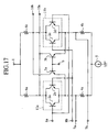
- Fig. 17 is a schematic circuit diagram showing the structure of a frequency converter in accordance with embodiment 5 of the present invention.
- the same reference numerals as shown in Fig. 16 denotes the same components as those of the frequency converter in accordance with above-mentioned embodiment 4 or like components, and therefore the explanation of those components will be omitted hereafter.
- the frequency converter in accordance with this embodiment 5 has a circuit structure similar to that of the frequency converter in accordance with above-mentioned embodiment 4, the frequency converter in accordance with this embodiment 5 differs from that in accordance with embodiment 4 in that a collector terminal of a first reference transistor 3a is connected to a second output terminal 10b, i.e., between a load resistor 6c and a common collector terminal of a second transistor pair 11b, and a collector terminal of a second reference transistor 3b is connected to a first output terminal 10a, i.e., between a load resistor 6a and a common collector terminal of a first transistor pair 11a.
- the frequency converter in accordance with this embodiment 5 operates basically in the same way that that in accordance with above-mentioned embodiment 4 does. Next, only a characterized operation of the frequency converter in accordance with this embodiment 5 will be explained.
- this embodiment 5 provides the same advantage as offered by above-mentioned embodiment 4, and an advantage of further suppressing the appearance of the second order components of the LO signals at the first and second output terminals 10a and 10b.
- each of first and second transistor pairs 11a and 11b consists of two field-effect transistors, as in the case shown in Fig. 10, and reference field-effect transistors each used for input of a reference signal are disposed instead of the first and second reference transistors 3a and 3b.
- the collector terminal, emitter terminal, and base terminal of each bipolar junction transistor are replaced by the drain terminal, source terminal, and gate terminal of each field-effect transistor.
- the load resistors 6a to 6d, and RF signal input resistors 4a and 4b are replaced by inductors, respectively.
- each transistor included in the frequency converter can be made to operate in a linear region without increase in the collector-emitter voltage of each transistor.
- All the resistors of the frequency converter need not be replaced by inductors, as in the cases shown in Figs. 12 and 13, only either of the load resistors 6a to 6d and the RF signal input resistors 4a and 4b may be replaced by inductors.
- a constant current source 5 is omitted and other ends of the RF signal input resistors 4a and 4b are connected directly with a ground.
- the frequency converter does not include the constant current source 5 because an electric current flowing through an entire parallel circuit that consists of the first transistor pair 11a and the first reference transistor 3a is maintained constant by both the DC voltage Vcc applied to the power supply terminal 1 and the first RF signal input resistor 4a and an electric current flowing through an entire parallel circuit that consists of the second transistor pair 11b and the second reference transistor 3b is maintained constant by both the DC voltage Vcc applied to the power supply terminal 1 and the second RF signal input resistor 4b, the same advantage is provided.
- the constant current source 5 is replaced by a resistor.
- variations in the performance of the frequency converter due to temperature variations of the constant current source 5, which is usually constructed of a transistor, can be prevented.
- the frequency converter in accordance with the present invention is suitable for multiplying the frequency of a high-frequency signal, such as a UHF, microwave, or millimeter wave, by a certain factor, or mixing high-frequency signals with each other in a wideband communication terminal or the like that conforms to a communication system such as a WCDMA system.
- a high-frequency signal such as a UHF, microwave, or millimeter wave
Landscapes
- Engineering & Computer Science (AREA)
- Power Engineering (AREA)
- Amplifiers (AREA)
- Superheterodyne Receivers (AREA)
Abstract
A frequency converter includes a transistor pair (11a)
having first and second transistors (2a and 2b) respectively
having collector terminals commonly connected to each other
and emitter terminals commonly connected to each other, the
collector terminals being connected to a power supply terminal
(1) by way of a resistor (6a), another transistor (3a) having
a collector terminal connected to the power supply terminal
by way of another resistor (6b) and an emitter terminal
connected to the emitter terminals of the transistor pair,
another resistor (4a) having an end connected to the emitter
terminals of the transistor pair, and another end grounded by
way of a constant current source (5), and an output terminal
(1) connected to the collector terminals of the transistor pair.
The frequency converter can thus exhibit an excellent
saturation characteristic and an excellent distortion
characteristic even when operating from a low voltage and/or
a low current.
Description
The present invention relates to a frequency converter
that multiplies the frequency of a high-frequency signal, such
as a UHF, microwave, or millimeter wave, by a certain factor,
or mixes high-frequency signals with each other in a wideband
communication terminal or the like that conforms to a
communication system such as a WCDMA system.
Fig. 1 is a schematic circuit diagram showing the
structure of a prior art frequency converter. In the figure,
reference numeral 1 denotes a power supply terminal to which
a DC voltage Vcc is applied, reference numerals 2a and 2b denote
transistors each used for input of a local oscillation (LO)
signal, reference numeral 3a denotes a reference transistor,
reference numeral 5 denotes a constant current source,
reference numerals 6a and 6b denote load resistors, reference
numeral 7a denotes a radio frequency (RF) signal input terminal,
reference numerals 8a and 8b denote local oscillation (LO)
signal input terminals, reference numeral 9 denotes a
reference bias terminal, reference numerals 10a and 10b denote
output terminals, reference numeral 11a denotes a transistor
pair that consists of the LO signal input transistors 2a and
2b, and reference numeral 14 denotes a transistor for input
of a radio frequency (RF) signal. As shown in Fig. 1, in the
prior art frequency converter, an RF signal is applied to the
emitter-grounded RF signal input transistor 14.
Next, a description will be made as to an operation of
the prior art frequency converter.
A DC voltage Vcc, which is applied to the power supply
terminal 1 of the prior art frequency converter as shown in
Fig. 1, is then applied to the transistor pair 11a that consists
of the two LO signal input transistors 2a and 2b and the RF
signal input transistor 14, and the reference transistor 3a
by way of the two load resistors 6a and 6b, respectively. The
constant current source 5 supplies a constant current to a
parallel circuit that consists of the transistor pair 11a and
the reference transistor 3a by way of the RF signal input
transistor 14. A bias current is supplied to the reference
transistor 3a by way of the reference bias terminal 9.
The RF signal input transistor 14 amplifies an RF signal
that is applied to the base terminal thereof by way of the RF
signal input terminal 7a. On the other hand, the LO signal
input transistor 2a amplifies an LO signal of positive phase
that is applied to the base terminal thereof by way of the LO
signal input terminal 8a, and the other LO signal input
transistor 2b amplifies another LO signal of negative phase
that is applied to the base terminal thereof by way of the other
LO signal input terminal 8b. Thus, because the LO signal of
positive phase and the other LO signal of negative phase are
applied to the base terminals of the LO signal input transistors
2a and 2b, respectively, the transistor pair 11a in which the
collector terminals of these transistors are commonly
connected to each other and the emitter terminals of these
transistors are commonly connected to each other generates a
signal having a frequency that is two times as high as that
of the LO signals.
The sum of an electric current that flows through the
transistor pair 11a and an electric current that flows through
the reference transistor 3a is equal to an electric current
that flows through the RF signal input transistor 14, and is
therefore equal to an electric current output from the constant
current source 5 connected to the emitter terminal of the RF
signal input transistor 14. Because while the signal
generated by the transistor pair 11a and having a frequency
that is two times as high as that of the LO signals changes
the electric current that flows through the transistor pair
11a, the RF signal input transistor 14 operates from the
constant current from the constant current source 5, a signal
having a phase opposite to that of a change in the electric
current that flows through the transistor pair 11a flows
through the reference transistor 3a. Therefore, the prior art
frequency converter as shown in Fig. 1 serves as an even order
harmonics frequency converter having a gain, which mixes the
RF signal amplified by the RF signal input transistor 14, the
signal generated by the transistor pair 11a and having a
frequency that is two times as high as that of the LO signals,
and the negative-phase signal that flows through the reference
transistor 3a, and outputs the mixed signal as a differential
signal by way of the output terminals 10a and 10b respectively
connected to the load resistors 10a and 10b.
A problem with the prior art frequency converter
constructed as previously mentioned is that the saturation and
distortion characteristics of the frequency converter are
determined by the large signal characteristic of the RF signal
input transistor 14 that is an active element, and therefore
the saturation and distortion characteristics cannot be easily
improved and degrade remarkably when the prior art frequency
converter operates from a low voltage and/or a low current.
The present invention is proposed to solve the
above-mentioned problem, and it is therefore an object of the
present invention to provide a frequency converter that can
exhibit an excellent saturation characteristic and an
excellent distortion characteristic even when operating from
a low voltage and/or a low current because of a resistor that
is a passive element and is disposed in an RF signal input
circuit instead of a transistor.
In accordance with the present invention, there is
provided a frequency converter including: a transistor pair
having a first transistor and a second transistor respectively
having first terminals commonly connected to each other and
second terminals commonly connected to each other, the
commonly-connected first terminals (referred to as a first
common terminal from here on) being connected to a power supply
terminal by way of a first passive element; a third transistor
having a first terminal connected to the power supply terminal
by way of a second passive element, and a second terminal
connected to the commonly-connected second terminals
(referred to as a second common terminal from here on) of the
first and second transistors of the transistor pair; a third
passive element having an end connected to the second common
terminal of the transistor pair, and another end directly or
indirectly grounded; and an output terminal connected to the
first common terminal of the transistor pair, a first signal
being applied to a third terminal of the first transistor, a
second signal having a phase opposite to that of the first
signal being applied to a third terminal of the second
transistor, a third signal being applied to the second common
terminal of the transistor pair, and a reference signal being
applied to a third terminal of the third transistor.
As a result, the frequency converter can exhibit an
excellent saturation characteristic and an excellent
distortion characteristic even when operating from a low
voltage and/or a low current.
The frequency converter in accordance with the present
invention can include another output terminal connected to the
first terminal of the third transistor.
As a result, the frequency converter can remove the
in-phase component included in unnecessary frequency
components of the output signal.
In the frequency converter in accordance with the present
invention, the first to third passive elements are resistors.
In the frequency converter in accordance with the present
invention, the first to third passive elements are inductors.
As a result, each transistor included in the frequency
converter can be made to operate in a linear region without
increase in a voltage that appears between the first and second
terminals of each transistor.
The frequency converter in accordance with the present
invention can include a constant current source connected
between the other end of the third passive element and a ground.
As a result, the frequency converter can have a voltage
conversion gain.
In the frequency converter in accordance with the present
invention, each of the first to third transistors is a bipolar
junction transistor having a collector terminal as the first
terminal, an emitter terminal as the second terminal, and a
base terminal as the third terminal.
In the frequency converter in accordance with the present
invention, each of the first to third transistors is a field
effect transistor having a drain terminal as the first terminal,
a source terminal as the second terminal, and a gate terminal
as the third terminal.
In accordance with the present invention, there is
provided a frequency converter including: a first transistor
pair having a first transistor and a second transistor
respectively having first terminals commonly connected to each
other and second terminals commonly connected to each other,
the commonly-connected first terminals (referred to as a first
common terminal from here on) being connected to a power supply
terminal by way of a first passive element; a third transistor
having a first terminal directly or indirectly connected to
the power supply terminal, and a second terminal connected to
the commonly-connected second terminals (referred to as a
second common terminal from here on) of the first and second
transistors of the first transistor pair; a second passive
element having an end connected to the second common terminal
of the first transistor pair, and another end directly or
indirectly grounded; a first output terminal connected to the
first common terminal of the first transistor pair; a second
transistor pair having a fourth transistor and a fifth
transistor respectively having first terminals commonly
connected to each other and second terminals commonly
connected to each other, the commonly-connected first
terminals (referred to as a first common terminal from here
on) being connected to the power supply terminal by way of a
third passive element; a sixth transistor having a first
terminal directly or indirectly connected to the power supply
terminal, and a second terminal connected to the
commonly-connected second terminals (referred to as a second
common terminal from here on) of the fourth and fifth
transistors of the second transistor pair; a fourth passive
element having an end connected to the second common terminal
of the second transistor pair, and another end directly or
indirectly grounded; and a second output terminal connected
to the first common terminal of the second transistor pair,
a first signal being applied to third terminals of the first
and fifth transistors, a second signal having a phase opposite
to that of the first signal being applied to third terminals
of the second and fourth transistors, a third signal being
applied to the second common terminal of the first transistor
pair, a fourth signal having a phase opposite to that of the
third signal being applied to the second common terminal of
the second transistor pair, and a reference signal being
applied to third terminals of the third and sixth transistors.
As a result, the frequency converter can exhibit an
excellent saturation characteristic and an excellent
distortion characteristic even when operating from a low
voltage and/or a low current. The frequency converter can
further suppress the odd order harmonics of the third signal,
and a mixture of even order components of the first signal and
even order components of the third signal.
In the frequency converter in accordance with the present
invention can, the first terminal of the third transistor is
connected to the power supply terminal by way of the fifth
passive element, and the first terminal of the sixth transistor
is connected to the power supply terminal by way of the sixth
passive element.
In the frequency converter in accordance with the present
invention can, the first terminal of the third transistor is
connected to the second output terminal and is also connected
to the power supply terminal by way of the third passive element,
and the first terminal of the sixth transistor is connected
to the first output terminal and is also connected to the power
supply terminal by way of the first passive element.
As a result, the circuit structure of the frequency
converter can be simplified, and the second order component
of the first signal can be further suppressed.
In the frequency converter in accordance with the present
invention can, the first to fourth passive elements are
resistors.
In the frequency converter in accordance with the present
invention, the first to fourth passive elements are inductors.
As a result, each transistor included in the frequency
converter can be made to operate in a linear region without
increase in a voltage that appears between the first and second
terminals of each transistor.
In the frequency converter in accordance with the present
invention, the first to sixth passive elements are resistors.
In the frequency converter in accordance with the present
invention, the first to sixth passive elements are inductors.
As a result, each transistor included in the frequency
converter can be made to operate in a linear region without
increase in a voltage that appears between the first and second
terminals of each transistor.
The frequency converter in accordance with the present
invention can include a constant current source connected
between the other ends of the third and fourth passive element
and a ground.
As a result, the frequency converter can have a voltage
conversion gain.
The frequency converter in accordance with the present
invention can include a resistor connected between the other
ends of the third and fourth passive element and a ground.
As a result, variations in the performance of the frequency
converter due to temperature variations can be prevented
because no constant current source is used.
In the frequency converter in accordance with the present
invention, each of the first to sixth transistors is a bipolar
junction transistor having a collector terminal as the first
terminal, an emitter terminal as the second terminal, and a
base terminal as the third terminal.
In the frequency converter in accordance with the present
invention, each of the first to sixth transistors is a field
effect transistor having a drain terminal as the first terminal,
a source terminal as the second terminal, and a gate terminal
as the third terminal.
In order to explain the present invention in greater
detail, the preferred embodiments will be described below with
reference to the accompanying figures.
Fig. 2 is a schematic circuit diagram showing the
structure of a frequency converter in accordance with
embodiment 1 of the present invention. In the figure,
reference numeral 1 denotes a power supply terminal to which
a DC voltage Vcc is applied, reference numerals 2a and 2b denote
transistors (i.e., first and second transistors) each used for
input of a local oscillation (LO) signal, reference numeral
3a denotes a reference transistor (i.e., a third transistor)
used for input of a reference signal, reference numeral 4a
denotes a resistor (i.e., a third passive element) used for
input of a radio frequency (RF) signal, reference numeral 5
denotes a constant current source, reference numerals 6a and
6b denote load resistors (i.e., first and second passive
elements), reference numeral 7a denotes a radio frequency (RF)
signal input terminal, reference numerals 8a and 8b denote
local oscillation (LO) signal input terminals, reference
numeral 9 denotes a reference bias terminal to which the
reference signal is applied, reference numeral 10a denotes an
output terminal, and reference numeral 11a denotes a
transistor pair that consists of the LO signal input
transistors 2a and 2b each used for input of an LO signal.
As shown in Fig. 2, the LO signal input transistors 2a
and 2b, which constitute the transistor pair 11a, have
collector terminals (i.e., first terminals) that are commonly
connected to each other, and emitter terminals (i.e., second
terminals) that are commonly connected to each other,
respectively. The RF signal input terminal 7a, one end of the
RF signal input resistor 4a and an emitter terminal of the
reference transistor 3a are connected to the emitter terminals
(referred to as a common emitter terminal (i.e., a second common
terminal) from here on) of the LO signal input transistors 2a
and 2b, which are commonly connected to each other. Another
end of the RF signal input resistor 4a is connected to a ground
by way of the constant current source 5.
The collector terminals (referred to as a common
collector terminal (i.e., a first common terminal) from here
on) of the LO signal input transistors 2a and 2b, which are
commonly connected to each other, are connected to the output
terminal 10a and one end of the load resistor 6a, and another
end of the load resistor 6a is connected to the power supply
terminal 1. One end of the other load resistor 6b is connected
to the power supply terminal 1, and another end of the other
load resistor 6b is connected to a collector terminal of the
reference transistor 3a. Furthermore, base terminals of the
LO signal input transistors 2a and 2b are connected to the LO
signal input terminals 8a and 8b, respectively, and a base
terminal of the reference transistor 3a is connected to the
reference bias terminal 9.
Next, a description will be made as to an operation of
the frequency converter in accordance with embodiment 1 of the
present invention.
The frequency converter in accordance with this
embodiment 1 mixes an RF signal (i.e., a third signal) applied
thereto by way of the RF signal input terminal 7a and a signal
having a frequency that is two times as high as those of an
LO signal of positive phase (i.e., a first signal) applied
thereto by way of the LO signal input terminal 8a and another
LO signal of negative phase (i.e., a second signal) applied
thereto by way of the other LO signal input terminal 8b, the
signal being generated by the transistor pair 11a from the LO
signal of positive phase and the other LO signal of negative
phase, so as to generate a mixed signal, and then outputs the
mixed signal by way of the output terminal 10a.
A DC voltage Vcc applied to the power supply terminal
1 of the frequency converter is then applied to both the
transistor pair 11a, which consists of the LO signal input
transistors 2a and 2b, and the reference transistor 3a by way
of the two load resistors 6a and 6b. Constant currents are
supplied from the constant current source 5 to the LO signal
input transistors 2a and 2b and the reference transistor 3a,
respectively. A bias current (i.e., a reference signal) is
supplied to the base terminal of the reference transistor 3a
by way of the reference bias terminal 9.
The LO signal input transistor 2a amplifies the LO signal
of positive phase applied to the base terminal thereof by way
of the LO signal input terminal 8a. Similarly, the LO signal
input transistor 2b amplifies the other LO signal of negative
phase applied to the base terminal thereof by way of the LO
input terminal 8b. Thus, because the LO signal of positive
phase and the other LO signal of negative phase are applied
to the base terminals of the two LO signal input transistors
2a and 2b, respectively, the transistor pair 11a in which the
collector terminals of those transistors 2a and 2b are commonly
connected to each other and the emitter terminals of those
transistors 2a and 2b are also commonly connected to each other
generates a signal having a frequency that is two times as high
as that of the two LO signals.
The sum of an electric current that flows through the
transistor pair 11a and an electric current that flows through
the reference transistor 3a is equal to an electric current
that flows through the RF signal input resistor 4a, i.e., an
electric current output from the constant current source 5.
Therefore, because the signal having a frequency that is two
times as high as that of the LO signals and generated by the
transistor pair 11a causes a change in the electric current
that flows through the transistor pair 11a while the electric
current that flows in the entire parallel circuit consists of
the transistor pair 11a and the reference transistor 3a, i.e.,
the electric current that flows through the RF signal input
resistor 4a is maintained constant by the constant current.
source 5, a signal having a phase opposite to that of the change
in the electric current that flows through the transistor pair
11a flows through the reference transistor 3a. Therefore, the
frequency converter in accordance with this embodiment 1
serves as an even order harmonics frequency converter that
outputs, as an intermediate frequency (IF) signal, a mixed
signal (e.g., a signal having a frequency of (fRF-2fL0), where
fRF is the frequency of the RF signal and fL0 is the frequency
of the LO signals), into which the RF signal, the positive-phase
signal having a frequency that is two times as high as that
of the LO signals and generated by the transistor pair 11 and
the negative-phase signal flowing through the reference
transistor 3a are mixed, by way of the output terminal 10a
connected between the load resistor 6a and the common collector
terminal of the transistor pair 11a.
The frequency converter in accordance with this
embodiment 1 can thus exhibit a high saturation characteristic
and a high distortion characteristic because it does not use,
as the RF signal input element, any transistor that is an active
element. When the resistances of the load resistors 6a and
6b are suitably set and the electric current output from the
constant current source 5 is suitably set, the frequency
converter in accordance with this embodiment 1 can also have
a voltage conversion gain.
The frequency converter in accordance with this
embodiment 1 is not limited to the above-mentioned
downconverter and can be alternatively an upconverter that
outputs a mixed signal into which an IF signal applied to the
RF signal input terminal instead of the RF signal, the
positive-phase signal having a frequency that is two times as
high as that of the LO signals and generated by the transistor
pair 11 and the negative-phase signal flowing through the
reference transistor 3a are mixed, e.g., an RF signal having
a frequency of (fIF+2fL0) (fIF is the frequency of the IF signal)
by way of the output terminal 10a.
As mentioned above, because the frequency converter in
accordance with this embodiment 1 does not use, as the RF signal
input element, any transistor that is an active element, this
embodiment offers an advantage of being able to exhibit a high
saturation characteristic and a high distortion
characteristic.
Numerous variants can be made in this embodiment 1
mentioned above. Fig. 3 is a schematic circuit diagram showing
the structure of a frequency converter in accordance with a
variant of embodiment 1. In this variant, the transistor pair
11a consists of two field- effect transistors 20a and 20b, and
a reference field-effect transistor 30a used for input of a
reference signal is disposed instead of the reference
transistor 3a. In this case, the collector terminal, emitter
terminal, and base terminal of each bipolar junction
transistor of Fig. 2 are replaced by the drain terminal, source
terminal, and gate terminal of each field-effect transistor.
Fig. 4 is a schematic circuit diagram showing the
structure of a frequency converter in accordance with another
variant of embodiment 1. In this variant, the load resistors
6a and 6b, and the RF signal input resistor 4a are replaced
by inductors 60a, 60b, and 40a, respectively. As a result,
even though a DC bias electric current increases, each
transistor included in the frequency converter can be made to
operate in a linear region without increase in the
collector-emitter voltage of each. transistor. All the
resistors of the frequency converter need not be replaced by
inductors. For example, as shown in Figs. 5 and 6, only either
of the load resistors 6a and 6b and the RF signal input resistor
4a may be replaced by inductors.
Fig. 7 is a schematic circuit diagram showing the
structure of a frequency converter in accordance with another
variant of embodiment 1. In this variant, the constant current
source 5 is omitted, and the other end of the RF signal input
resistor 4a is connected directly with the ground. Thus, even
when the frequency converter does not include the constant
current source 5, because the electric current flowing through
the entire parallel circuit that consists of the transistor
pair 11a and the reference transistor 3a is maintained constant
by both the DC voltage Vcc applied to the power supply terminal
1 and the RF signal input resistor 4a, the same advantage is
provided.
Fig. 8 is a schematic circuit diagram showing the
structure of a frequency converter in accordance with
embodiment 2 of the present invention. In the figure, the same
reference numerals as shown in Fig. 2 denotes the same
components as those of the frequency converter in accordance
with above-mentioned embodiment 1 or like components, and
therefore the explanation of those components will be omitted
hereafter. Furthermore, in Fig. 8, reference numeral 10b
denotes a second output terminal connected between a load
resistor 6b and a collector terminal of a reference transistor
3b.
Next, a description will be made as to an operation of
the frequency converter in accordance with embodiment 2 of the
present invention.
The frequency converter in accordance with this
embodiment 2 operates basically in the same way that that in
accordance with above-mentioned embodiment 1 does. Next, only
a characterized operation of the frequency converter in
accordance with this embodiment 2 will be explained.
The frequency converter in accordance with this
embodiment 2 outputs, as an output signal, a differential
signal by way of a differential terminal pair that consists
of a first output terminal 10a and the second output terminal
10b. As a result, the frequency converter in accordance with
this embodiment 2 can remove the in-phase component included
in unnecessary frequency components of the output signal.
Numerous variants can be made in this embodiment 2, as
in the case of above-mentioned embodiment 1. A transistor pair
11a consists of two field- effect transistors 20a and 20b, and
a reference field-effect transistor 30a used for input of a
reference signal is disposed instead of a reference transistor
3a, as in the case as shown in Fig. 3. In this case, the
collector terminal, emitter terminal, and base terminal of
each bipolar junction transistor of Fig. 8 are replaced by the
drain terminal, source terminal, and gate terminal of each
field-effect transistor.
In another variant, load resistors 6a and 6b, and an RF
signal input resistor 4a are replaced by inductors 60a, 60b,
and 40a, respectively, as in the case as shown in Fig. 4. As
a result, even though a DC bias electric current increases,
each transistor included in the frequency converter can be made
to operate in a linear region without increase in the
collector-emitter voltage of each transistor. All resistors
of the frequency converter need not be replaced by inductors.
For example, as in the cases as shown in Figs. 5 and 6, only
either of the load resistors 6a and 6b and the RF signal input
resistor 4a may be replaced by inductors.
In another variant, a constant current source 5 is
omitted, and an end of the RF signal input resistor 4a is
connected directly with a ground, as in the case as shown in
Fig. 7. Thus, even when the frequency converter does not
include the constant current source 5, because an electric
current flowing through an entire parallel circuit that
consists of the transistor pair 11a and the reference
transistor 3a is maintained constant by both a DC voltage Vcc
applied to a power supply terminal 1 and the RF signal input
resistor 4a, the same advantage is provided.
Fig. 9 is a schematic circuit diagram showing the
structure of a frequency converter in accordance with
embodiment 3 of the present invention. In the figure, the same
reference numerals as shown in Fig. 8 denotes the same
components as those of the frequency converter in accordance
with above-mentioned embodiment 2 or like components, and
therefore the explanation of those components will be omitted
hereafter. In Fig. 9, reference numerals 2c and 2d denote LO
signal input transistors (i.e., fourth and fifth transistors)
each used for input of a local oscillation (LO) signal,
reference numeral 3b denotes a second reference transistor
(i.e., a sixth transistor) used for input of a reference signal,
reference numeral 4b denotes a second RF signal input resistor
(i.e., a fourth passive element) used for input of a radio
frequency (RF) signal, reference numerals 6c and 6d denote load
resistors, reference numeral 7b denotes a second radio
frequency (RF) signal input terminal, and reference numeral
11b denotes a second transistor pair that consists of the LO
signal input transistors 2c and 2d.
As shown in Fig. 9, in the frequency converter in
accordance with this embodiment 3, two parallel circuits, each
of which is the same as that as shown in Fig. 8 that constitutes
the frequency converter in accordance with above-mentioned
embodiment 2, are connected in parallel between a power supply
terminal 1 and a ground. A first RF signal input terminal 7a
is connected between a first RF signal input resistor 4a (i.e.,
a second passive element) and a common emitter terminal of a
first transistor pair 11a. On the other hand, the second RF
signal input terminal 7b is connected between the second RF
signal input resistor 4b and a common emitter terminal of the
second transistor pair 11b. An LO signal input terminal 8a
is connected to a base terminal of an LO signal input transistor
2a of the first transistor pair 11a and a base terminal of the
LO signal input transistor 2d of the second transistor pair
11b. On the other hand, another LO signal input terminal 8b
is connected to a base terminal of another LO signal input
transistor 2b of the first transistor pair 11a and a base
terminal of the other LO signal input transistor 2c of the
second transistor pair 11b. A first output terminal 10a is
connected between a load resistor 6a (i.e., a first passive
element) and a common collector terminal of the first
transistor pair 11a. On the other hand, a second output
terminal 10b is connected between the load resistor 6c (i.e.,
a third passive element) and a common collector terminal of
the second transistor pair 11b. Furthermore, a first
reference transistor 3a and the second reference transistor
3b have base terminals connected commonly with a reference bias
terminal 9, collector terminals connected to the power supply
terminal 1 by way of the load resistors 6b and 6d (i.e., fifth
and sixth passive elements), respectively, and emitter
terminals connected to the common emitter terminals of the
first and second transistor pairs 11a and 11b, respectively.
Next, a description will be made as to an operation of
the frequency converter in accordance with embodiment 3 of the
present invention.
The frequency converter in accordance with this
embodiment 3 operates basically in the same way that that in
accordance with above-mentioned embodiment 2 does. Next, only
a characterized operation of the frequency converter in
accordance with this embodiment 3 will be explained.
An RF signal (i.e., a third signal) of positive phase
is applied to the common emitter terminal of the first
transistor pair 11a by way of the first RF signal input terminal
7a, and another RF signal (i.e., a fourth signal) of negative
phase is applied to the common emitter terminal of the second
transistor pair 11b by way of the second RF signal input
terminal 7b. Therefore, the frequency converter in accordance
with this embodiment 3 serves as an even order harmonics
frequency converter that outputs, as an intermediate frequency
(IF) signal, a differential signal consisting of both a mixed
signal (e.g., a signal having a frequency of (fRF-2fL0), where
fRF is the frequency of the RF signals and fL0 is the frequency
of the LO signals) , into which the RF signal of positive phase,
a positive-phase signal having a frequency that is two times
as high as that of the LO signals and generated by the first
transistor pair 11a and a negative-phase signal flowing
through the first reference transistor 3a are mixed, and a mixed
signal (e.g., a signal having a frequency of (fRF-2fL0)), into
which the other RF signal of negative phase, a positive-phase
signal having a frequency that is two times as high as that
of the LO signals and generated by the second transistor pair
11b and a negative-phase signal flowing through the second
reference transistor 3b are mixed, by way of the first and
second output terminals 10a and 10b.
Because the frequency converter in accordance with this
embodiment 3 thus has a balanced-type structure, receives the
RF signal of positive phase and the other RF signal of negative
phase, and outputs a differential signal that consists of mixed
signals respectively including the RF signal of positive phase
and the other RF signal of negative phase, the same advantage
as offered by above-mentioned embodiment 1 is provided. The
frequency converter in accordance with this embodiment 3 can
further suppress the odd order harmonics of the RF signals,
and a mixture of even order components of the LO signals and
even order components of the RF signals, as compared with that
of above-mentioned embodiment 1. Therefore, because the
frequency converter in accordance with this embodiment 3
facilitates an output of a mixture wave of the second order
components of the LO signals and the first order components
of the RF signals, which can be general output signals from
a harmonic mixer, and suppresses unnecessary spurious
components, the structure of a filter circuit intended for
reduction of spurious components and connected as an output
stage of the frequency converter can be simplified.
The frequency converter in accordance with this
embodiment 3 is not limited to the above-mentioned
downconverter and can be alternatively an upconverter that
outputs a differential signal consisting of both a mixed signal
into which an IF signal of positive phase applied to the first
RF signal input terminal instead of the RF signal of positive,
the positive-phase signal having a frequency that is two times
as high as that of the LO signals and generated by the first
transistor pair 11a and the negative-phase signal flowing
through the first reference transistor 3a are mixed, e.g., an
RF signal having a frequency of (fIF+2fL0) (fIF is the frequency
of the IF signal) and a mixed signal into which another IF signal
of negative phase applied to the second RF signal input terminal
instead of the other RF signal of negative phase, the
positive-phase signal having a frequency that is two times as
high as that of the LO signals and generated by the second
transistor pair 11b and the negative-phase signal flowing
through the second reference transistor 3b are mixed, e.g.,
an RF signal having a frequency of (fIF+2fL0) by way of the first
and second output terminals 10a and 10b, respectively.
Numerous variants can be made in this embodiment 3
mentioned above. Fig. 10 is a schematic circuit diagram
showing the structure of a frequency converter in accordance
with a variant of embodiment 3. In this variant, the first
transistor pair 11a consists of two field- effect transistors
20a and 20b and the second transistor pair 11b consists of two
field- effect transistors 20c and 20d, and reference
field- effect transistors 30a and 30b each used for input of
a reference signal are disposed instead of the first and second
reference transistors 3a and 3b. In this case, the collector
terminal, emitter terminal, and base terminal of each bipolar
junction transistor of Fig. 9 are replaced by the drain terminal,
source terminal, and gate terminal of each field-effect
transistor.
Fig. 11 is a schematic circuit diagram showing the
structure of a frequency converter in accordance with another
variant of embodiment 3. In this variant, the load resistors
6a to 6d, and the RF signal input resistors 4a and 4b are
replaced by inductors 60a to 60d, and 40a and 40b, respectively.
As a result, even though a DC bias electric current increases,
each transistor included in the frequency converter can be made
to operate in a linear region without increase in the
collector-emitter voltage of each transistor. All the
resistors of the frequency converter need not be replaced by
inductors. For example, as shown in Figs. 12 and 13, only
either of the load resistors 6a to 6d and the RF signal input
resistors 4a and 4b may be replaced by inductors.
Fig. 14 is a schematic circuit diagram showing the
structure of a frequency converter in accordance with another
variant of embodiment 3. In this variant, a constant current
source 5 is omitted, and the other ends of the RF signal input
resistors 4a and 4b are connected directly with the ground.
Thus, even when the frequency converter does not include the
constant current source 5, because an electric current flowing
through a parallel circuit that consists of the first
transistor pair 11a and the first reference transistor 3a is
maintained constant by both the DC voltage Vcc applied to the
power supply terminal 1 and the first RF signal input resistor
4a and an electric current flowing through another parallel
circuit that consists of the second transistor pair 11b and
the second reference transistor 3b is maintained constant by
both the DC voltage Vcc applied to the power supply terminal
1 and the second RF signal input resistor 4b, the same advantage
is provided.
Fig. 15 is a schematic circuit diagram showing the
structure of a frequency converter in accordance with another
variant of embodiment 3. In this variant, the constant current
source 5 is replaced by a resistor 12. As a result, variations
in the performance of the frequency converter due to
temperature variations of the constant current source 5, which
is usually constructed of a transistor, can be prevented.
Fig. 16 is a schematic circuit diagram showing the
structure of a frequency converter in accordance with
embodiment 4 of the present invention. In the figure, the same
reference numerals as shown in Fig. 9 denotes the same
components as those of the frequency converter in accordance
with above-mentioned embodiment 3 or like components, and
therefore the explanation of those components will be omitted
hereafter.
The frequency converter in accordance with this
embodiment 4 differs from that in accordance with
above-mentioned embodiment 3 in that the load resistors 6b and
6d (i.e., fifth and sixth passive elements) as shown in Fig.
9 are omitted. In other words, the collector terminals of
first and second reference transistors 3a and 3b are connected
directly with a power supply terminal 1.
Next, a description will be made as to an operation of
the frequency converter in accordance with embodiment 4 of the
present invention.
The frequency converter in accordance with this
embodiment 4 operates in the same way that that in accordance
with above-mentioned embodiment 3 does. In other words, the
frequency converter in accordance with this embodiment 4
outputs a differential signal by way of first and second output
terminals 10a and 10b respectively connected to load resistors
6a and 6c, like that in accordance with above-mentioned
embodiment 3.
Therefore, even though the frequency converter does not
include the load resistors 6b and 6d as shown in Fig. 9, this
embodiment 4 can provide the same advantage as offered by
above-mentioned embodiment 3, and the circuit structure of the
frequency converter can be simplified.
Numerous variants can be made in this embodiment 4, as
in above-mentioned embodiment 3. In a variant, each of first
and second transistor pairs 11a and 11b consists of two
field-effect transistors, as in the case shown in Fig. 10, and
reference field-effect transistors each used for input of a
reference signal are disposed instead of the first and second
reference transistors 3a and 3b. In this case, the collector
terminal, emitter terminal, and base terminal of each bipolar
junction transistor are replaced by the drain terminal, source
terminal, and gate terminal of each field-effect transistor.
In another variant, as in the case shown in Fig. 11, the
load resistors 6a to 6d, and RF signal input resistors 4a and
4b are replaced by inductors, respectively. As a result, even
though a DC bias electric current increases, each transistor
included in the frequency converter can be made to operate in
a linear region without increase in the collector-emitter
voltage of each transistor. All the resistors of the frequency
converter need not be replaced by inductors, as in the cases
shown in Figs. 12 and 13, only either of the load resistors
6a to 6d and the RF signal input resistors 4a and 4b may be
replaced by inductors.
In a further variant, as in the case shown in Fig. 14,
a constant current source 5 is omitted and other ends of the
RF signal input resistors 4a and 4b are connected directly with
a ground. Thus, even when the frequency converter does not
include the constant current source 5, because an electric
current flowing through a parallel circuit that consists of
the first transistor pair 11a and the first reference
transistor 3a is maintained constant by both the DC voltage
Vcc applied to the power supply terminal 1 and the first RF
signal input resistor 4a and an electric current flowing
through another parallel circuit that consists of the second
transistor pair 11b and the second reference transistor 3b is
maintained constant by both the DC voltage Vcc applied to the
power supply terminal 1 and the second RF signal input resistor
4b, the same advantage is provided.
In another variant, as in the case shown in Fig. 15, the
constant current source 5 is replaced by a resistor. As a
result, variations in the performance of the frequency
converter due to temperature variations of the constant
current source 5, which is usually constructed of a transistor,
can be prevented.
Fig. 17 is a schematic circuit diagram showing the
structure of a frequency converter in accordance with
embodiment 5 of the present invention. In the figure, the same
reference numerals as shown in Fig. 16 denotes the same
components as those of the frequency converter in accordance
with above-mentioned embodiment 4 or like components, and
therefore the explanation of those components will be omitted
hereafter.
Though the frequency converter in accordance with this
embodiment 5 has a circuit structure similar to that of the
frequency converter in accordance with above-mentioned
embodiment 4, the frequency converter in accordance with this
embodiment 5 differs from that in accordance with embodiment
4 in that a collector terminal of a first reference transistor
3a is connected to a second output terminal 10b, i.e., between
a load resistor 6c and a common collector terminal of a second
transistor pair 11b, and a collector terminal of a second
reference transistor 3b is connected to a first output terminal
10a, i.e., between a load resistor 6a and a common collector
terminal of a first transistor pair 11a.
Next, a description will be made as to an operation of
the frequency converter in accordance with embodiment 5 of the
present invention.
The frequency converter in accordance with this
embodiment 5 operates basically in the same way that that in
accordance with above-mentioned embodiment 4 does. Next, only
a characterized operation of the frequency converter in
accordance with this embodiment 5 will be explained.
In the frequency converter in accordance with
above-mentioned embodiment 3 shown in Fig. 9, although the
first and second reference transistors 3a and 3b suppress the
second order components of LO signals, voltages that
respectively appear at the collector terminals of the first
and second reference transistors 3a and 3b vary according to
electric currents that respectively flow through the resistors
6b and 6d. As a result, the second order components of the
LO signals cannot be sufficiently suppressed. In contrast,
in the frequency converter in accordance with this embodiment
5, because a voltage that appears at a common collector terminal
of the first transistor pair 11a is equal to a voltage that
appears at a collector terminal of the second reference
transistor 3b regardless of an electric current that flows
through the resistor 6a and a voltage that appears at a common
collector terminal of the second transistor pair 11b is equal
to a voltage that appears at a collector terminal of the first
reference transistor 3a regardless of an electric current that
flows through the resistor 6c, the appearance of the second
order components of the LO signals at the first and second
output terminals 10a and 10b can be further suppressed.
As mentioned above, this embodiment 5 provides the same
advantage as offered by above-mentioned embodiment 4, and an
advantage of further suppressing the appearance of the second
order components of the LO signals at the first and second
output terminals 10a and 10b.
Numerous variants can be made in this embodiment 5, as
in above-mentioned embodiment 3. In a variant, each of first
and second transistor pairs 11a and 11b consists of two
field-effect transistors, as in the case shown in Fig. 10, and
reference field-effect transistors each used for input of a
reference signal are disposed instead of the first and second
reference transistors 3a and 3b. In this case, the collector
terminal, emitter terminal, and base terminal of each bipolar
junction transistor are replaced by the drain terminal, source
terminal, and gate terminal of each field-effect transistor.
In another variant, as in the case shown in Fig. 11, the
load resistors 6a to 6d, and RF signal input resistors 4a and
4b are replaced by inductors, respectively. As a result, even
though the DC bias electric current increases, each transistor
included in the frequency converter can be made to operate in
a linear region without increase in the collector-emitter
voltage of each transistor. All the resistors of the frequency
converter need not be replaced by inductors, as in the cases
shown in Figs. 12 and 13, only either of the load resistors
6a to 6d and the RF signal input resistors 4a and 4b may be
replaced by inductors.
In a further variant, as in the case shown in Fig. 14,
a constant current source 5 is omitted and other ends of the
RF signal input resistors 4a and 4b are connected directly with
a ground. Thus, even when the frequency converter does not
include the constant current source 5, because an electric
current flowing through an entire parallel circuit that
consists of the first transistor pair 11a and the first
reference transistor 3a is maintained constant by both the DC
voltage Vcc applied to the power supply terminal 1 and the first
RF signal input resistor 4a and an electric current flowing
through an entire parallel circuit that consists of the second
transistor pair 11b and the second reference transistor 3b is
maintained constant by both the DC voltage Vcc applied to the
power supply terminal 1 and the second RF signal input resistor
4b, the same advantage is provided.
In another variant, as in the case shown in Fig. 15, the
constant current source 5 is replaced by a resistor. As a
result, variations in the performance of the frequency
converter due to temperature variations of the constant
current source 5, which is usually constructed of a transistor,
can be prevented.
As mentioned above, the frequency converter in
accordance with the present invention is suitable for
multiplying the frequency of a high-frequency signal, such as
a UHF, microwave, or millimeter wave, by a certain factor, or
mixing high-frequency signals with each other in a wideband
communication terminal or the like that conforms to a
communication system such as a WCDMA system.
Claims (18)
- A frequency converter characterized in that said converter comprises:a transistor pair (11a) having a first transistor (8a) and a second transistor (8b) respectively having first terminals commonly connected to each other and second terminals commonly connected to each other, the commonly-connected first terminals (referred to as a first common terminal from here on) being connected to a power supply terminal (1) by way of a first passive element (6a);a third transistor (3a) having a first terminal connected to said power supply terminal by way of a second passive element (6b), and a second terminal connected to the commonly-connected second terminals (referred to as a second common terminal from here on) of said first and second transistors of said transistor pair;a third passive element (4a) having an end connected to the second common terminal of said transistor pair, and another end directly or indirectly grounded; andan output terminal (10a) connected to the first common terminal of said transistor pair, a first signal being applied to a third terminal of said first transistor, a second signal having a phase opposite to that of the first signal being applied to a third terminal of said second transistor, a third signal being applied to the second common terminal of said transistor pair, and a reference signal being applied to a third terminal of said third transistor.
- The frequency converter according to Claim 1, characterized in that said converter comprises another output terminal (10b) connected to the first terminal of said third transistor.
- The frequency converter according to Claim 1, characterized in that said first to third passive elements are resistors.
- The frequency converter according to Claim 1, characterized in that said first to third passive elements are inductors.
- The frequency converter according to Claim 1, characterized in that said converter comprises a constant current source (5) connected between the other end of said third passive element and a ground.
- The frequency converter according to Claim 1, characterized in that each of the first to third transistors is a bipolar junction transistor having a collector terminal as the first terminal, an emitter terminal as the second terminal, and a base terminal as the third terminal.
- The frequency converter according to Claim 1, characterized in that each of the first to third transistors is a field effect transistor having a drain terminal as the first terminal, a source terminal as the second terminal, and a gate terminal as the third terminal.
- A frequency converter characterized in that said converter comprises:a first transistor pair (11a) having a first transistor (2a) and a second transistor (2b) respectively having first terminals commonly connected to each other and second terminals commonly connected to each other, the commonly-connected first terminals (referred to as a first common terminal from here on) being connected to a power supply terminal (1) by way of a first passive element (6a);a third transistor (3a) having a first terminal directly or indirectly connected to said power supply terminal, and a second terminal connected to the commonly-connected second terminals (referred to as a second common terminal from here on) of said first and second transistors of said first transistor pair;a second passive element (4a) having an end connected to the second common terminal of said first transistor pair, and another end directly or indirectly grounded;a first output terminal (10a) connected to the first common terminal of said first transistor pair;a second transistor pair (11b) having a fourth transistor (2c) and a fifth transistor (2d) respectively having first terminals commonly connected to each other and second terminals commonly connected to each other, the commonly-connected first terminals (referred to as a first common terminal from here on) being connected to said power supply terminal by way of a third passive element (6c);a sixth transistor (3b) having a first terminal directly or indirectly connected to said power supply terminal, and a second terminal connected to the commonly-connected second terminals (referred to as a second common terminal from here on) of said fourth and fifth transistors of said second transistor pair;a fourth passive element (4b) having an end connected to the second common terminal of said second transistor pair, and another end directly or indirectly grounded; anda second output terminal (10b) connected to the first common terminal of said second transistor pair, a first signal being applied to third terminals of said first and fifth transistors, a second signal having a phase opposite to that of the first signal being applied to third terminals of said second and fourth transistors, a third signal being applied to the second common terminal of said first transistor pair, a fourth signal having a phase opposite to that of the third signal being applied to the second common terminal of said second transistor pair, and a reference signal being applied to third terminals of said third and sixth transistors.
- The frequency converter according to Claim 8, characterized in that the first terminal of said third transistor is connected to said power supply terminal by way of said fifth passive element, and the first terminal of said sixth transistor is connected to said power supply terminal by way of said sixth passive element.
- The frequency converter according to Claim 8, characterized in that the first terminal of said third transistor is connected to said second output terminal and is also connected to said power supply terminal by way of said third passive element, and the first terminal of said sixth transistor is connected to said first output terminal and is also connected to said power supply terminal by way of said first passive element.
- The frequency converter according to Claim 8, characterized in that said first to fourth passive elements are resistors.
- The frequency converter according to Claim 8, characterized in that said first to fourth passive elements are inductors.
- The frequency converter according to Claim 9, characterized in that said first to sixth passive elements are resistors.
- The frequency converter according to Claim 9, characterized in that said first to sixth passive elements are inductors.
- The frequency converter according to Claim 8, characterized in that said converter comprises a constant current source (5) connected between the other ends of said third and fourth passive element and a ground.
- The frequency converter according to Claim 8, characterized in that said converter comprises a resistor (12) connected between the other ends of said third and fourth passive element and a ground.
- The frequency converter according to Claim 8, characterized in that each of the first to sixth transistors is a bipolar junction transistor having a collector terminal as the first terminal, an emitter terminal as the second terminal, and a base terminal as the third terminal.
- The frequency converter according to Claim 8, characterized in that each of the first to sixth transistors is a field effect transistor having a drain terminal as the first terminal, a source terminal as the second terminal, and a gate terminal as the third terminal.
Applications Claiming Priority (1)
| Application Number | Priority Date | Filing Date | Title |
|---|---|---|---|
| PCT/JP2002/002518 WO2003079538A1 (en) | 2002-03-15 | 2002-03-15 | Frequency converter |
Publications (2)
| Publication Number | Publication Date |
|---|---|
| EP1418665A1 true EP1418665A1 (en) | 2004-05-12 |
| EP1418665A4 EP1418665A4 (en) | 2005-06-08 |
Family
ID=27854627
Family Applications (1)
| Application Number | Title | Priority Date | Filing Date |
|---|---|---|---|
| EP02705273A Withdrawn EP1418665A4 (en) | 2002-03-15 | 2002-03-15 | FREQUENCY CONVERTER |
Country Status (4)
| Country | Link |
|---|---|
| US (1) | US7002396B2 (en) |
| EP (1) | EP1418665A4 (en) |
| JP (1) | JP4163124B2 (en) |
| WO (1) | WO2003079538A1 (en) |
Cited By (1)
| Publication number | Priority date | Publication date | Assignee | Title |
|---|---|---|---|---|
| US10231831B2 (en) | 2009-12-08 | 2019-03-19 | Cardiovalve Ltd. | Folding ring implant for heart valve |
Families Citing this family (6)
| Publication number | Priority date | Publication date | Assignee | Title |
|---|---|---|---|---|
| TW200500271A (en) | 2002-10-24 | 2005-01-01 | Kao Corp | Self-supporting bag |
| US8244179B2 (en) * | 2005-05-12 | 2012-08-14 | Robin Dua | Wireless inter-device data processing configured through inter-device transmitted data |
| US20080094107A1 (en) * | 2006-10-20 | 2008-04-24 | Cortina Systems, Inc. | Signal magnitude comparison apparatus and methods |
| JP6019870B2 (en) * | 2012-07-20 | 2016-11-02 | ソニー株式会社 | Solid-state imaging device and manufacturing method |
| JP6299637B2 (en) * | 2015-03-19 | 2018-03-28 | 三菱電機株式会社 | High frequency mixer |
| JP6907734B2 (en) * | 2017-06-09 | 2021-07-21 | 住友電気工業株式会社 | Drive circuit |
Family Cites Families (10)
| Publication number | Priority date | Publication date | Assignee | Title |
|---|---|---|---|---|
| JPS5441611A (en) * | 1977-09-09 | 1979-04-03 | Hitachi Ltd | Integrated circuit for frequency conversion |
| GB8920335D0 (en) * | 1989-09-08 | 1989-10-25 | Lsi Logic Limited | Frequency mixers |
| US5736840A (en) * | 1993-09-09 | 1998-04-07 | Kabushiki Kaisha Toshiba | Phase shifter and communication system using the phase shifter |
| JP3052872B2 (en) | 1997-02-05 | 2000-06-19 | 日本電気株式会社 | Mixing method and circuit for balanced mixer |
| JPH10223152A (en) * | 1997-02-06 | 1998-08-21 | Nissin High Voltage Co Ltd | Ion source |
| JPH1117454A (en) * | 1997-06-19 | 1999-01-22 | Toshiba Corp | Frequency converter and semiconductor integrated circuit |
| JP3350639B2 (en) * | 1997-06-27 | 2002-11-25 | シャープ株式会社 | Frequency converter |
| JP3161440B2 (en) * | 1998-11-27 | 2001-04-25 | 日本電気株式会社 | Harmonic mixer circuit |
| US6871057B2 (en) * | 2000-03-08 | 2005-03-22 | Nippon Telegraph And Telephone Corporation | Mixer circuit |
| EP1406380A1 (en) * | 2001-07-12 | 2004-04-07 | Mitsubishi Denki Kabushiki Kaisha | Mixer circuit |
-
2002
- 2002-03-15 US US10/481,877 patent/US7002396B2/en not_active Expired - Fee Related
- 2002-03-15 WO PCT/JP2002/002518 patent/WO2003079538A1/en not_active Ceased
- 2002-03-15 EP EP02705273A patent/EP1418665A4/en not_active Withdrawn
- 2002-03-15 JP JP2003577415A patent/JP4163124B2/en not_active Expired - Lifetime
Cited By (1)
| Publication number | Priority date | Publication date | Assignee | Title |
|---|---|---|---|---|
| US10231831B2 (en) | 2009-12-08 | 2019-03-19 | Cardiovalve Ltd. | Folding ring implant for heart valve |
Also Published As
| Publication number | Publication date |
|---|---|
| US7002396B2 (en) | 2006-02-21 |
| EP1418665A4 (en) | 2005-06-08 |
| WO2003079538A1 (en) | 2003-09-25 |
| US20040170032A1 (en) | 2004-09-02 |
| JPWO2003079538A1 (en) | 2005-07-21 |
| JP4163124B2 (en) | 2008-10-08 |
Similar Documents
| Publication | Publication Date | Title |
|---|---|---|
| KR101101575B1 (en) | Self Mixing Adaptive Bias Circuit System and Method for Power Amplifiers | |
| US6229395B1 (en) | Differential transconductance amplifier | |
| US6993310B2 (en) | Current driven polyphase filters and method of operation | |
| US20130057344A1 (en) | Differential rf amplifier | |
| JP4056739B2 (en) | Harmonic mixer | |
| US6496067B1 (en) | Class AB voltage current convertor having multiple transconductance stages and its application to power amplifiers | |
| JPWO2001001564A1 (en) | semiconductor circuits | |
| US7509111B2 (en) | Integrated circuit having a mixer circuit | |
| EP1537651B1 (en) | System and method for establishing a bias current using a feedback loop | |
| US6744308B1 (en) | System and method for establishing the input impedance of an amplifier in a stacked configuration | |
| US7002396B2 (en) | Frequency converter | |
| US20060202760A1 (en) | Controllable amplifier and the use thereof | |
| US6850752B2 (en) | Single-to-differential conversion circuit outputting DC-balanced differential signal | |
| JP5065280B2 (en) | Transconductance stage configuration | |
| US6538501B2 (en) | Radio frequency amplifier and tuner | |
| Debono et al. | On the design of low-voltage, low-power CMOS analog multipliers for RF applications | |
| KR100554569B1 (en) | Mixer Circuit with Improved Linearity and Noise Characteristics | |
| KR100570074B1 (en) | High linear frequency down converter and system using same | |
| JP2004236027A (en) | Frequency conversion circuit | |
| CA2323023A1 (en) | Double balanced mixer | |
| KR20000015213A (en) | High linearity rf mixer of transmission system |
Legal Events
| Date | Code | Title | Description |
|---|---|---|---|
| PUAI | Public reference made under article 153(3) epc to a published international application that has entered the european phase |
Free format text: ORIGINAL CODE: 0009012 |
|
| 17P | Request for examination filed |
Effective date: 20031215 |
|
| AK | Designated contracting states |
Kind code of ref document: A1 Designated state(s): AT BE CH CY DE DK ES FI FR GB GR IE IT LI LU MC NL PT SE TR |
|
| A4 | Supplementary search report drawn up and despatched |
Effective date: 20050425 |
|
| STAA | Information on the status of an ep patent application or granted ep patent |
Free format text: STATUS: THE APPLICATION HAS BEEN WITHDRAWN |
|
| 18W | Application withdrawn |
Effective date: 20050829 |