EP1418653A1 - Semiconductor laser device, semiconductor laser module, and optical fiber amplifier using semiconductor laser module - Google Patents
Semiconductor laser device, semiconductor laser module, and optical fiber amplifier using semiconductor laser module Download PDFInfo
- Publication number
- EP1418653A1 EP1418653A1 EP02736049A EP02736049A EP1418653A1 EP 1418653 A1 EP1418653 A1 EP 1418653A1 EP 02736049 A EP02736049 A EP 02736049A EP 02736049 A EP02736049 A EP 02736049A EP 1418653 A1 EP1418653 A1 EP 1418653A1
- Authority
- EP
- European Patent Office
- Prior art keywords
- laser beam
- semiconductor laser
- active layer
- wavelength
- laser device
- Prior art date
- Legal status (The legal status is an assumption and is not a legal conclusion. Google has not performed a legal analysis and makes no representation as to the accuracy of the status listed.)
- Withdrawn
Links
- 239000004065 semiconductor Substances 0.000 title claims abstract description 272
- 239000013307 optical fiber Substances 0.000 title claims description 48
- 238000002347 injection Methods 0.000 claims abstract description 42
- 239000007924 injection Substances 0.000 claims abstract description 42
- 239000000758 substrate Substances 0.000 claims abstract description 34
- 230000010355 oscillation Effects 0.000 claims description 232
- 230000010287 polarization Effects 0.000 claims description 55
- 238000001228 spectrum Methods 0.000 claims description 27
- 238000001069 Raman spectroscopy Methods 0.000 claims description 26
- 230000003287 optical effect Effects 0.000 claims description 26
- 230000003321 amplification Effects 0.000 claims description 21
- 238000003199 nucleic acid amplification method Methods 0.000 claims description 21
- 230000005540 biological transmission Effects 0.000 claims description 17
- 125000006850 spacer group Chemical group 0.000 claims description 8
- 230000005284 excitation Effects 0.000 claims 1
- 239000000835 fiber Substances 0.000 description 11
- 230000004048 modification Effects 0.000 description 10
- 238000012986 modification Methods 0.000 description 10
- 230000000694 effects Effects 0.000 description 9
- 238000010586 diagram Methods 0.000 description 8
- 238000004519 manufacturing process Methods 0.000 description 7
- 238000000034 method Methods 0.000 description 7
- 238000005259 measurement Methods 0.000 description 6
- 239000013078 crystal Substances 0.000 description 5
- 230000008901 benefit Effects 0.000 description 4
- 230000008878 coupling Effects 0.000 description 4
- 238000010168 coupling process Methods 0.000 description 4
- 238000005859 coupling reaction Methods 0.000 description 4
- 230000007423 decrease Effects 0.000 description 4
- 230000008569 process Effects 0.000 description 4
- 238000005086 pumping Methods 0.000 description 4
- 230000009467 reduction Effects 0.000 description 4
- 230000003595 spectral effect Effects 0.000 description 4
- 238000003466 welding Methods 0.000 description 4
- GWEVSGVZZGPLCZ-UHFFFAOYSA-N Titan oxide Chemical compound O=[Ti]=O GWEVSGVZZGPLCZ-UHFFFAOYSA-N 0.000 description 3
- 230000004075 alteration Effects 0.000 description 3
- 230000000903 blocking effect Effects 0.000 description 3
- 239000000969 carrier Substances 0.000 description 3
- 238000001579 optical reflectometry Methods 0.000 description 3
- 238000000926 separation method Methods 0.000 description 3
- 230000002411 adverse Effects 0.000 description 2
- 238000001816 cooling Methods 0.000 description 2
- 238000013461 design Methods 0.000 description 2
- 230000014509 gene expression Effects 0.000 description 2
- 238000012544 monitoring process Methods 0.000 description 2
- 230000006798 recombination Effects 0.000 description 2
- 238000005215 recombination Methods 0.000 description 2
- 229910045601 alloy Inorganic materials 0.000 description 1
- 239000000956 alloy Substances 0.000 description 1
- 230000004888 barrier function Effects 0.000 description 1
- 238000005219 brazing Methods 0.000 description 1
- 230000008859 change Effects 0.000 description 1
- 238000003776 cleavage reaction Methods 0.000 description 1
- 238000004891 communication Methods 0.000 description 1
- 239000005331 crown glasses (windows) Substances 0.000 description 1
- 230000001419 dependent effect Effects 0.000 description 1
- 238000009792 diffusion process Methods 0.000 description 1
- 238000005516 engineering process Methods 0.000 description 1
- 238000009413 insulation Methods 0.000 description 1
- 239000000463 material Substances 0.000 description 1
- 230000028161 membrane depolarization Effects 0.000 description 1
- 239000002184 metal Substances 0.000 description 1
- 239000005304 optical glass Substances 0.000 description 1
- 230000002265 prevention Effects 0.000 description 1
- 230000000644 propagated effect Effects 0.000 description 1
- 230000001902 propagating effect Effects 0.000 description 1
- 230000005855 radiation Effects 0.000 description 1
- 238000002310 reflectometry Methods 0.000 description 1
- 230000000630 rising effect Effects 0.000 description 1
- 230000007017 scission Effects 0.000 description 1
- 230000008054 signal transmission Effects 0.000 description 1
- 238000005476 soldering Methods 0.000 description 1
- 239000010935 stainless steel Substances 0.000 description 1
- 229910001220 stainless steel Inorganic materials 0.000 description 1
Images






Classifications
-
- H—ELECTRICITY
- H01—ELECTRIC ELEMENTS
- H01S—DEVICES USING THE PROCESS OF LIGHT AMPLIFICATION BY STIMULATED EMISSION OF RADIATION [LASER] TO AMPLIFY OR GENERATE LIGHT; DEVICES USING STIMULATED EMISSION OF ELECTROMAGNETIC RADIATION IN WAVE RANGES OTHER THAN OPTICAL
- H01S5/00—Semiconductor lasers
- H01S5/40—Arrangement of two or more semiconductor lasers, not provided for in groups H01S5/02 - H01S5/30
- H01S5/4025—Array arrangements, e.g. constituted by discrete laser diodes or laser bar
- H01S5/4031—Edge-emitting structures
-
- B—PERFORMING OPERATIONS; TRANSPORTING
- B82—NANOTECHNOLOGY
- B82Y—SPECIFIC USES OR APPLICATIONS OF NANOSTRUCTURES; MEASUREMENT OR ANALYSIS OF NANOSTRUCTURES; MANUFACTURE OR TREATMENT OF NANOSTRUCTURES
- B82Y20/00—Nanooptics, e.g. quantum optics or photonic crystals
-
- G—PHYSICS
- G02—OPTICS
- G02B—OPTICAL ELEMENTS, SYSTEMS OR APPARATUS
- G02B6/00—Light guides; Structural details of arrangements comprising light guides and other optical elements, e.g. couplings
- G02B6/24—Coupling light guides
- G02B6/42—Coupling light guides with opto-electronic elements
- G02B6/4201—Packages, e.g. shape, construction, internal or external details
- G02B6/4216—Packages, e.g. shape, construction, internal or external details incorporating polarisation-maintaining fibres
- G02B6/4218—Optical features
-
- H—ELECTRICITY
- H01—ELECTRIC ELEMENTS
- H01S—DEVICES USING THE PROCESS OF LIGHT AMPLIFICATION BY STIMULATED EMISSION OF RADIATION [LASER] TO AMPLIFY OR GENERATE LIGHT; DEVICES USING STIMULATED EMISSION OF ELECTROMAGNETIC RADIATION IN WAVE RANGES OTHER THAN OPTICAL
- H01S5/00—Semiconductor lasers
- H01S5/10—Construction or shape of the optical resonator, e.g. extended or external cavity, coupled cavities, bent-guide, varying width, thickness or composition of the active region
- H01S5/12—Construction or shape of the optical resonator, e.g. extended or external cavity, coupled cavities, bent-guide, varying width, thickness or composition of the active region the resonator having a periodic structure, e.g. in distributed feedback [DFB] lasers
-
- G—PHYSICS
- G02—OPTICS
- G02B—OPTICAL ELEMENTS, SYSTEMS OR APPARATUS
- G02B6/00—Light guides; Structural details of arrangements comprising light guides and other optical elements, e.g. couplings
- G02B6/24—Coupling light guides
- G02B6/42—Coupling light guides with opto-electronic elements
- G02B6/4201—Packages, e.g. shape, construction, internal or external details
- G02B6/4204—Packages, e.g. shape, construction, internal or external details the coupling comprising intermediate optical elements, e.g. lenses, holograms
- G02B6/4206—Optical features
-
- H—ELECTRICITY
- H01—ELECTRIC ELEMENTS
- H01S—DEVICES USING THE PROCESS OF LIGHT AMPLIFICATION BY STIMULATED EMISSION OF RADIATION [LASER] TO AMPLIFY OR GENERATE LIGHT; DEVICES USING STIMULATED EMISSION OF ELECTROMAGNETIC RADIATION IN WAVE RANGES OTHER THAN OPTICAL
- H01S3/00—Lasers, i.e. devices using stimulated emission of electromagnetic radiation in the infrared, visible or ultraviolet wave range
- H01S3/09—Processes or apparatus for excitation, e.g. pumping
- H01S3/091—Processes or apparatus for excitation, e.g. pumping using optical pumping
- H01S3/094—Processes or apparatus for excitation, e.g. pumping using optical pumping by coherent light
- H01S3/094003—Processes or apparatus for excitation, e.g. pumping using optical pumping by coherent light the pumped medium being a fibre
-
- H—ELECTRICITY
- H01—ELECTRIC ELEMENTS
- H01S—DEVICES USING THE PROCESS OF LIGHT AMPLIFICATION BY STIMULATED EMISSION OF RADIATION [LASER] TO AMPLIFY OR GENERATE LIGHT; DEVICES USING STIMULATED EMISSION OF ELECTROMAGNETIC RADIATION IN WAVE RANGES OTHER THAN OPTICAL
- H01S3/00—Lasers, i.e. devices using stimulated emission of electromagnetic radiation in the infrared, visible or ultraviolet wave range
- H01S3/09—Processes or apparatus for excitation, e.g. pumping
- H01S3/091—Processes or apparatus for excitation, e.g. pumping using optical pumping
- H01S3/094—Processes or apparatus for excitation, e.g. pumping using optical pumping by coherent light
- H01S3/094073—Non-polarized pump, e.g. depolarizing the pump light for Raman lasers
-
- H—ELECTRICITY
- H01—ELECTRIC ELEMENTS
- H01S—DEVICES USING THE PROCESS OF LIGHT AMPLIFICATION BY STIMULATED EMISSION OF RADIATION [LASER] TO AMPLIFY OR GENERATE LIGHT; DEVICES USING STIMULATED EMISSION OF ELECTROMAGNETIC RADIATION IN WAVE RANGES OTHER THAN OPTICAL
- H01S3/00—Lasers, i.e. devices using stimulated emission of electromagnetic radiation in the infrared, visible or ultraviolet wave range
- H01S3/30—Lasers, i.e. devices using stimulated emission of electromagnetic radiation in the infrared, visible or ultraviolet wave range using scattering effects, e.g. stimulated Brillouin or Raman effects
- H01S3/302—Lasers, i.e. devices using stimulated emission of electromagnetic radiation in the infrared, visible or ultraviolet wave range using scattering effects, e.g. stimulated Brillouin or Raman effects in an optical fibre
-
- H—ELECTRICITY
- H01—ELECTRIC ELEMENTS
- H01S—DEVICES USING THE PROCESS OF LIGHT AMPLIFICATION BY STIMULATED EMISSION OF RADIATION [LASER] TO AMPLIFY OR GENERATE LIGHT; DEVICES USING STIMULATED EMISSION OF ELECTROMAGNETIC RADIATION IN WAVE RANGES OTHER THAN OPTICAL
- H01S5/00—Semiconductor lasers
- H01S5/02—Structural details or components not essential to laser action
- H01S5/022—Mountings; Housings
- H01S5/0225—Out-coupling of light
- H01S5/02251—Out-coupling of light using optical fibres
-
- H—ELECTRICITY
- H01—ELECTRIC ELEMENTS
- H01S—DEVICES USING THE PROCESS OF LIGHT AMPLIFICATION BY STIMULATED EMISSION OF RADIATION [LASER] TO AMPLIFY OR GENERATE LIGHT; DEVICES USING STIMULATED EMISSION OF ELECTROMAGNETIC RADIATION IN WAVE RANGES OTHER THAN OPTICAL
- H01S5/00—Semiconductor lasers
- H01S5/02—Structural details or components not essential to laser action
- H01S5/022—Mountings; Housings
- H01S5/023—Mount members, e.g. sub-mount members
- H01S5/02325—Mechanically integrated components on mount members or optical micro-benches
-
- H—ELECTRICITY
- H01—ELECTRIC ELEMENTS
- H01S—DEVICES USING THE PROCESS OF LIGHT AMPLIFICATION BY STIMULATED EMISSION OF RADIATION [LASER] TO AMPLIFY OR GENERATE LIGHT; DEVICES USING STIMULATED EMISSION OF ELECTROMAGNETIC RADIATION IN WAVE RANGES OTHER THAN OPTICAL
- H01S5/00—Semiconductor lasers
- H01S5/02—Structural details or components not essential to laser action
- H01S5/024—Arrangements for thermal management
- H01S5/02407—Active cooling, e.g. the laser temperature is controlled by a thermo-electric cooler or water cooling
- H01S5/02415—Active cooling, e.g. the laser temperature is controlled by a thermo-electric cooler or water cooling by using a thermo-electric cooler [TEC], e.g. Peltier element
-
- H—ELECTRICITY
- H01—ELECTRIC ELEMENTS
- H01S—DEVICES USING THE PROCESS OF LIGHT AMPLIFICATION BY STIMULATED EMISSION OF RADIATION [LASER] TO AMPLIFY OR GENERATE LIGHT; DEVICES USING STIMULATED EMISSION OF ELECTROMAGNETIC RADIATION IN WAVE RANGES OTHER THAN OPTICAL
- H01S5/00—Semiconductor lasers
- H01S5/02—Structural details or components not essential to laser action
- H01S5/024—Arrangements for thermal management
- H01S5/02438—Characterized by cooling of elements other than the laser chip, e.g. an optical element being part of an external cavity or a collimating lens
-
- H—ELECTRICITY
- H01—ELECTRIC ELEMENTS
- H01S—DEVICES USING THE PROCESS OF LIGHT AMPLIFICATION BY STIMULATED EMISSION OF RADIATION [LASER] TO AMPLIFY OR GENERATE LIGHT; DEVICES USING STIMULATED EMISSION OF ELECTROMAGNETIC RADIATION IN WAVE RANGES OTHER THAN OPTICAL
- H01S5/00—Semiconductor lasers
- H01S5/02—Structural details or components not essential to laser action
- H01S5/028—Coatings ; Treatment of the laser facets, e.g. etching, passivation layers or reflecting layers
-
- H—ELECTRICITY
- H01—ELECTRIC ELEMENTS
- H01S—DEVICES USING THE PROCESS OF LIGHT AMPLIFICATION BY STIMULATED EMISSION OF RADIATION [LASER] TO AMPLIFY OR GENERATE LIGHT; DEVICES USING STIMULATED EMISSION OF ELECTROMAGNETIC RADIATION IN WAVE RANGES OTHER THAN OPTICAL
- H01S5/00—Semiconductor lasers
- H01S5/06—Arrangements for controlling the laser output parameters, e.g. by operating on the active medium
- H01S5/068—Stabilisation of laser output parameters
- H01S5/0683—Stabilisation of laser output parameters by monitoring the optical output parameters
-
- H—ELECTRICITY
- H01—ELECTRIC ELEMENTS
- H01S—DEVICES USING THE PROCESS OF LIGHT AMPLIFICATION BY STIMULATED EMISSION OF RADIATION [LASER] TO AMPLIFY OR GENERATE LIGHT; DEVICES USING STIMULATED EMISSION OF ELECTROMAGNETIC RADIATION IN WAVE RANGES OTHER THAN OPTICAL
- H01S5/00—Semiconductor lasers
- H01S5/10—Construction or shape of the optical resonator, e.g. extended or external cavity, coupled cavities, bent-guide, varying width, thickness or composition of the active region
- H01S5/1039—Details on the cavity length
-
- H—ELECTRICITY
- H01—ELECTRIC ELEMENTS
- H01S—DEVICES USING THE PROCESS OF LIGHT AMPLIFICATION BY STIMULATED EMISSION OF RADIATION [LASER] TO AMPLIFY OR GENERATE LIGHT; DEVICES USING STIMULATED EMISSION OF ELECTROMAGNETIC RADIATION IN WAVE RANGES OTHER THAN OPTICAL
- H01S5/00—Semiconductor lasers
- H01S5/10—Construction or shape of the optical resonator, e.g. extended or external cavity, coupled cavities, bent-guide, varying width, thickness or composition of the active region
- H01S5/1092—Multi-wavelength lasing
- H01S5/1096—Multi-wavelength lasing in a single cavity
-
- H—ELECTRICITY
- H01—ELECTRIC ELEMENTS
- H01S—DEVICES USING THE PROCESS OF LIGHT AMPLIFICATION BY STIMULATED EMISSION OF RADIATION [LASER] TO AMPLIFY OR GENERATE LIGHT; DEVICES USING STIMULATED EMISSION OF ELECTROMAGNETIC RADIATION IN WAVE RANGES OTHER THAN OPTICAL
- H01S5/00—Semiconductor lasers
- H01S5/10—Construction or shape of the optical resonator, e.g. extended or external cavity, coupled cavities, bent-guide, varying width, thickness or composition of the active region
- H01S5/12—Construction or shape of the optical resonator, e.g. extended or external cavity, coupled cavities, bent-guide, varying width, thickness or composition of the active region the resonator having a periodic structure, e.g. in distributed feedback [DFB] lasers
- H01S5/125—Distributed Bragg reflector [DBR] lasers
-
- H—ELECTRICITY
- H01—ELECTRIC ELEMENTS
- H01S—DEVICES USING THE PROCESS OF LIGHT AMPLIFICATION BY STIMULATED EMISSION OF RADIATION [LASER] TO AMPLIFY OR GENERATE LIGHT; DEVICES USING STIMULATED EMISSION OF ELECTROMAGNETIC RADIATION IN WAVE RANGES OTHER THAN OPTICAL
- H01S5/00—Semiconductor lasers
- H01S5/20—Structure or shape of the semiconductor body to guide the optical wave ; Confining structures perpendicular to the optical axis, e.g. index or gain guiding, stripe geometry, broad area lasers, gain tailoring, transverse or lateral reflectors, special cladding structures, MQW barrier reflection layers
- H01S5/22—Structure or shape of the semiconductor body to guide the optical wave ; Confining structures perpendicular to the optical axis, e.g. index or gain guiding, stripe geometry, broad area lasers, gain tailoring, transverse or lateral reflectors, special cladding structures, MQW barrier reflection layers having a ridge or stripe structure
- H01S5/227—Buried mesa structure ; Striped active layer
-
- H—ELECTRICITY
- H01—ELECTRIC ELEMENTS
- H01S—DEVICES USING THE PROCESS OF LIGHT AMPLIFICATION BY STIMULATED EMISSION OF RADIATION [LASER] TO AMPLIFY OR GENERATE LIGHT; DEVICES USING STIMULATED EMISSION OF ELECTROMAGNETIC RADIATION IN WAVE RANGES OTHER THAN OPTICAL
- H01S5/00—Semiconductor lasers
- H01S5/30—Structure or shape of the active region; Materials used for the active region
- H01S5/32—Structure or shape of the active region; Materials used for the active region comprising PN junctions, e.g. hetero- or double- heterostructures
- H01S5/3211—Structure or shape of the active region; Materials used for the active region comprising PN junctions, e.g. hetero- or double- heterostructures characterised by special cladding layers, e.g. details on band-discontinuities
- H01S5/3215—Structure or shape of the active region; Materials used for the active region comprising PN junctions, e.g. hetero- or double- heterostructures characterised by special cladding layers, e.g. details on band-discontinuities graded composition cladding layers
-
- H—ELECTRICITY
- H01—ELECTRIC ELEMENTS
- H01S—DEVICES USING THE PROCESS OF LIGHT AMPLIFICATION BY STIMULATED EMISSION OF RADIATION [LASER] TO AMPLIFY OR GENERATE LIGHT; DEVICES USING STIMULATED EMISSION OF ELECTROMAGNETIC RADIATION IN WAVE RANGES OTHER THAN OPTICAL
- H01S5/00—Semiconductor lasers
- H01S5/30—Structure or shape of the active region; Materials used for the active region
- H01S5/34—Structure or shape of the active region; Materials used for the active region comprising quantum well or superlattice structures, e.g. single quantum well [SQW] lasers, multiple quantum well [MQW] lasers or graded index separate confinement heterostructure [GRINSCH] lasers
- H01S5/3409—Structure or shape of the active region; Materials used for the active region comprising quantum well or superlattice structures, e.g. single quantum well [SQW] lasers, multiple quantum well [MQW] lasers or graded index separate confinement heterostructure [GRINSCH] lasers special GRINSCH structures
-
- H—ELECTRICITY
- H01—ELECTRIC ELEMENTS
- H01S—DEVICES USING THE PROCESS OF LIGHT AMPLIFICATION BY STIMULATED EMISSION OF RADIATION [LASER] TO AMPLIFY OR GENERATE LIGHT; DEVICES USING STIMULATED EMISSION OF ELECTROMAGNETIC RADIATION IN WAVE RANGES OTHER THAN OPTICAL
- H01S5/00—Semiconductor lasers
- H01S5/40—Arrangement of two or more semiconductor lasers, not provided for in groups H01S5/02 - H01S5/30
- H01S5/4012—Beam combining, e.g. by the use of fibres, gratings, polarisers, prisms
-
- H—ELECTRICITY
- H01—ELECTRIC ELEMENTS
- H01S—DEVICES USING THE PROCESS OF LIGHT AMPLIFICATION BY STIMULATED EMISSION OF RADIATION [LASER] TO AMPLIFY OR GENERATE LIGHT; DEVICES USING STIMULATED EMISSION OF ELECTROMAGNETIC RADIATION IN WAVE RANGES OTHER THAN OPTICAL
- H01S5/00—Semiconductor lasers
- H01S5/40—Arrangement of two or more semiconductor lasers, not provided for in groups H01S5/02 - H01S5/30
- H01S5/4025—Array arrangements, e.g. constituted by discrete laser diodes or laser bar
- H01S5/4031—Edge-emitting structures
- H01S5/4062—Edge-emitting structures with an external cavity or using internal filters, e.g. Talbot filters
-
- H—ELECTRICITY
- H01—ELECTRIC ELEMENTS
- H01S—DEVICES USING THE PROCESS OF LIGHT AMPLIFICATION BY STIMULATED EMISSION OF RADIATION [LASER] TO AMPLIFY OR GENERATE LIGHT; DEVICES USING STIMULATED EMISSION OF ELECTROMAGNETIC RADIATION IN WAVE RANGES OTHER THAN OPTICAL
- H01S5/00—Semiconductor lasers
- H01S5/40—Arrangement of two or more semiconductor lasers, not provided for in groups H01S5/02 - H01S5/30
- H01S5/4025—Array arrangements, e.g. constituted by discrete laser diodes or laser bar
- H01S5/4087—Array arrangements, e.g. constituted by discrete laser diodes or laser bar emitting more than one wavelength
Definitions
- the present invention relates to a semiconductor laser device having a two-stripe structure, a semiconductor laser module, and an optical fiber amplifier using the semiconductor laser module, and more particularly, to a semiconductor laser device, a semiconductor laser module, and an optical fiber amplifier using the semiconductor laser module that has low degree of polarization, produces little beat noise over a long distance, and exhibit a high power output.
- an optical fiber amplifier based on Raman amplification it is possible to realize a high-gain optical fiber amplifier by using a high power pumping source employing a plurality of semiconductor laser devices. Since the Raman amplification of a signal light takes place when the polarization of the signal light and the polarization of a pump light are in correct matching, it is necessary to reduce the effect of polarization mismatching between the signal light and the pump light. To achieve this, degree of polarization (DOP) is reduced by eliminating the polarization of the pump light (i.e., depolarization of the pump light).
- DOP degree of polarization
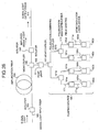
- Fig. 26 is a block diagram of one example of a conventional Raman amplifier used in a WDM communication system.
- semiconductor laser modules 182a to 182d which include Fabry-Perot type semiconductor light-emitting elements 180a to 180d and fiber gratings 181a to 181 d in corresponding pairs, output to polarization-combining couplers 161 a and 161 b laser beams to constitute the pump light.
- the semiconductor laser modules 182a and 182b output laser beams of the same wavelength.
- the polarization-combining coupler 161 a combines the laser beams, aligned to have different polarization directions.
- the semiconductor laser modules 182c and 182d output laser beams of the same wavelength.
- the polarization-combining coupler 161b combines the laser beams, aligned to have different polarization directions.
- the polarization-combining couplers 161a and 161 b output the polarization-combined laser beams to the WDM coupler 162.
- the laser beams output from the polarization-combining couplers 161a and 161 b have different wavelengths.
- the WDM coupler 162 couples the laser beams output from the polarization-combining couplers 161a and 161b and outputs the coupled laser beam to an amplification fiber 164 as the pump light through an isolator 160 and a WDM coupler 165.
- the signal light to be amplified is input from a signal light input fiber 169 through an isolator 163 to the amplification fiber 164 to which the pump light is input, where the signal light is coupled with the pump light and Raman amplified.
- the process of manufacturing the optical fiber amplifier will be complicated if the laser beams to be polarization-combined are emitted from stripe structures of different semiconductor elements.
- the size of the optical fiber amplifier also needs to be scaled up. Therefore, in order to solve these problems, a method of fabricating a Raman amplifier by using a semiconductor laser device that has two stripes on a single semiconductor substrate is proposed in Japanese Patent Laid-Open Publication No. 2001-402819. In this instance, it is possible to simplify the manufacturing process and to downsize the semiconductor laser device itself since a plurality of stripes is fabricated on the single substrate.
- the two stripes arranged in parallel to each other are disposed extremely close to each other, with a spacing not more than 100 ⁇ m, or about 40 ⁇ m for instance, with a resonator formed by the common cleavage surface.
- the two stripes have almost the same physical structure and, hence, their resonator lengths are almost identical.
- the temperatures of their active layers are almost the same. Consequently, oscillation longitudinal mode wavelengths of the emitted laser beams, as well as a spacing of a plurality of oscillation longitudinal modes, are likely to coincide between the two stripes.
- the oscillation longitudinal modes of the laser beams emitted from the different stripes overlaps, it is not possible any longer to reduce the DOP by polarization-combining the laser beams.
- This problem though more conspicuous in a W stripe laser device, may occur even if the two stripes are disposed on different substrates.
- the phenomenon may be considered to occur because the overlapping of the oscillation longitudinal modes of the two laser beams that are polarization-combined may reduce the fluctuation of phase difference of the two oscillation longitudinal modes being combined, especially when the line width of the oscillation longitudinal modes are narrow, giving rise to a particular polarization state corresponding to the phase difference of the two modes in the combined laser beam.
- the semiconductor laser device includes a first stripe structure which has at least a first active layer deposited on a part of the area of a semiconductor substrate, and a first electrode disposed on the first active layer, and which emits a first laser beam, a second stripe structure which has at least a second active layer deposited on the rest of the area of the semiconductor substrate, and a second electrode disposed on the second active layer, and which emits a second laser beam, and a non-current-injection area which is formed on a part of the area of the upper surface of the first stripe structure and into which no injection current flows.
- a semiconductor laser device having a W stripe structure has a non-current-injection area on the upper surface of one of the stripes. Therefore, the lengths of resonators on the two stripes are different effectively. Consequently, the oscillation longitudinal mode spacing and the oscillation longitudinal mode wavelength of the first laser beam and the second laser beam differ. As a result, the oscillation longitudinal modes of the two laser beams do not overlap and hence it is possible to reduce the DOP.
- the semiconductor laser device further includes a second non-current-injection area formed on a part of the upper surface of the second stripe structure and into which no current flows, the second non-current-injection area having a surface area different from the surface area of the first non-injection area.
- the surface area of the non-current-injection area in the first stripe and the second stripe differ. Consequently, the oscillation longitudinal mode wavelengths of the laser beams from the two stripe structures are made to differ.
- the semiconductor laser device includes the non-current-injection area formed by disposing the first electrode only on the area excluding the non-current-injection area on the upper surface of the first stripe structure.
- the non-current-injection area is formed as an area where the electrode is not disposed. Consequently, it is possible to easily form a non-current-injection area.
- the semiconductor laser device further includes a first spacer layer disposed between the first active layer and the first electrode, a second spacer layer disposed between the second active layer and the second electrode, a first diffraction grating which is disposed on a part of the area of the first spacer layer, and which selects a first laser beam including a plurality of oscillation longitudinal modes having a specific center wavelength, and a second diffraction grating which is disposed on a part of the area of the second spacer layer, and which selects a second laser beam including a plurality of oscillation longitudinal modes having a specific center wavelength.
- the present invention by providing diffraction gratings, it is possible to select laser beams having a plurality of oscillation longitudinal modes. Further, by providing a non-current-injection area, it is possible to realize laser oscillations in the first stripe structure and the second stripe structure that occur in oscillation longitudinal modes of different wavelengths.
- the semiconductor laser device includes the first diffraction grating that is disposed in an area below the non-current-injection area.
- the first diffraction grating is disposed in an area below the non-current-injection area. Therefore, there is no flow of current and a resultant variation of refractive index in the first diffraction grating. Consequently, it is possible to reduce the variation of the center wavelength selected by the first diffraction grating.
- the semiconductor laser device includes a first stripe structure which has at least a first active layer deposited on a part of the area of a semiconductor substrate, and a first electrode disposed on the first active layer, and which emits a first laser beam, and a second stripe structure which has at least a second active layer deposited on the rest of the area of the semiconductor substrate, and a second electrode disposed on the second active layer, and which emits a second laser beam.
- the thermal conduction efficiency between the first active layer and the first electrode differs from the thermal conduction efficiency between the second active layer and the second electrode.
- the temperature in the first active layer and the temperature in the second active layer are made to differ by varying the thermal conduction efficiency. Consequently, the oscillation longitudinal mode wavelength of the first laser beam and the oscillation longitudinal mode wavelength of the second laser beam can be made to differ, so as to suppress the overlapping of the two oscillation longitudinal modes. As a result, it is possible to reduce the DOP.
- the semiconductor laser device further includes a first diffraction grating disposed in the vicinity of the first active layer such that the first laser beam has a plurality of oscillation longitudinal modes with a specific center wavelength, and a second diffraction grating disposed in the vicinity of the second active layer such that the second laser beam has a plurality of oscillation longitudinal modes with a specific center wavelength.
- a first laser beam and a second laser beam each having a specific center wavelength and including a plurality of oscillation longitudinal modes can be emitted. Further, by varying thermal conduction efficiency in the first stripe structure and the second stripe structure, laser oscillations of different oscillation longitudinal mode wavelengths can be realized.
- the semiconductor laser device has the width of the first stripe structure in the lateral direction and the width of the second stripe structure in the lateral direction that differ from each other.
- the thermal conduction efficiency of the first stripe and the thermal conduction efficiency of the second stripe can be made to differ from each other by making the widths of the stripe structures in the lateral direction different.
- the semiconductor laser device has the distance between the first active layer and the first electrode and the distance between the second active layer and the second electrode that differ from each other.
- the thermal conduction efficiency of the first stripe different from the thermal conduction efficiency of the second stripe by varying the distance between the active layer and the electrode in the first stripe and the second stripe.
- the semiconductor laser device further includes a first clad layer deposited between the first active layer and the first electrode, and a second clad layer deposited between the second active layer and the second electrode, wherein the thickness of the first clad layer and the thickness of the second clad layer are different from each other.
- the distance between the active layer and the electrode is made to differ in the first stripe and the second stripe by varying the film thickness of the clad layer. Consequently, it is possible to make the thermal conduction efficiency of the first stripe different from the thermal conduction efficiency of the second stripe.
- the semiconductor laser device includes a first stripe structure which has a first active layer deposited on a part of the area of a semiconductor substrate and a first diffraction grating disposed in the vicinity of the first active layer, and which emits a first laser beam having multiple oscillation longitudinal modes with a specific center wavelength, and a second stripe structure which has a second active layer deposited on the rest of the area of the semiconductor substrate and a second diffraction grating disposed in the vicinity of the second active layer, and which emits a second laser beam having multiple oscillation longitudinal modes with a specific center wavelength.
- the center wavelength selected by the first diffraction grating and the center wavelength selected by the second diffraction grating are different from each other.
- the structures of the diffraction grating of the first stripe and the second stripe differ. Consequently, it is possible to make the center wavelength selected by the first stripe different from the center wavelength selected by the second stripe.
- the semiconductor laser device includes a period of the first diffraction grating and a period of the second diffraction grating that differ from each other such that the center wavelength selected by the first diffraction grating and the center wavelength selected by the second diffraction grating are different from each other.
- the period of the diffraction grating in each stripe is made to differ. Consequently, it is possible to vary the center wavelength selected by each stripe.
- the semiconductor laser device includes a first stripe structure which has a first active layer deposited on a part of the area of a semiconductor substrate and a first diffraction grating disposed in the vicinity of the first active layer that selects a first laser beam having multiple oscillation longitudinal modes and a specific center wavelength, and a second stripe structure which has a second active layer deposited on the rest of the area of the semiconductor substrate and a second diffraction grating disposed in the vicinity of the second active layer that selects a second laser beam having multiple oscillation longitudinal modes and a specific center wavelength.
- a difference between the center wavelength of the first laser beam and the center wavelength of the second laser beam is not less than 0.5 times a wavelength spacing between the adjoining oscillation longitudinal modes of the first laser beam or the second laser beam.
- the difference between the center wavelength of the first laser beam and the center wavelength of the second laser beam is not less than 0.5 times the wavelength spacing between the adjoining oscillation longitudinal modes of the first laser beam or the second laser beam. Consequently, it is possible to reduce the DOP of the combined light, irrespective of whether the oscillation longitudinal modes of the laser beams emitted from the two stripes overlap or not.
- the semiconductor laser device has the difference between the center wavelength of the first laser beam and the center wavelength of the second laser beam which is not less than 1.5 times the wavelength spacing between the adjoining oscillation longitudinal modes of the first laser beam or the second laser beam.
- the difference between the center wavelength of the first laser beam and the center wavelength of the second laser beam is not less than 1.5 times the wavelength spacing between the adjoining oscillation longitudinal modes of the first laser beam or the second laser beam. Consequently, it is possible to reduce the DOP of the combined light to 10% or lower, irrespective of whether the oscillation longitudinal modes of the laser beams emitted from the two stripes overlap or not.
- the semiconductor laser device has the difference between the center wavelength of the first laser beam and the center wavelength of the second laser beam which is not less than 5 times the wavelength spacing between the adjoining oscillation longitudinal modes of the first laser beam or the second laser beam.
- the difference between the center wavelength of the first laser beam and the center wavelength of the second laser beam is not less than 5 times the wavelength spacing between the adjoining oscillation longitudinal modes of the first laser beam or the second laser beam. Consequently, it is possible to reduce the DOP of the combined light to 5% or lower, irrespective of whether the oscillation longitudinal modes of the laser beams emitted from the two stripes overlap or not.
- the semiconductor laser device includes a first stripe structure which has a first active layer deposited on a part of the area of a semiconductor substrate and a first diffraction gratingthat selects a first laser beam having multiple oscillation longitudinal modes and a specific center wavelength, and a second stripe structure which has a second active layer deposited on the rest of the area of the semiconductor substrate and a second diffraction grating that selects a second laser beam having multiple oscillation longitudinal modes and a specific center wavelength.
- a difference between the peak wavelength of the first laser beam and the peak wavelength of the second laser beam is not less than 0.01 nm.
- the difference between the peak wavelength of the first laser beam and the peak wavelength of the second laser beam is not less than 0.01 nm. Consequently, the overlapping of two oscillation longitudinal modes is suppressed. As a result, it is possible to reduce the DOP.
- the semiconductor laser device includes a first stripe structure which has a first active layer deposited on a part of the area of a semiconductor substrate and a first diffraction gratingthat selects a first laser beam having multiple oscillation longitudinal modes and a specific center wavelength, and a second stripe structure which has a second active layer deposited on the rest of the area of the semiconductor substrate and a second diffraction grating that selects a second laser beam having multiple oscillation longitudinal modes and a specific center wavelength.
- a difference between the wavelength of all the oscillation longitudinal modes having intensity not more than 3 dB below a peak power in the first laser beam and the wavelength of all the oscillation longitudinal modes having intensity not more than 3 dB below a peak power in the second laser beam, is not less than 0.01 nm.
- the difference between two oscillation longitudinal modes above a specific power is not less than 0.01 nm. Consequently, the overlapping of two oscillation longitudinal modes is suppressed. As a result, it is possible to reduce the DOP.
- the semiconductor laser device has the difference not less than 0.1 nm.
- the difference is not less than 0.1 nm. Consequently, the overlapping of two oscillation longitudinal modes is suppressed. As a result, it is possible to reduce the DOP.
- the semiconductor laser device has an oscillation wavelength spectrum formed by the plurality of oscillation longitudinal modes that belong to the first laser beam and an oscillation wavelength spectrum formed by the plurality of oscillation longitudinal modes that belong to the second laser beam, which do not cross each other in a range in which the intensity difference with respect to the peak power is not more than 3 dB.
- portions above a specific intensity in the two oscillation wavelength spectrums do not cross each other. Consequently, even if oscillation longitudinal modes overlap, the intensity of these oscillation longitudinal modes are small. As a result, it is possible to reduce the DOP.
- the semiconductor laser device has the center wavelength of the second laser beam lower than the center wavelength of the first laser beam, and a difference between a frequency corresponding to the minimum wavelength of the oscillation longitudinal modes having intensity not more than 10 dB below the peak power in the first laser beam and a frequency corresponding to the maximum wavelength of the oscillation longitudinal modes having intensity not more than 10 dB below the peak power in the second laser beam, which is greater than an electrical frequency band width of an optical transmission system being used.
- the oscillation longitudinal modes of the first laser beam and the oscillation longitudinal modes of the second laser beam above a specific power have a frequency difference not less than a specific value. Consequently, it is possible to suppress the beat noise, or even if the beat noise does occur, it is possible to cause it to occur outside the frequency band of the optical transmission system being used.
- the semiconductor laser module includes a semiconductor laser device according to the present invention, a first lens on which the first laser beam and the second laser beam emitted from the semiconductor laser device are incident, a polarization rotating unit into which only any one of the first laser beam and the second laser beam that have passed through the first lens is incident, and which rotates the polarization plane of the incident laser beam by a predetermined angle, a polarization-combining unit having a first port on which the first laser beam from the first lens or the polarization rotating unit is incident, a second port on which the second laser beam from the polarization rotating unit or the first lens is incident, and a third port from which the first laser beam incident from the first port and the second laser beam incident from the second portare combined and emerge, and an optical fiber which receives the laser beams emerging from the third port of the polarization-combining unit, and which transmits the received laser beams to the outside.
- the first laser beam and the second laser beam that are emitted from the semiconductor laser device are polarization-combined, and the polarization-combined beam is output to the optical fiber. Therefore, it is possible to emit a laser beam with a reduced DOP.
- the semiconductor module according to still another aspect of the present invention has the first lens that is a single lens which separates the first laser beam and the second laser beam so as to widen a distance between the two laser beams.
- the single lens is used to separate the first laser beam and the second laser beam so as to widen the distance between the two laser beams, and the two laser beams are first separated and then polarization-combined. Consequently, even if the stripes are close to each other, it is possible to easily design and assemble the parts for polarization-combining the two laser beams emitted from these stripes.
- the optical fiber amplifier includes a pump light source which uses a semiconductor laser device or a semiconductor laser module according to the present invention, a coupler that couples a signal light with a pump light, and an amplification optical fiber which amplifies a light by a Raman amplification.
- the above semiconductor laser device or semiconductor laser module is used. Therefore, it is possible to provide an optical fiber amplifier that is pumped by laser beams with reduced DOP.
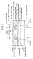
- Fig. 1 is a front cross-section of a semiconductor laser device according to a first embodiment of the present invention
- Fig. 2 is a cross-section of the semiconductor laser device shown in Fig. 1 cut along the line A-A
- Fig. 3 is a cross-section of the semiconductor laser device shown in Fig. 1 cut along the line B-B
- Fig. 4 is a front cross-section of a modification of the semiconductor laser device according to the first embodiment
- Fig. 5 is a front cross-section of a semiconductor laser device according to a second embodiment of the present invention
- Fig. 6(a) and Fig. 6(b) are cross-sections of the semiconductor laser device shown in Fig. 5 cut along the line A-A and the line B-B, respectively;
- Fig. 6(a) and Fig. 6(b) are cross-sections of the semiconductor laser device shown in Fig. 5 cut along the line A-A and the line B-B, respectively;
- FIG. 7 shows an oscillation wavelength spectrum and oscillation longitudinal modes of one center wavelength in the semiconductor laser device shown in Fig. 5;
- Fig. 8 illustrates a relation between optical intensity of the oscillation longitudinal mode and a threshold value of an stimulated Brillouin scattering in the cases. of single longitudinal mode oscillation and multi-longitudinal mode oscillation, respectively;
- Fig. 9 is a cross-section of a semiconductor laser device according to a third embodiment of the present invention;
- Fig. 10 is a cross-section of a semiconductor laser device according to a modification of the third embodiment;
- Fig. 11(a) and Fig. 11(b) are side cross-sections of a semiconductor laser device according to a fourth embodiment of the present invention;
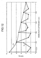
- FIG. 12 is a graph showing the correlation between a center wavelength difference and a degree of polarization
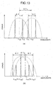
- Fig. 13(a) and Fig. 13(b) illustrate a relation between a center wavelength of a diffraction grating and a wavelength of an oscillation longitudinal mode of peak intensity of each laser beam in the semiconductor laser device according to the fourth embodiment
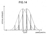
- Fig. 14 illustrates a status of overlapping of oscillation longitudinal modes for a case of a wavelength difference of 0.2 nm
- Fig. 15 is oscillation spectrum waveforms of two laser beams in a condition where a wavelength difference is set in such a way that an oscillation longitudinal mode of one laser beam is interleaved between two adjacent oscillation longitudinal modes of the other laser beam
- Fig. 13(a) and Fig. 13(b) illustrate a relation between a center wavelength of a diffraction grating and a wavelength of an oscillation longitudinal mode of peak intensity of each laser beam in the semiconductor laser device according to the fourth embodiment
- Fig. 14 illustrates
- FIG. 16 illustrates a status of two oscillation wavelength spectrums not intersecting each other above a specific intensity
- Fig. 17 is a block diagram of a semiconductor laser beam source
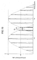
- Fig. 18 illustrates oscillation spectral waveforms of two laser beams by which the beat noise frequency range becomes out of the frequency range of an optical transmission system
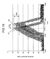
- Fig. 19 is a graph of oscillation spectral waveforms of two laser beams having different center wavelengths by 1.5 nm
- Fig. 20 is a graph of RIN measured for a polarization-combined light that has transmitted over a long distance
- Fig. 21 is a side cross-section of a semiconductor laser module according to a fifth embodiment of the present invention
- Fig. 21 is a side cross-section of a semiconductor laser module according to a fifth embodiment of the present invention
- Fig. 22 is a schematic explanatory diagram of the semiconductor laser module according to the fifth embodiment
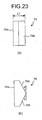
- Fig. 23(b) and Fig. 23(b) are a side view and a plan view of a prism, respectively
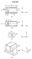
- Fig. 24(a), Fig. 24(b), and Fig. 24(c) are a plan cross-section, a side cross-section, and a front view of a holder supporting a prism a half-wave plate and a polarization-combining unit, respectively
- Fig.24(d) is a perspective view of the holder supported by a second supporting member
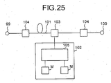
- Fig. 25 is a block diagram of an optical fiber amplifier according to a sixth embodiment of the present invention
- Fig. 26 is a block diagram of a conventional optical fiber amplifier
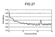
- Fig. 27 is a graph illustrating a beat noise generated after propagating a long distance according to a conventional technology.
- FIG. 1 is a front cross-section showing a structure of the semiconductor laser device according to the first embodiment of the present invention.
- Fig. 2 is a cross-section of the semiconductor laser device shown in Fig. 1 cut along the line A-A.
- Fig. 3 is a cross-section of the semiconductor laser device shown in Fig. 1 cut along the line B-B.
- the semiconductor laser device has an n-InP clad layer 2 deposited on an n-InP substrate 1.
- a lower GRIN-SCH (Graded Index-Separate Confinement Heterostructure) layer 3a, an active layer 4a, and an upper GRIN-SCH layer 5a are deposited in a mesa shape. These will be collectively called a stripe 15.
- a lower GRIN-SCH layer 3b, an active layer 4b, and an upper GRIN-SCH layer 5b are deposited in a mesa shape. These will be collectively called a stripe 16.
- the stripe 15 and the stripe 16 are separated by a space between them.
- a p-InP blocking layer 9 and an n-InP blocking layer 10 are deposited sequentially on the n-InP clad layer 2 to form a structure such that an injection current flows only into the stripe 15 and the stripe 16.
- a p-InP clad layer 6 is deposited on the upper GRIN-SCH layers 5a and 5b and the n-InP blocking layer 10.
- a p-InGaAsP contact layer 7 and p-side electrode are sequentially deposited on the p-InP clad layer 6.
- An n-side electrode 11 is disposed on the lower surface of the n-InP substrate 1.
- the n-InP clad layer 2 achieves a function of a buffer layer as well as that of a clad layer.
- the semiconductor laser device according to the first embodiment has a double-hetero structure formed by sandwiching the stripe 15 and the stripe 16 with the n-InP clad layer 2 and p-InP clad layer 6, which enables effective confinement of carriers and high light-emission efficiency.
- the active layers 4a and 4b employ, for example, a compressive strain quantum well structure of a lattice mismatching ratio within a range of 0.5 % to 1.5% to the n-InP substrate 1.
- This structure is advantageous from the viewpoint of a high output. If the strain quantum well structure employs a strain compensation structure having a barrier layer formed with a tensile stain opposite to a strain of the well layer, it is possible to equivalently meet a lattice matching condition. Therefore, it is not necessary to provide an upper limit to a lattice mismatching ratio of the well layer. In this case, a compressive quantum well having five wells and a lattice mismatching ratio of 1% is used.
- the stripe 15 consists of a deposited structure of the lower GRIN-SCH layer 3a, the active layer 4a, and the upper GRIN-SCH layer 5a, thereby forming what is called a GRIN-SCH-MQW (Graded Index-Separate Confinement Heterostructure-Multiple Quantum Well) active layer. Based on this structure, it becomes possible to confine carriers more effectively. Therefore, combined with the double-hetero structure, the semiconductor laser device according to the first embodiment has high light emission efficiency. This similarly applies to the stripe 16.as well.
- Fig. 2 shows the structure of the cross-section of the semiconductor laser device cut along the line A-A.
- a low reflection film 13 is disposed on the entire surface of an emission-side end surface (the right-side end surface in Fig. 2), and a high reflection film 12 is disposed on the entire surface of a reflection-side end surface (the left-side end surface in Fig. 2).
- a p-side electrode 8a is disposed on the entire surface of the p-InGaAsP contact layer 7.
- the high reflection film 12 has a light reflectivity of 80% or above, preferably 98% or above.
- the low reflection film consists of a film structure of a low reflectivity, having a light reflectivity of not more than 5%, preferably about 1%.
- Fig. 3 shows the structure of the semiconductor laser device appearing in the cross-section cut along the line B-B.
- the low reflection film 13 is disposed on the emission-side end surface, and the high reflection film 12 is disposed on the reflection-side end surface, in a similar manner to the structure appearing in the A-A cross-section.
- a p-side electrode 8b is disposed on the surface of the p-InGaAsP contact layer 7 excluding a portion of this surface.
- Each stripe shown in Fig. 2 and Fig. 3 has a resonator length of 800 ⁇ m to 3200 ⁇ m.
- a current is injected from the p-side electrode 8, and a light-emission recombination of carriers occurs in the stripe 15 and the stripe 16.
- a light generated in this process is amplified in a resonator formed by the high reflection film 12 and the low reflection film 13through a stimulated emission, and a laser beam is emitted from the low reflection film 13.
- effective resonator lengths are different for the stripe 15 and the stripe 16. That is, since the p-side electrode 8a of the stripe 15 is disposed on the whole surface of the p-InGaAsP contact layer 7 as shown in Fig. 2, while the p-side electrode 8b of the stripe 16 is disposed only o'n a part of and not on the entire surface of the p-InGaAsP contact layer 7 as shown in Fig. 3, the current injected to carry out a laser oscillation flows only to the portion below the p-side electrode 8b in the stripe 16, and not to the portion below the region where p-side electrode 8b is not present.
- a refractive index of a semiconductor single-crystal varies based on a current that flows inside the single-crystal. Therefore, in the semiconductor laser device according to the first embodiment, the refractive index of the semiconductor single-crystal that constitutes the stripe 15 and the stripe 16 varies because of the existence of the injection current at the time of laser oscillation.
- the injection current flows into the whole of the stripe 15, but does not flow into a portion of the stripe 16. Therefore, the refractive index varies over the whole length of the semiconductor single crystal that constitutes the stripe 15. However, in the stripe 16, there occurs no variation in the refractive index in the portion where no current flows. Consequently, the optical path length, taking into account the refractive index, are different between the stripe 15 and the stripe 16, although their physical resonator lengths are the same.
- the oscillation longitudinal mode wavelength and their spacing of the semiconductor laser device are determined based on an effective resonator length that takes into account the refractive index, the oscillation longitudinal mode wavelength and the oscillation longitudinal mode spacing of laser beams that are oscillated from the stripe 15 and the stripe 16 of the semiconductor laser device according to the first embodiment are different correspondingly to the difference in the optical path lengths.
- a semiconductor laser device having a conventional W stripe structure is structured in such a way that the physical resonator lengths of the stripes are equal, and the injection current flows uniformly into each stripe. Therefore, the oscillation longitudinal mode wavelengths of the laser beams emitted from the stripes are completely identical.
- the oscillation longitudinal mode wavelength of the laser beam emitted from the stripe 15 and the oscillation longitudinal mode wavelength of the laser beam emitted from the stripe 16 are different from each other, though slightly.
- the semiconductor laser device according to the first embodiment unlike in the semiconductor laser device having a conventional W stripe structure, the overlapping of the two oscillation longitudinal modes is suppressedand the DOP can be reduced.
- the stripe 15 and the stripe 16 have the same structure except for p-side electrodes 8a and 8b. Therefore, the semiconductor laser device according to the first embodiment is easy to manufacture. That is, the semiconductor laser device according to the first embodiment of the present invention can be manufactured by the manufacturing method which differs from that of the conventional semiconductor laser device only in that the electrode is not formed in the area where the non-current-injection area 14 is to be provided, with the other processes in the method being completely identical to the conventional ones. Therefore, it is another advantage of the semiconductor laser device according to the present invention that it can be easily manufactured using a conventional manufacturing apparatus. Note that a contact layer in the non-current-injection area 14 should preferably be eliminated in order to ensure the prevention of diffusion of current to this area.
- Fig. 4 is a front cross-section showing a structure of a modification of the semiconductor laser device according to the first embodiment.
- a separation groove 21 is formed between the stripe 15 and the stripe 16, which reaches to a depth of the n-InP contact layer 2 from the p-side electrode 8.
- the stripe 15 and the stripe 16 can be electrically separated by covering the surface of the separation groove 21 with an insulation film 20.
- a semiconductor laser device that has a wavelength selecting means like DFB or DBR.
- Such type of semiconductor laser device if used as a pump light source for the Raman amplifier, would make it possible to obtain an optical output of stabilized oscillation wavelength even without a fiber grating for wavelength selection.
- a non-current-injection area 14 is provided only in the stripe 16.
- the non-current-injection area 14 may be provided in both the stripe 15 and the stripe 16. In this case, by providing different surface areas of the non-current-injection area in the two stripes, the amount of injected current to the stripe 15 and the stripe 16 can be made different from each other, whereby it is possible to obtain laser beams of different wavelengths.
- a semiconductor laser device according to a second embodiment of the present invention will be described below.
- parts that are assigned the same reference numerals or symbols as those in the first embodiment have similar structures and functions to those of the corresponding parts of the first embodiment. Therefore, their explanation will be omitted.
- Fig. 5 is a front cross-section showing a structure of a semiconductor laser device according to the second embodiment.
- a stripe 18a has a p-InP spacer layer 17a deposited on an upper GRIN-SCH layer 5a
- a stripe 18b has a p-InP spacer layer 17b deposited on an upper GRIN-SCH layer 5b.
- Fig. 6(a) is a cross-section of the semiconductor laser device shown in Fig. 5 cut along the line A-A.
- the semiconductor laser device according to the second embodiment has a structure in which a diffraction grating 23a is disposed in apart of the area within the p-InP spacer layer 17a.
- Fig. 6(b) is a cross-section of the semiconductor laser device shown in Fig. 5 cut along the line B-B, which shows that a diffraction grating 23b is disposed in a part of the area within the p-InP spacer layer 17b.
- These diffraction grating 23a and 23b are made of p-InGaAsP.
- Each diffraction grating has a film thickness of 20 nm, and a length of 50 ⁇ m in a laser emission direction (i.e. the lateral direction in Fig. 6(a) and Fig. 6(b)). Further, each diffraction grating has a single period of 220 nm.
- the diffraction gratings 23a and 23b being constituted as such, they can select a laser beam that has a plurality of oscillation longitudinal modes having a center wavelength of 1480 nm.
- the stripe 18a has a p-side electrode 8a disposed over the whole surface of a p-InGaAsP contact layer 7.
- the stripe 18b has a p-side electrode 8b disposed on a portion on the p-InGaAsP contact layer 7, thereby forming a non-current-injection area 14 on the area on which the p-side electrode 8b is not disposed.
- a low reflection film is made to have a light reflectivity of not more than 1%, preferably not more than 0.01% so that the effect of reflection of Fabry Perot modes at the emission end surface is suppressed.
- the semiconductor laser device in the second embodiment is assumed to be used as an pump light source for the Raman amplifier, and has an oscillation wavelength ⁇ o of 1100 nm to 1550 nm, and a resonator length Lfrom 800 ⁇ m to 3200 ⁇ m inclusive.
- the mode spacing ⁇ of the longitudinal modes is about 0.39 nm for the case of resonator length L being 800 ⁇ m, and about 0.1 nm for the case of resonator length L being 3200 ⁇ m.
- the larger the resonator length the shorter the mode spacing ⁇ of the longitudinal mode may become, and the more difficult it may become for a selection condition to be met that allows the laser beam to oscillate in a single longitudinal mode.
- the diffraction grating 23a selects a longitudinal mode based on a Bragg wavelength thereof.
- the selection wavelength characteristic of the diffraction grating 23a is expressed as an oscillation wavelength spectrum 23 shown in Fig. 7.
- a plurality of oscillation longitudinal modes is made to exist in a wavelength selection characteristic expressed in terms of a half width ⁇ h of the oscillation wavelength spectrum 30 of the semiconductor laser device having the diffraction grating.
- the conventional DFB (Distributed-Feedback) semiconductor laser device has been difficult to oscillate in single longitudinal mode if the resonator length L is set to not less than 800 ⁇ m. Therefore, a semiconductor laser device having such a resonator length L has not been used.
- the semiconductor laser device of the second embodiment positively adopts a resonator length not less than 800 ⁇ m so that it emits a laser beam including a plurality of oscillation longitudinal modes within the half-width ⁇ h of the oscillation wavelength spectrum.
- a resonator length not less than 800 ⁇ m so that it emits a laser beam including a plurality of oscillation longitudinal modes within the half-width ⁇ h of the oscillation wavelength spectrum.
- Fig. 7 there are three oscillation longitudinal modes 31 to 33 included in the half width ⁇ h of the oscillation wavelength spectrum.
- the use of such laser beam having a plurality of oscillation longitudinal modes makes it possible to obtain a high laser output overall, with the intensity of individual oscillation longitudinal mode being suppressed as compared with the case of a laser beam oscillating in single longitudinal mode.
- the semiconductor laser device according to the second embodiment has an oscillation spectrum shown in Fig. 8(b), where a high laser output is achieved overall with reduced intensity of individual longitudinal mode.
- Fig. 8(a) shows an oscillation spectrum of a semiconductor laser device that oscillates in a single longitudinal mode to obtain the same laser output, where the longitudinal mode has a larger intensity.
- the semiconductor laser device when used as a pump light source for the Raman amplifier, it is preferable to increase a pumping optical output power in order to increase a Raman gain.
- the oscillation longitudinal mode is intense, noise is generated to a greater extent through stimulated Brillouin scattering. Since the stimulated Brillouin scattering occurs when the oscillation longitudinal mode intensity exceeds the threshold Pth, Brillouin scattering can be suppressed by including a plurality of oscillation longitudinal modes within the laser beam, while keeping overall laser output, and thereby suppressing the intensity of each oscillation longitudinal mode below the threshold Pth of stimulated Brillouin scattering, as shown in Fig. 8(b). In this way, a high Raman gain can be obtained.
- a plurality of oscillation longitudinal modes is included in the half-width ⁇ h of the oscillation wavelength spectrum 30.
- the half-width ⁇ h of the oscillation wavelength spectrum 30 should be not more than 3 nm, or more preferably, not more than 2 nm.
- the wavelength interval (mode spacing) ⁇ between the oscillation longitudinal modes 31 to 33 is 0.1 nm or higher. This is because in case of using the semiconductor laser device as a pumping light source for the Raman amplifier, the stimulated Brillouin scattering is more likely to occur if the mode spacing ⁇ is not more than 0.1 nm.
- the resonator length L is preferably not more than 3200 ⁇ m.
- the conventional semiconductor laser device since the conventional semiconductor laser device has been used in a semiconductor laser module with a fiber grating, the resonance between the fiber grating and the light reflection surface has caused an increase in relative intensity noise (RIN) and hampered a stable Raman amplification.
- the semiconductor laser device shown in the second embodiment is not equipped with a fiber grating so that a laser beam emitted from the low reflection film 13 is directly used as an pump light source for the Raman amplifier, it is possible to reduce the relative intensity noise, and consequently, fluctuations in Raman gain. Therefore, it is possible to carry out a stable Raman amplification.
- the semiconductor laser device according to the second embodiment has another advantage which arises from combination with the structures of the p-side electrodes 8a and 8b.
- the semiconductor laser device according to the second embodiment since the semiconductor laser device according to the second embodiment has non-current injection areas 14 like those in the first embodiment, the wavelength of each oscillation longitudinal mode of the laser beam emitted from the stripe 18a and the wavelength of each oscillation longitudinal mode of the laser beam emitted from the stripe 18b are different from each other. Therefore, it is possible to suppress overlapping of the oscillation longitudinal modes, resulting in sufficient reduction of DOP, when such two laser beams are polarization-combined. It is also possible, similarly to the first embodiment, to simplify the manufacturing process of the semiconductor laser device and to make the device compact, as compared with the case where laser beams from two distinct semiconductor laser devices are polarization-combined.
- the semiconductor laser device according to the third embodiment of the present invention has a plurality of stripe structures on a single semiconductor substrate.
- An oscillation longitudinal mode wavelength of a laser beam emitted by each stripe is made different by varying the width of each stripe in the lateral direction. This is explained in more detail with reference to Fig. 9.
- the semiconductor laser device has a stripe 50a and a stripe 50b on a single n-InP substrate 1.
- the stripe 50a includes a lower GRIN-SCH layer 46a, an active layer 47a, an upper GRIN-SCH layer 48a, and a p-InP spacer layer 49a deposited sequentially.
- the stripe 50b includes a lower GRIN-SCH layer 46b, an active layer 47b, an upper GRIN-SCH layer 48b, and a p-InP spacer layer 49b deposited sequentially.
- the width La of the stripe 50a in lateral direction is greater than the width Lb of the stripe 50b in lateral direction.
- the p-InP spacer layer 49a and 49b each includes, similar to the second embodiment, a diffraction grating that selects a laser beam having a specific center wavelength and a plurality of oscillation longitudinal modes. Parts that are identical or similar to those in the first embodiment or second embodiment are assigned identical or similar reference numerals or symbols and have identical or similar functions.
- the laser beam emitted by each stripe is caused to have a different oscillation longitudinal mode wavelength by varying the width of each stripe in lateral direction.
- the reason for the difference in the oscillation longitudinal mode wavelength of the laser beam emitted by each stripe is explained.
- heat produced in the active layer due to a light non-emission recombination current etc. acts to raise the temperature around the active layer, giving an adverse effect on the characteristic of the emitted laser beam.
- the semiconductor laser device is fixed junction down on a heat sink, making the heat sink to come in contact with the upper electrode, thereby dissipating the heat produced.
- the semiconductor laser device according to the third embodiment is fixed junction down as well, with a p-side electrode 8 being in contact with the heat sink. Consequently, the heat produced in the active layer 47a during laser oscillation is released into the heat sink through the upper GRIN-SCH layer 48a, the p-InP spacer layer 49a, and a p-InP clad layer 6. Similarly, the heat produced in the active layer 47b is released into the heat sink through the upper GRIN-SCH layer 48b, the p-InP spacer layer 49b and the p-InP clad layer 6. In this way, the heat produced in the active layers 47a and 47b are released to the outside through the stripes 50a, and 50b, respectively and the area above the stripes 50a and 50b, all of which collectively function as a thermal conduction channel.
- the thermal conduction efficiency in general, proportionally increases with the cross-sectional area of the thermal conduction channel.
- the cross-sectional area of the stripes 50a and 50b differ because of the difference in their widths La and Lb. Therefore, the respective thermal conduction efficiencies of the stripe 50a and the stripe 50b are different. Consequently, during laser oscillation, the temperature in the vicinity of the active layer 47a and the temperature in the vicinity of the active layer 47b are different.
- the refractive index of the semiconductor single-crystals depends on the temperature. And since the wavelength of each oscillation longitudinal mode and the oscillation longitudinal mode spacing are dependent on the optical path length determined by taking into account the refractive index, they are different between the laser beam emitted from the stripe 50a and the laser beam emitted from the stripe 50b. When such two laser beams are polarization-combined, the overlapping of the two oscillation longitudinal modes is suppressed. Therefore, the DOP of the combined beam can be sufficiently reduced.
- an electrical resistance to the injected current also varies due to the difference in the lateral width. That is, since the electrical resistance is inversely proportional to the cross-sectional area, the stripes 50a and 50b, which have different widths, have different value of electrical resistance from each other. Therefore, the electric current flowing into the active layer 47a and the electric current flowing into the active layer 47b are different, which causes not only the wavelength of each oscillation longitudinal mode to be different between the two stripes based on the similar reason to the first embodiment, but also the amount of heat produced in the active layers 47a and 47b to be different from each other, leading to different temperatures of the active layers 47a and 47b and different wavelengths of oscillation longitudinal modes between the two stripes.
- each stripe has a diffraction grating for wavelength selection in the third embodiment, it is also possible to use Fabry-Perot resonators for wavelength selection, as in the first embodiment.
- the semiconductor laser device is fixed p-side down on the heat sink.
- the semiconductor laser device may be fixed on the heat sink so that an n-side electrode 11 comes in contact with the heat sink.
- the heat produced in the active layers 47a and 47b is released to the heat sink through stripes 50a and 50b, respectively, and the area below the stripes 50a and 50b, which collectively act as a thermal conduction channel. Therefore, by having different widths La and Lb, the thermal conduction efficiencies can be different between the stripes 50a and 50b.
- the oscillation longitudinal mode wavelengths of the laser beams emitted by the stripes 50a and 50b are different from each other. Consequently, the DOP can be reduced.
- Fig. 10 is a cross-section showing a structure of the modification of the semiconductor laser device. As shown in Fig. 10, in semiconductor laser device according to the modification, the thermal conduction efficiency is made to differ by varying a thickness of a p-InP clad layer 51.
- the thermal conduction efficiency is made to differ by varying the cross-sectional areas of the thermal conduction channels.
- the thermal conduction efficiency can be made to differ also by varying the lengths of the thermal conduction channels, in case of equal cross sectional areas.
- the variation in the length of the thermal conduction channel can be achieved not only by varying the thickness of the p-InP clad layer 51 but also by varying those of the p-InP spacer layers 49a and 49b.
- each stripe is formed a diffraction grating that selects a plurality of oscillation longitudinal modes and the structure of diffraction gratings is different from one another so that each diffraction grating selects a different center wavelength.
- the fourth embodiment is explained below with reference to Fig. 11.
- Fig. 11(a) and Fig. 11(b) are a side cross-sections that show the structure of the semiconductor laser device according to the fourth embodiment (the front cross-section is the same as Fig. 5 and hence is omitted).
- Fig. 11(a) illustrates a stripe 52a that includes a diffraction grating 53a.
- Fig. 11 (b) illustrates a stripe 52b that includes a diffraction grating 53b.
- the diffraction gratings 53a and 53b have different periods so that the center wavelength selected by the diffraction grating 53a is different from the center wavelength selected by the diffraction grating 53b.
- the inventors of the present invention measured the relation between a wavelength difference ⁇ p, which is a difference of a peak wavelength (a wavelength of the oscillation longitudinal mode of maximum intensity amongst plural oscillation longitudinal modes that constitute an oscillation wavelength spectrum) of a laser beam emitted from each stripe, and the DOP.
- orthogonally polarization-combined laser beams each beam emitted by each one of two semiconductor laser devices having a single stripe, were measured for DOP with changing wavelength difference ⁇ p.
- the two semiconductor laser devices used for the purpose of measurement each had a diffraction grating in the vicinity of its active layer and emitted a laser beam having a plurality of oscillation longitudinal modes arranged with a spacing of 0.2 nm therebetween.
- each of the semiconductor laser device bearing a single stripe structure was mounted on a separate temperature-adjusting module so as to vary the temperature of the active layer and thereby to vary the peak wavelength.
- the tendency of DOP of the combined light versus changing wavelength difference ⁇ p represented by the result of measurement obtained for two separate semiconductor laser devices bearing a single stripe structure, applies equally to a semiconductor laser device bearing a W stripe structure whose peak wavelengths of the laser beams emitted from the two stripes are different from each other.
- Fig. 12 is a graph showing the result of the measurement.
- the horizontal axis indicates the wavelength difference ⁇ p and the vertical axis indicates DOP.
- the curve I 1 shows a variation of the DOP over a short cycle
- the curve I 2 shows a variation of the DOP over a long cycle.
- the DOP fluctuates cyclically for every 0.2 nm of the wavelength difference ⁇ p.
- the DOP tends to decrease as the wavelength difference ⁇ p increases over the long cycle, as shown by curve I 2 .
- the DOP can be suppressed to 10% or lower, and if the wavelength difference ⁇ p is not less than 0.8 nm, the DOP can be suppressed to 5% or lower.
- the DOP can be reduced by increasing the wavelength difference ⁇ p.
- the reason for the cyclical behavior of DOP is as follows.
- the two semiconductor laser devices used in the present measurement emit laser beams each having a plurality of oscillation longitudinal modes with the longitudinal mode spacing ( ⁇ : Expression 1) of 0.2nm, based on their respective diffraction gratings. If the wavelength difference ⁇ p of such two laser beams is 0.2 nm, then the relation between the two laser beams are shown in Fig. 14, where the oscillation longitudinal modes of the two laser beams overlap, even though the peak wavelengths of their oscillation spectrums are different from each other. In such a situation, the DOP does not reduce sufficiently. However, as the wavelength difference ⁇ p increases, the intensity difference of the overlapping oscillation longitudinal modes increases and the number of oscillation longitudinal modes decreases. Therefore, the DOP tends to decrease over a long cycle.
- the wavelengths of the oscillation longitudinal modes of the two laser beams are slightly shifted with respect to each other (by 0.01 nm to 0.2 nm), whereby the DOP can be suppressed.
- the oscillation longitudinal modes of the two laser beams appear as shown in Fig. 15, where the oscillation longitudinal mode of one laser beam is interspersed between two adjacent oscillation longitudinal modes of the other laser beam.
- the center wavelength selected by the diffraction gratings 53a and 53b are made as different as possible whereby the DOP of the combined light is reduced irrespective of whether the oscillation longitudinal modes of the two stripes overlap or not, unlike in the first to third embodiments in which the DOP of the combined light is reduced by preventing the overlapping of the oscillation longitudinal modes, which is attained through changing the electrode structure or layer structure of the semiconductor laser device,.
- Fig. 13(a) illustrates an instance in which the oscillation longitudinal mode of maximum intensity (with peak wavelength ⁇ p1 ) of the first laser beam is on the short wavelength side with respect to the center wavelength ⁇ G1 of the diffraction grating 53a formed in the first stripe structure 52a, and the oscillation longitudinal mode of maximum intensity (with peak wavelength ⁇ p2 ) of the second laser beam is on the long wavelength side with respect to the center wavelength ⁇ G2 of the diffraction grating 53b formed in the second stripe structure 52b.
- a DOP can be reduced at least to 5% or less if the wavelength difference ⁇ p is not less than four times the oscillation longitudinal mode spacing ⁇ (that is, not less than 0.8 nm).
- the DOP can be reduced to either 10% or 5%respectively, irrespective of whether the oscillation longitudinal modes overlap or not.
- the difference ⁇ G between the center wavelengths can be reduced when the peak wavelength is more or less equal.to the center wavelength, that is, when ⁇ p1 ⁇ G1 and ⁇ p2 ⁇ G2 .
- the wavelength difference ⁇ p is not less than half of the oscillation longitudinal mode spacing ⁇ when : ⁇ G ⁇ ⁇ p ⁇ ⁇ /2
- the DOP reduces to 10% or lower. Even if ⁇ G and ⁇ p are only more or less the same and do not match exactly, the DOP can be reduced to about 10%.
- the DOP of the combined light can be reduced by applying any one of oscillation longitudinal mode spacing ⁇ in expressions (2) through (4).
- Another method for determining the center wavelength of the diffraction grating of each stripe so that the DOP of the combined light can be reduced is to evade overlapping of the oscillation wavelength spectrums 54 and 55 of two laser beams on their portion above a specific power, as shown in Fig. 16.
- the center wavelength difference of the diffraction gratings ⁇ p should be set such that the portion of the oscillation wavelength spectrums 54 and 55 having an intensity difference not more than 3 dB with respect to the maximum intensities of the laser beams do not cross each other.
- the center wavelength difference ⁇ p such that the oscillation wavelength spectrums 54 and 55 do not cross in the range in which the intensity difference with respect to the maximum intensity of the laser beams is not more than 10 dB.
- the DOP of the polarization-combined laser beam can be effectively reduced, by setting the wavelength difference ⁇ p to be 1.5 times, preferably 5 times, the oscillation longitudinal mode spacing ⁇ , or by setting the wavelength difference ⁇ p such that the oscillation wavelength spectrums do not cross in the range in which the intensity ratio to the maximum is not more than a predetermined value, specifically 3 dB, or preferably 10 dB.
- This method of setting the wavelength difference ⁇ p is not limited to the semiconductor laser beam source formed from a semiconductor laser device having a W stripe structure, but is applicable to the semiconductor laser beam source formed from two separate semiconductor laser devices which has a stripe each on two different substrates. In the latter case as well, the DOP of the polarization-combined beams can be effectively reduced by setting the wavelength difference ⁇ p as described above.
- the structures shown in Fig. 17(a) and Fig. 17(b) can be used. As shown in Fig.
- an pump light source with reduced DOP can be fabricated by a semiconductor laser beam source 59a that includes two semiconductor laser devices 58a and 58b each having a single stripe, which have a wavelength difference of ⁇ p in the range described above.
- the laser beams emitted from the two semiconductor laser devices 58a and 58b are orthogonally polarization-combined by a polarization-combining coupler 60.
- laser beams emitted from two single stripe semiconductor laser devices 58a and 58b that form the semiconductor laser beam source 59b can be directed into the polarization-combining coupler (cube beam splitter) 62 in such a way that the two laser beams are orthogonal to each other.
- the laser beam which is emitted from the single stripe semiconductor laser device 58a and collimated by a lens 61 a and the laser beam which is emitted from the single stripe semiconductor laser device 58b, collimated by a lens 61b, and passed through a half-wave plate 61c, are orthogonally polarization-combined by the polarization-combining coupler 62.
- a light with reduced DOP is input into a transmission optical fiber 64.
- the two laser beams can be made to have a wavelength difference described above by appropriately adjusting the temperature of each semiconductor laser device.
- the DOP of the combined light can be reduced by setting the wavelength of the two laser beam between the cyclical peak of the DOP shown in Fig. 12 through a fine-tuning of the wavelength of each laser beam. For instance, according to the trend of the curve I 1 of Fig. 12, the DOP of the combined light can be lowered by making the wavelength difference of the oscillation longitudinal modes of the laser beams emitted from the two semiconductor light sources not less than 0.01 nm, preferably not less than 0.1 nm.
- the above wavelength difference may be made on all the oscillation longitudinal modes.
- the DOP of the combined light can be reduced by making the above-described wavelength difference on the oscillation longitudinal modes of intensity ratio not more than 3 dB, preferably not more than 10 dB, to the peak intensity.
- ⁇ the oscillation longitudinal mode spacing between two adjoining oscillation longitudinal modes
- n a natural number.
- the oscillation longitudinal modes of one laser beam are interspersed between the oscillation longitudinal modes of the other laser beam, as shown in Fig. 15.
- the overlapping of the oscillation longitudinal modes of the two laser beams is prevented. Consequently, the DOP of the orthogonally polarization-combined laser light can be reduced.
- beat noise does occur, at least its adverse effect can be avoided if it can be made to occur outside the transmission band of the optical transmission system in which the semiconductor laser device is used. This is because the beat noise that appears outside the transmission band will not be a cause of signal noise that occurs during Raman amplification.
- the wavelength difference ⁇ p should be set in the following manner.
- the center wavelengths ⁇ p1 and ⁇ p2 should be set such that the frequency difference between the oscillation longitudinal mode 65 belonging to the laser beam emitted from the first stripe of a center wavelength ⁇ p1 , and having maximum wavelength among the plurality of oscillation longitudinal modes of intensity not more than 10 dB below maximum intensity of the emitted laser beam, and the oscillation longitudinal mode 66 belonging to the laser beam emitted from the second stripe of a center wavelength ⁇ p2 (> ⁇ p1 ), and having minimum wavelength among the plurality of oscillation longitudinal modes of intensity not more than 10 dB below maximum intensity of the emitted laser beam, should be greater than the electrical band width of the optical transmission system in which the semiconductor laser device is used. In this way, even if the polarization mixing occurs during long-distance transmission of the laser beam over the optical fiber, the beat noise may occur only in a frequency range outside the transmission band of the transmission
- the diffraction grating of each stripe should be set in such a way that the wavelength difference ⁇ p is not less than a few nm to a few tens of nm (for example, not less than 3 nm). More preferably; the wavelength difference ⁇ p may be not less than 20 nm.
- the laser beam emitted from one stripe may have a center wavelength of 1430 nm, while the laser beam emitted from the other stripe may have a center wavelength of 1450 nm.
- Fig. 19 is a graph showing waveforms of the laser beams emitted by the two stripes when the wavelength difference ⁇ p is set to 1.5 nm.
- the laser beam emitted from the first stripe has a center wavelength of 1447.5 nm, and includes the oscillation longitudinal mode 67 whose wavelength is maximum among those longitudinal modes of intensity not more than10dB below the maximum intensity.
- the laser beam emitted from the second stripe has a center wavelength of 1449 nm, and includes the oscillation longitudinal mode 68 whose wavelength is minimum among those longitudinal modes of intensity not more than 10dB below the maximum intensity.
- Fig. 20 is a graph showing a relative intensity noise in the polarization-combined laser beams after transmitted over a long distance in an optical fiber. It is evident that the peak that appeared around 11 GHz in Fig. 27 is absent in Fig. 20.
- a semiconductor laser module according to the fifth embodiment of the present invention uses the semiconductor laser device according to the first embodiment.
- Fig. 21 is a side cross-section showing a structure of the semiconductor laser module according to the fifth embodiment
- Fig. 22 is an explanatory diagram schematically showing a structure of the semiconductor laser module according to the fifth embodiment.
- the semiconductor laser module according to the fifth embodiment has a package 71 with the inside sealed hermetically, a semiconductor laser device 72 that emits a laser beam, a photodiode 73, a first lens 74, a prism 75, a half-wave plate (a polarization rotating unit) 76, and a polarization beam combiner (PBC) 77, all of which are provided inside the package 71, and an optical fiber 78.
- the semiconductor laser device 72 has a stripe 79 and a stripe 80 that are formed in parallel on the same plane in a longitudinal direction with a distance between the stripes.
- the stripe 79 and the stripe 80 emit a first laser beam K1 and a second laser beam K2 from their respective end surfaces.
- K1 and K2 show tracks of centers of the beams emitted from the stripe 79 and the stripe 80 respectively. The beams propagate with a certain spread around the centers, as indicated by broken lines in Fig. 22.
- the distance between the stripe 79 and the stripe 80 is about 40 ⁇ m, for example.
- the semiconductor laser device 72 is fixed to the upper surface of a chip carrier 81.
- the semiconductor laser device 72 may be fixed to the upper surface of a heat sink (not shown), which further is fixed to the upper surface of the chip carrier 81.
- the photodiode 73 receives a laser beam for monitoring, emitted from a rear end surface 72b (the left side end surface in Fig. 21) of the semiconductor laser device 72.
- the photodiode 73 is fixed to a photodiode carrier 82.
- the first lens 74 receives the first laser beam K1 and the second laser beam K2 emitted from an end surface 72a of a front end surface (the right side end surface in Fig. 21) of the semiconductor laser device 72.
- the first lens 74 widens the distance between the first laser beam K1 and the second laser beam K2 and focuses the laser beams at different focal points (F1 and F2).
- the first lens 74 is held by a first lens holding member 83.
- the first lens 74 is positioned such that the optical axis of the first laser beam K1 emitted from the stripe 79 and the optical axis of the second laser beam K2 emitted from the stripe 80 are substantially symmetric with respect to the center axis of the first lens 74.
- both of the first laser beam K1 and the second laser beam K2 pass through areas near the center axis of the first lens 74, where the aberrations are small. Therefore, there occurs no disturbance in the wave surfaces of the laser beams, and the optical coupling efficiency to the optical fiber 78 is high.
- the first lens 74 may be an aspheric lensof small spherical aberration, which can suppress the effect of spherical aberration and can augment thereby a coupling efficiency to the optical fiber 78.
- the prism 75 is disposed between the first lens 74 and the polarization beam combiner 77 such that the first laser beam K1 and second laser beam K2 are incident thereon and emitted therefrom along their mutually parallel optical axes.
- the prism 75 is made of an optical glass like BK7 (boro-silicated crown glass) or the like.
- BK7 boro-silicated crown glass
- the optical axes of the first and second laser beams K1 and K2, that propagate in non-parallel from the first lens 74, are made parallel based on the refraction of the prism 75. Therefore, it is easy to prepare the polarization beam combiner 77 that is disposed at the back of this prism 75. At the same time, it is easy to downsize the polarization beam combiner 77, and the semiconductor laser module thereby.
- Fig. 23(a) A is a side view showing a structure of the prism 75
- Fig. 23(b) is a plan view of this prism.
- the prism 75 is about 1.0 mm in total length L1, and has a flat input surface 75a and an output surface 75b inclined at a specific angle ⁇ ( ⁇ lies in a range 3.2° ⁇ 0.1°).
- the half-wave plate 76 receives only the first laser beam K1, and rotates its polarization plane by 90°.
- the polarization beam combiner 77 has a first port 77a on which the first laser beam K1 is incident, a second port 77b on which the second laser beam K2 is incident, and a third port 77c from which the first laser beam K1 incident on the first port 77a and the second laser beam K2 incident on the second port 77b are combined and emerges.
- the polarization beam combiner 77 is a birefringent element that transmits the first laser beam K1 to the third port 77c as an ordinary ray, and transmits the second laser beam K2 to the third port 77c as an extraordinary ray. If the polarization beam combiner 77 is made of a birefringent element, TiO 2 (rutile), for example, may be used to get a large separation width between the laser beams, because of its large birefringence.
- TiO 2 rutile
- Fig. 24(a) is a plan cross-section showing the holder member 84 supporting the prism 75, the half-wave plate 76, and the polarization beam combiner 77
- Fig. 24(b) is a side cross-section of this holder
- Fig. 24(c) is a front view of this holder.
- the holder member 84 is prepared using a material to which YAG laser welding can be applied (for example, SUS403, 304, and the like).
- the holder member 84 has a total length L2 of about 7.0 mm, and is substantially cylindrical in shape.
- the holder member 84 has an accommodating section 84a, where the prism 75, the half-wave plate 76, and the polarization beam combiner 77 are fixed.
- the upper part and lower part of the holder member 84 are flat.
- the holder member 84 is fixed between two upright walls of a second supporting member 89b having substantially a U-shaped cross-section.
- the holder member 84 can be disposed between the upright walls; being rotated around a center axis C1.
- the position of the holder member 84a can be easily adjusted along X, Y, and Z axes and around the center axis C1 such that the first laser beam K1 incident on the first port 77a and the second laser beam K2 incident on the second port 77b of the polarization beam combiner 77 emerges from the third port 77c.
- the optical fiber 78 receives the laser beams emerging from the third port 77c of the polarization beam combiner 77, and transmits the laser beams to the outside.
- a second lens 86 that optically couples the combined laser beams emerging from the third port 77c of the polarization beam combiner 77 to the optical fiber 78 is disposed between the polarization beam combiner 77 and the optical fiber 78.
- the first lens 74 is positioned such that the first laser beam K1 and the second laser beam K2 are focused at the focal points (F1 and F2) between the first lens 74 and the second lens 86.
- the chip carrier 81 to which the semiconductor laser device 72 is fixed, and the photodiode carrier 82 to which the photodiode 73 is fixed, are fixed by soldering onto a first base 87 having substantially an L-shaped cross section.
- the first base 87 is made of a CuW alloy or the like in order to be efficient in radiation of the heat generated by the semiconductor laser device 72.
- the first lens holding member 83 to which the first lens 74 is fixed, and the holder member 84 to which the prism 55, the half-wave plate 76, and the polarization beam combiner 77 are fixed, are fixed onto a second base 88 by YAG laser welding via a first supporting member 89a and a second supporting member 89b, respectively.
- the second base 88 is prepared preferably using a stainless steel or the like of excellent weldability. Further, the second base 88 is fixed onto a flat section 87a of the first base 87 by brazing.
- a cooling unit 90 including a Peltier element is provided on the lower portion of the first base 87.
- a thermistor 90a provided on the chip carrier 81 detects a rise in temperature due the heat generated by the semiconductor laser device 72.
- the cooling unit 90 controls the temperature detected by the thermistor 90a to a constant temperature. Based on this, it is possible to increase and stabilize the laser beams output from the semiconductor laser device 72.
- An intermediate member 71d is fixed to the end surface of the flange section 71a.
- a second lens holding member 91 holding the second lens 86 for focusing the laser beam is fixed to the inside of the intermediate member 71d by YAG welding..
- a ferrule 93 holding the optical fiber 78 is fixed to the end of the second lens holding member through a metal slide ring 92 by YAG welding.
- the operation of the semiconductor laser module according to the fifth embodiment will be explained below.
- the distance (D) between the first laser beam K1 and the second laser beam K2 at the incidence on the prism 55 is about 480 ⁇ m.
- the first laser beam K1 and the second laser beam K2 are made parallel to each other by the prism 75 and emerge from the prism 75 (the distance between the beams at this point is about 500 ⁇ m). Thereafter, the first laser beam K1 is incident on the half-wave plate 76, where the polarization plane is rotated by 90°, and then is incident on the first port 77a of the polarization beam combiner 77, while the second laser beam K2 is incident on the second port 77b of the polarization beam combiner 77.
- the polarization beam combiner 77 combines the first laser beam K1 incident on the first port 77a and the second laser beam K2 incident on the second port 77b, and the combined beams emerge from the third port 77c.
- the second lens 86 focuses the laser beams emerging from the polarization beam combiner 77.
- the focused beams are incident on the end surface of the optical fiber 78 supported by the ferrule 93, and are transmitted to the outside.
- the photodiode 73 receives, for monitoring, the laser beam emitted from the rear end surface 72b of the semiconductor laser device 72.
- the optical output etc. is adjusted by controlling the operating current to the semiconductor laser device 72, based on the intensity of received light at the photodiode 73.
- the semiconductor laser device 72 emits the first laser beam K1 and the second laser beam K2, which are polarization-combined through the half-wave plate 76 which rotates the polarization plane of the first laser beam K1 by 90°, and the polarization beam combiner 77 which polarization-combines the first laser beam K1 and the second laser beam K2. Therefore, the laser beams of high output and with small degree of polarization can be obtained from the optical fiber 78, and hence, it is possible to apply the above semiconductor laser module as for use an pump light source for the energy-doped optical fiber amplifier that requires a high output, and the Raman amplifier that additionally requires a low polarization dependency and wavelength stability.
- the semiconductor laser module is structured using the semiconductor laser device according to the first embodiment.
- the structure is not limited to this.
- a semiconductor laser device having a wavelength selecting unit like the DFB and the DBR, or the semiconductor laser device according to the second to fourth embodiments may be used. Rather, these semiconductor laser devices are preferable since they eliminate the need of fiber gratings when being used in optical fiber amplifiers.
- the optical fiber amplifier according to the sixth embodiment of the present invention carries out an optical amplification based on a Raman amplification.
- Fig. 25 is a block diagram showing a configuration of the optical fiber amplifier according to the sixth embodiment.
- the optical fiber amplifier according to the sixth embodiment has an input section 99 to which an signal light is input, an output section 100 from which the signal light is output, an optical fiber (an amplification fiber) 101 that transmits the signal light between the input section 99 and the output section 100, a pump light generating section 102 that generates an pump light, and a WDM coupler 103 that combines the pump light generated by the pump light generating section 102 and the signal light transmitted in the optical fiber (an amplification fiber) 101.
- An optical isolator 104 is provided between the input section 99 and the WDM coupler 103, and between the output section 100 and the WDM coupler 103, respectively, allowing only the signal light in the direction from the input section 99 to the output section 100.
- the pump light generating section 102 includes two of semiconductor laser module M according to the fifth embodiment, emitting laser beams of different wavelength bands, and a WDM coupler 105 that combines the laser beams emitted from the semiconductor laser modules M.
- the pump lights emitted from the semiconductor laser modules M are combined by the WDM coupler 105, and constitute an output beam of the pump light generating section 102.
- the pump light generated by the pump light generating section 102 are coupled to the optical fiber 101 by the WDM coupler 103.
- the signal light input from the input section 99 is combined with pump light in the optical fiber 101, whereby the signal lights are Raman-amplified.
- the amplified signal lights pass through the WDM coupler 103, and are output from the output section 100.
- optical fiber amplifier according to the sixth embodiment it is possible to lower the DOP by using the semiconductor laser module according to the fifth embodiment, whereby, a stable and high-gain optical amplification can be carried out irrespective of the polarization direction of the signal light.
- the optical fiber amplifier can be manufactured easily and can be downsized as well.
- a semiconductor laser device having a W stripe structure has a non-current-injection area on the upper surface of one of the stripes. Therefore, the lengths of resonators on the two stripes are substantially different. Consequently, the oscillation longitudinal mode wavelengths and their spacing are different in the first laser beam and the second laser beam. As a result, the oscillation longitudinal modes of the two laser beams do not overlap which leads to reduction of the DOP.
- the surface areas of the non-current-injection areas 'in the first stripe and the second stripe differ. Consequently, the oscillation longitudinal mode wavelengths of the laser beams from the two stripe structures are different, leading to reduction of the DOP.
- the non-current-injection area is formed as an area where the electrode is not disposed. Consequently, it is possible to form a non-current-injection area easily.
- the partially provided diffraction gratings enable to select laser beams having a specific center wavelength and including a plurality of oscillation longitudinal modes.
- the first stripe structure and the second stripe structure are provided to oscillate in different longitudinal modes.
- the first diffraction grating is disposed in an area below the non-current-injection area. Therefore, there is no flow of current and a resultant variation of refractive index in the first diffraction grating, which reduces the variation of the center wavelength selected by the first diffraction grating.
- the temperature in the first active layer and the temperature in the second active layer are made to differ by varying the thermal conduction efficiency. Consequently, the oscillation longitudinal mode wavelength of the first laser beam and the oscillation longitudinal mode wavelength of the second laser beam can be different so that the overlapping of the two oscillation longitudinal modes are suppressed, whereby the DOP can be reduced.
- diffraction gratings provided enable to emit a first laser beam and a second laser beam having a specific center wavelength and including a plurality of oscillation longitudinal modes.
- thermal conduction efficiency in the first stripe structure and the second stripe structure it is possible make the stripes to oscillate at different longitudinal mode wavelengths.
- the width of the stripe structure in the lateral direction is made to differ in the first stripe and the second stripe so that the thermal conduction efficiencies are different in the first stripe and the second stripe.
- the distance between the active layer and the electrode is made to differ in the first stripe and the second stripe so that the thermal conduction efficiencies are different in the first stripe and the second stripe.
- the distance between the active layer and the electrode is made to differ in the first stripe and the second stripe by varying the film thickness of the clad layerso that the thermal conduction efficiencies are different in the first stripe and the second stripe.
- the structures of the diffraction grating of the first stripe and the second stripe differso that the center wavelengths selected by the first stripe and the center wavelength selected by the second stripe are different.
- the period of the diffraction grating in each stripe is made to differ so that the center wavelength selected by each stripe is different.
- the difference between the center wavelength of the first laser beam and the center wavelength of the second laser beam is not less than 0.5 times the wavelength spacing between the adjoining oscillation longitudinal modes of the first laser beam and the second laser beam. Consequently, the DOP of the combined light can be reduced, irrespective of whether the oscillation longitudinal modes of the laser beams emitted from the two stripes overlap or not.
- the difference between the center wavelength of the first laser beam and the center wavelength of the second laser beam is not less than 1.5 times the wavelength spacing between the adjoining oscillation longitudinal modes of the first laser beam and the second laser beam. This has the effect of being able to reduce the DOP of the combined light to 10% or lower, irrespective of whether the oscillation longitudinal modes of the laser beams emitted from the two stripes overlap or not.
- the difference between the center wavelength of the first laser beam and the center wavelength of the second laser beam is not less than 5 times the wavelength spacing between the adjoining oscillation longitudinal modes of the first laser beam and the second laser beam. This has the effect of being able to reduce the DOP of the combined light to 5% or lower, irrespective of whether the oscillation longitudinal modes of the laser beams emitted from the two stripes overlap or not.
- the difference between the peak wavelength of the first laser beam and the peak wavelength of the second laser beam is not less than 0.01 nm. Consequently, the overlapping of two oscillation longitudinal modes is suppressed, whereby the DOP can be reduced.
- the difference between two oscillation longitudinal modes above a specific intensity is not less than 0.01 nm. Consequently, the overlapping of two oscillation longitudinal modes is suppressed, whereby the DOP can be reduced.
- the difference is not less than 0.1 nm. Consequently, the overlapping of two oscillation longitudinal modes is suppressed, whereby the DOP can be reduced.
- the two oscillation wavelength spectrums do not cross each other on the portions above a specific intensity. Consequently, even if oscillation longitudinal modes overlap, the intensity of these oscillation longitudinal modes are small. As a result, it is possible to reduce the DOP.
- the oscillation longitudinal modes above a specific intensity of the first laser beam and of the second laser beam have a frequency difference not less than a specific value. It has the effect of being able to suppress the beat noise, or even if the beat noise does occur, it can be outside the frequency band of the optical transmission system to which the semiconductor laser device is used.
- the first laser beam and the second laser beam emitted from the semiconductor laser device are polarization-combined, and the polarization-combined beam is output to the optical fiber. This has the effect of being able to emit a laser beam of a reduced DOP.
- a single lens is used to separate the first laser beam and the second laser beam so as to widen the distance between the two laser beams. Since the two laser beams are first separated and then polarization-combined, , it is easy to design and assemble the parts required for polarization-combining the two laser beams emitted from these stripes, even if the stripes are close to each other.
- the semiconductor laser device, the semiconductor laser module, and the optical fiber amplifier using the semiconductor laser module according to the present invention are suitable for a pumping source for Raman amplification, and suitable for realizing stable and high-gain amplification to be used in an optical transmission system.
Landscapes
- Physics & Mathematics (AREA)
- Optics & Photonics (AREA)
- General Physics & Mathematics (AREA)
- Engineering & Computer Science (AREA)
- Condensed Matter Physics & Semiconductors (AREA)
- Electromagnetism (AREA)
- Nanotechnology (AREA)
- Chemical & Material Sciences (AREA)
- Biophysics (AREA)
- Crystallography & Structural Chemistry (AREA)
- Life Sciences & Earth Sciences (AREA)
- Semiconductor Lasers (AREA)
- Optical Modulation, Optical Deflection, Nonlinear Optics, Optical Demodulation, Optical Logic Elements (AREA)
Abstract
A semiconductor laser device with two active-layer stripe structures has an n-InP substrate (1), an n-InP clad layer (2), a lower GRIN-SCH layer (3b), an active layer (4b), an upper GRIN-SCH layer (5b), a p-InP clad layer (6), and a p-InGaAsP contact layer (7) laminated in this order, in a side cross section including one of the stripe structure. A high-reflection film (12) is disposed on a reflection-side end surface, and a low-reflection film (13) is disposed on an emission-side end surface. A p-side electrode (8b) is disposed on only a part of the upper surface of the p-InGaAsP contact layer (7) so that a current non-injection area (14) is formed on the rest of the area. <IMAGE>
Description
The present invention relates to a semiconductor laser device
having a two-stripe structure, a semiconductor laser module, and an
optical fiber amplifier using the semiconductor laser module, and more
particularly, to a semiconductor laser device, a semiconductor laser
module, and an optical fiber amplifier using the semiconductor laser
module that has low degree of polarization, produces little beat noise
over a long distance, and exhibit a high power output.
In an optical fiber amplifier based on Raman amplification, it is
possible to realize a high-gain optical fiber amplifier by using a high
power pumping source employing a plurality of semiconductor laser
devices. Since the Raman amplification of a signal light takes place
when the polarization of the signal light and the polarization of a pump
light are in correct matching, it is necessary to reduce the effect of
polarization mismatching between the signal light and the pump light.
To achieve this, degree of polarization (DOP) is reduced by eliminating
the polarization of the pump light (i.e., depolarization of the pump light).
Fig. 26 is a block diagram of one example of a conventional
Raman amplifier used in a WDM communication system. In Fig. 26,
semiconductor laser modules 182a to 182d which include Fabry-Perot
type semiconductor light-emitting elements 180a to 180d and fiber
gratings 181a to 181 d in corresponding pairs, output to
polarization-combining couplers 161 a and 161 b laser beams to
constitute the pump light. The semiconductor laser modules 182a and
182b output laser beams of the same wavelength. However, the
polarization-combining coupler 161 a combines the laser beams, aligned
to have different polarization directions. Similarly, the semiconductor
laser modules 182c and 182d output laser beams of the same
wavelength. However, the polarization-combining coupler 161b
combines the laser beams, aligned to have different polarization
directions. The polarization-combining couplers 161a and 161 b output
the polarization-combined laser beams to the WDM coupler 162. The
laser beams output from the polarization-combining couplers 161a and
161 b have different wavelengths.
The WDM coupler 162 couples the laser beams output from the
polarization-combining couplers 161a and 161b and outputs the
coupled laser beam to an amplification fiber 164 as the pump light
through an isolator 160 and a WDM coupler 165. The signal light to be
amplified is input from a signal light input fiber 169 through an isolator
163 to the amplification fiber 164 to which the pump light is input, where
the signal light is coupled with the pump light and Raman amplified.
The process of manufacturing the optical fiber amplifier will be
complicated if the laser beams to be polarization-combined are emitted
from stripe structures of different semiconductor elements. The size of
the optical fiber amplifier also needs to be scaled up. Therefore, in
order to solve these problems, a method of fabricating a Raman
amplifier by using a semiconductor laser device that has two stripes on
a single semiconductor substrate is proposed in Japanese Patent
Laid-Open Publication No. 2001-402819. In this instance, it is possible
to simplify the manufacturing process and to downsize the
semiconductor laser device itself since a plurality of stripes is fabricated
on the single substrate.
However, in the semiconductor laser device that has two stripes
(hereinafter "W stripe laser device") as disclosed in the above Japanese
Patent Laid-Open Publication, the two stripes arranged in parallel to
each other are disposed extremely close to each other, with a spacing
not more than 100 µm, or about 40 µm for instance, with a resonator
formed by the common cleavage surface. The two stripes have almost
the same physical structure and, hence, their resonator lengths are
almost identical. Besides, due to proximity of the two stripes, the
temperatures of their active layers are almost the same. Consequently,
oscillation longitudinal mode wavelengths of the emitted laser beams,
as well as a spacing of a plurality of oscillation longitudinal modes, are
likely to coincide between the two stripes. If the oscillation longitudinal
modes of the laser beams emitted from the different stripes overlaps, it
is not possible any longer to reduce the DOP by polarization-combining
the laser beams. This problem, though more conspicuous in a W
stripe laser device, may occur even if the two stripes are disposed on
different substrates. The phenomenon may be considered to occur
because the overlapping of the oscillation longitudinal modes of the two
laser beams that are polarization-combined may reduce the fluctuation
of phase difference of the two oscillation longitudinal modes being
combined, especially when the line width of the oscillation longitudinal
modes are narrow, giving rise to a particular polarization state
corresponding to the phase difference of the two modes in the
combined laser beam.
Another problem arises due to overlapping of oscillation
longitudinal modes of the laser beams that are polarization-combined.
Normally, immediately after polarization-combining, the polarization
components of the laser beams emitted from the two stripes do not
interfere with each other. However, when RIN (relative intensity noise)
for a laser beam propagated over a long distance is measured, a peak
corresponding to a beat noise is observed in the.vicinity of 11 GHz, as
shown in Fig.27, as a result of a mixing between the orthogonal
polarization components during the long-distance transmission over the
optical fiber. Since the Raman amplification in particular is a nonlinear
process that takes place in an extremely short timescale, a noise that
would develop as shown in Fig.27 due to the beat noise when using the
W stripe laser device as the pump light source, would be translated into
the signal noise that would hamper the signal transmission.
Therefore, it is an object of the present invention to realize a
semiconductor laser device and a semiconductor laser module which
are suitable for an pump light source such as a Raman amplifier, and in
which the degree of polarization is minimal and the beat noise, owing to
long-distance transmission, does not occur, and an optical fiber
amplifier using the semiconductor laser module, which enables a stable
high-gain amplification independently of the polarization direction of the
signal light.
The semiconductor laser device according to one aspect of the
present invention includes a first stripe structure which has at least a
first active layer deposited on a part of the area of a semiconductor
substrate, and a first electrode disposed on the first active layer, and
which emits a first laser beam, a second stripe structure which has at
least a second active layer deposited on the rest of the area of the
semiconductor substrate, and a second electrode disposed on the
second active layer, and which emits a second laser beam, and a
non-current-injection area which is formed on a part of the area of the
upper surface of the first stripe structure and into which no injection
current flows.
According to the present invention, a semiconductor laser
device having a W stripe structure has a non-current-injection area on
the upper surface of one of the stripes. Therefore, the lengths of
resonators on the two stripes are different effectively. Consequently,
the oscillation longitudinal mode spacing and the oscillation longitudinal
mode wavelength of the first laser beam and the second laser beam
differ. As a result, the oscillation longitudinal modes of the two laser
beams do not overlap and hence it is possible to reduce the DOP.
The semiconductor laser device according to another aspect of
the present invention further includes a second non-current-injection
area formed on a part of the upper surface of the second stripe
structure and into which no current flows, the second
non-current-injection area having a surface area different from the
surface area of the first non-injection area.
According to the present invention, the surface area of the
non-current-injection area in the first stripe and the second stripe differ.
Consequently, the oscillation longitudinal mode wavelengths of the
laser beams from the two stripe structures are made to differ.
The semiconductor laser device according to still another aspect
of the present invention includes the non-current-injection area formed
by disposing the first electrode only on the area excluding the
non-current-injection area on the upper surface of the first stripe
structure.
According to the present invention, the non-current-injection
area is formed as an area where the electrode is not disposed.
Consequently, it is possible to easily form a non-current-injection area.
The semiconductor laser device according to still another aspect
of the present invention further includes a first spacer layer disposed
between the first active layer and the first electrode, a second spacer
layer disposed between the second active layer and the second
electrode, a first diffraction grating which is disposed on a part of the
area of the first spacer layer, and which selects a first laser beam
including a plurality of oscillation longitudinal modes having a specific
center wavelength, and a second diffraction grating which is disposed
on a part of the area of the second spacer layer, and which selects a
second laser beam including a plurality of oscillation longitudinal modes
having a specific center wavelength.
According to the present invention, by providing diffraction
gratings, it is possible to select laser beams having a plurality of
oscillation longitudinal modes. Further, by providing a
non-current-injection area, it is possible to realize laser oscillations in
the first stripe structure and the second stripe structure that occur in
oscillation longitudinal modes of different wavelengths.
The semiconductor laser device according to still another aspect
of the present invention includes the first diffraction grating that is
disposed in an area below the non-current-injection area.
According to the present invention, the first diffraction grating is
disposed in an area below the non-current-injection area. Therefore,
there is no flow of current and a resultant variation of refractive index in
the first diffraction grating. Consequently, it is possible to reduce the
variation of the center wavelength selected by the first diffraction
grating.
The semiconductor laser device according to still another aspect
of the present invention includes a first stripe structure which has at
least a first active layer deposited on a part of the area of a
semiconductor substrate, and a first electrode disposed on the first
active layer, and which emits a first laser beam, and a second stripe
structure which has at least a second active layer deposited on the rest
of the area of the semiconductor substrate, and a second electrode
disposed on the second active layer, and which emits a second laser
beam. The thermal conduction efficiency between the first active layer
and the first electrode differs from the thermal conduction efficiency
between the second active layer and the second electrode.
According to the present invention, the temperature in the first
active layer and the temperature in the second active layer are made to
differ by varying the thermal conduction efficiency. Consequently, the
oscillation longitudinal mode wavelength of the first laser beam and the
oscillation longitudinal mode wavelength of the second laser beam can
be made to differ, so as to suppress the overlapping of the two
oscillation longitudinal modes. As a result, it is possible to reduce the
DOP.
The semiconductor laser device according to still another aspect
of the present invention further includes a first diffraction grating
disposed in the vicinity of the first active layer such that the first laser
beam has a plurality of oscillation longitudinal modes with a specific
center wavelength, and a second diffraction grating disposed in the
vicinity of the second active layer such that the second laser beam has
a plurality of oscillation longitudinal modes with a specific center
wavelength.
According to the present invention, by providing diffraction
gratings, a first laser beam and a second laser beam each having a
specific center wavelength and including a plurality of oscillation
longitudinal modes can be emitted. Further, by varying thermal
conduction efficiency in the first stripe structure and the second stripe
structure, laser oscillations of different oscillation longitudinal mode
wavelengths can be realized.
The semiconductor laser device according to still another aspect
of the present invention has the width of the first stripe structure in the
lateral direction and the width of the second stripe structure in the
lateral direction that differ from each other.
According to the present invention, the thermal conduction
efficiency of the first stripe and the thermal conduction efficiency of the
second stripe can be made to differ from each other by making the
widths of the stripe structures in the lateral direction different.
The semiconductor laser device according to still another aspect
of the present invention has the distance between the first active layer
and the first electrode and the distance between the second active layer
and the second electrode that differ from each other.
According to the present invention, it is possible to make the
thermal conduction efficiency of the first stripe different from the
thermal conduction efficiency of the second stripe by varying the
distance between the active layer and the electrode in the first stripe
and the second stripe.
The semiconductor laser device according to still another aspect
of the present invention further includes a first clad layer deposited
between the first active layer and the first electrode, and a second clad
layer deposited between the second active layer and the second
electrode, wherein the thickness of the first clad layer and the thickness
of the second clad layer are different from each other.
According to the present invention, the distance between the
active layer and the electrode is made to differ in the first stripe and the
second stripe by varying the film thickness of the clad layer.
Consequently, it is possible to make the thermal conduction efficiency
of the first stripe different from the thermal conduction efficiency of the
second stripe.
The semiconductor laser device according to still another aspect
of the present invention includes a first stripe structure which has a first
active layer deposited on a part of the area of a semiconductor
substrate and a first diffraction grating disposed in the vicinity of the
first active layer, and which emits a first laser beam having multiple
oscillation longitudinal modes with a specific center wavelength, and a
second stripe structure which has a second active layer deposited on
the rest of the area of the semiconductor substrate and a second
diffraction grating disposed in the vicinity of the second active layer,
and which emits a second laser beam having multiple oscillation
longitudinal modes with a specific center wavelength. The center
wavelength selected by the first diffraction grating and the center
wavelength selected by the second diffraction grating are different from
each other.
According to the present invention, the structures of the
diffraction grating of the first stripe and the second stripe differ.
Consequently, it is possible to make the center wavelength selected by
the first stripe different from the center wavelength selected by the
second stripe.
The semiconductor laser device according to still another aspect
of the present invention includes a period of the first diffraction grating
and a period of the second diffraction grating that differ from each other
such that the center wavelength selected by the first diffraction grating
and the center wavelength selected by the second diffraction grating
are different from each other.
According to the present invention, the period of the diffraction
grating in each stripe is made to differ. Consequently, it is possible to
vary the center wavelength selected by each stripe.
The semiconductor laser device according to still another aspect
of the present invention includes a first stripe structure which has a first
active layer deposited on a part of the area of a semiconductor
substrate and a first diffraction grating disposed in the vicinity of the
first active layer that selects a first laser beam having multiple
oscillation longitudinal modes and a specific center wavelength, and a
second stripe structure which has a second active layer deposited on
the rest of the area of the semiconductor substrate and a second
diffraction grating disposed in the vicinity of the second active layer that
selects a second laser beam having multiple oscillation longitudinal
modes and a specific center wavelength. A difference between the
center wavelength of the first laser beam and the center wavelength of
the second laser beam is not less than 0.5 times a wavelength spacing
between the adjoining oscillation longitudinal modes of the first laser
beam or the second laser beam.
According to the present invention, the difference between the
center wavelength of the first laser beam and the center wavelength of
the second laser beam is not less than 0.5 times the wavelength
spacing between the adjoining oscillation longitudinal modes of the first
laser beam or the second laser beam. Consequently, it is possible to
reduce the DOP of the combined light, irrespective of whether the
oscillation longitudinal modes of the laser beams emitted from the two
stripes overlap or not.
The semiconductor laser device according to according to still
another aspect of the present invention has the difference between the
center wavelength of the first laser beam and the center wavelength of
the second laser beam which is not less than 1.5 times the wavelength
spacing between the adjoining oscillation longitudinal modes of the first
laser beam or the second laser beam.
According to the present invention, the difference between the
center wavelength of the first laser beam and the center wavelength of
the second laser beam is not less than 1.5 times the wavelength
spacing between the adjoining oscillation longitudinal modes of the first
laser beam or the second laser beam. Consequently, it is possible to
reduce the DOP of the combined light to 10% or lower, irrespective of
whether the oscillation longitudinal modes of the laser beams emitted
from the two stripes overlap or not.
The semiconductor laser device according to still another aspect
of the present invention has the difference between the center
wavelength of the first laser beam and the center wavelength of the
second laser beam which is not less than 5 times the wavelength
spacing between the adjoining oscillation longitudinal modes of the first
laser beam or the second laser beam.
According to the present invention, the difference between the
center wavelength of the first laser beam and the center wavelength of
the second laser beam is not less than 5 times the wavelength spacing
between the adjoining oscillation longitudinal modes of the first laser
beam or the second laser beam. Consequently, it is possible to reduce
the DOP of the combined light to 5% or lower, irrespective of whether
the oscillation longitudinal modes of the laser beams emitted from the
two stripes overlap or not.
The semiconductor laser device according to still another aspect
of the present invention includes a first stripe structure which has a first
active layer deposited on a part of the area of a semiconductor
substrate and a first diffraction gratingthat selects a first laser beam
having multiple oscillation longitudinal modes and a specific center
wavelength, and a second stripe structure which has a second active
layer deposited on the rest of the area of the semiconductor substrate
and a second diffraction grating that selects a second laser beam
having multiple oscillation longitudinal modes and a specific center
wavelength. A difference between the peak wavelength of the first
laser beam and the peak wavelength of the second laser beam is not
less than 0.01 nm.
According to the present invention, the difference between the
peak wavelength of the first laser beam and the peak wavelength of the
second laser beam is not less than 0.01 nm. Consequently, the
overlapping of two oscillation longitudinal modes is suppressed. As a
result, it is possible to reduce the DOP.
The semiconductor laser device according to still another aspect
of the present invention includes a first stripe structure which has a first
active layer deposited on a part of the area of a semiconductor
substrate and a first diffraction gratingthat selects a first laser beam
having multiple oscillation longitudinal modes and a specific center
wavelength, and a second stripe structure which has a second active
layer deposited on the rest of the area of the semiconductor substrate
and a second diffraction grating that selects a second laser beam
having multiple oscillation longitudinal modes and a specific center
wavelength. A difference between the wavelength of all the oscillation
longitudinal modes having intensity not more than 3 dB below a peak
power in the first laser beam and the wavelength of all the oscillation
longitudinal modes having intensity not more than 3 dB below a peak
power in the second laser beam, is not less than 0.01 nm.
According to the present invention, the difference between two
oscillation longitudinal modes above a specific power is not less than
0.01 nm. Consequently, the overlapping of two oscillation longitudinal
modes is suppressed. As a result, it is possible to reduce the DOP.
The semiconductor laser device according to still another aspect
of the present invention has the difference not less than 0.1 nm.
According to the present invention, the difference is not less
than 0.1 nm. Consequently, the overlapping of two oscillation
longitudinal modes is suppressed. As a result, it is possible to reduce
the DOP.
The semiconductor laser device according to still another aspect
of the present invention has an oscillation wavelength spectrum formed
by the plurality of oscillation longitudinal modes that belong to the first
laser beam and an oscillation wavelength spectrum formed by the
plurality of oscillation longitudinal modes that belong to the second
laser beam, which do not cross each other in a range in which the
intensity difference with respect to the peak power is not more than 3
dB.
According to the present invention, portions above a specific
intensity in the two oscillation wavelength spectrums do not cross each
other. Consequently, even if oscillation longitudinal modes overlap,
the intensity of these oscillation longitudinal modes are small. As a
result, it is possible to reduce the DOP.
The semiconductor laser device according to still another aspect
of the present invention has the center wavelength of the second laser
beam lower than the center wavelength of the first laser beam, and a
difference between a frequency corresponding to the minimum
wavelength of the oscillation longitudinal modes having intensity not
more than 10 dB below the peak power in the first laser beam and a
frequency corresponding to the maximum wavelength of the oscillation
longitudinal modes having intensity not more than 10 dB below the peak
power in the second laser beam, which is greater than an electrical
frequency band width of an optical transmission system being used.
According to the present invention, the oscillation longitudinal
modes of the first laser beam and the oscillation longitudinal modes of
the second laser beam above a specific power have a frequency
difference not less than a specific value. Consequently, it is possible
to suppress the beat noise, or even if the beat noise does occur, it is
possible to cause it to occur outside the frequency band of the optical
transmission system being used.
The semiconductor laser module according to still another
aspect ofthe present invention includes a semiconductor laser device
according to the present invention, a first lens on which the first laser
beam and the second laser beam emitted from the semiconductor laser
device are incident, a polarization rotating unit into which only any one
of the first laser beam and the second laser beam that have passed
through the first lens is incident, and which rotates the polarization
plane of the incident laser beam by a predetermined angle, a
polarization-combining unit having a first port on which the first laser
beam from the first lens or the polarization rotating unit is incident, a
second port on which the second laser beam from the polarization
rotating unit or the first lens is incident, and a third port from which the
first laser beam incident from the first port and the second laser beam
incident from the second portare combined and emerge, and an optical
fiber which receives the laser beams emerging from the third port of the
polarization-combining unit, and which transmits the received laser
beams to the outside.
According to the present invention, the first laser beam and the
second laser beam that are emitted from the semiconductor laser
device are polarization-combined, and the polarization-combined beam
is output to the optical fiber. Therefore, it is possible to emit a laser
beam with a reduced DOP.
The semiconductor module according to still another aspect of
the present invention has the first lens that is a single lens which
separates the first laser beam and the second laser beam so as to
widen a distance between the two laser beams.
According to the present invention, the single lens is used to
separate the first laser beam and the second laser beam so as to widen
the distance between the two laser beams, and the two laser beams are
first separated and then polarization-combined. Consequently, even if
the stripes are close to each other, it is possible to easily design and
assemble the parts for polarization-combining the two laser beams
emitted from these stripes.
The optical fiber amplifier according to still another aspect of the
present invention includes a pump light source which uses a
semiconductor laser device or a semiconductor laser module according
to the present invention, a coupler that couples a signal light with a
pump light, and an amplification optical fiber which amplifies a light by a
Raman amplification.
According to the present invention, the above semiconductor
laser device or semiconductor laser module is used. Therefore, it is
possible to provide an optical fiber amplifier that is pumped by laser
beams with reduced DOP.
Fig. 1 is a front cross-section of a semiconductor laser device
according to a first embodiment of the present invention; Fig. 2 is a
cross-section of the semiconductor laser device shown in Fig. 1 cut
along the line A-A; Fig. 3 is a cross-section of the semiconductor laser
device shown in Fig. 1 cut along the line B-B; Fig. 4 is a front
cross-section of a modification of the semiconductor laser device
according to the first embodiment; Fig. 5 is a front cross-section of a
semiconductor laser device according to a second embodiment of the
present invention; Fig. 6(a) and Fig. 6(b) are cross-sections of the
semiconductor laser device shown in Fig. 5 cut along the line A-A and
the line B-B, respectively; Fig. 7 shows an oscillation wavelength
spectrum and oscillation longitudinal modes of one center wavelength in
the semiconductor laser device shown in Fig. 5; Fig. 8 illustrates a
relation between optical intensity of the oscillation longitudinal mode
and a threshold value of an stimulated Brillouin scattering in the cases.
of single longitudinal mode oscillation and multi-longitudinal mode
oscillation, respectively; Fig. 9 is a cross-section of a semiconductor
laser device according to a third embodiment of the present invention;
Fig. 10 is a cross-section of a semiconductor laser device according to
a modification of the third embodiment; Fig. 11(a) and Fig. 11(b) are
side cross-sections of a semiconductor laser device according to a
fourth embodiment of the present invention; Fig. 12 is a graph showing
the correlation between a center wavelength difference and a degree of
polarization; Fig. 13(a) and Fig. 13(b) illustrate a relation between a
center wavelength of a diffraction grating and a wavelength of an
oscillation longitudinal mode of peak intensity of each laser beam in the
semiconductor laser device according to the fourth embodiment; Fig. 14
illustrates a status of overlapping of oscillation longitudinal modes for a
case of a wavelength difference of 0.2 nm; Fig. 15 is oscillation
spectrum waveforms of two laser beams in a condition where a
wavelength difference is set in such a way that an oscillation
longitudinal mode of one laser beam is interleaved between two
adjacent oscillation longitudinal modes of the other laser beam; Fig. 16
illustrates a status of two oscillation wavelength spectrums not
intersecting each other above a specific intensity; Fig. 17 is a block
diagram of a semiconductor laser beam source; Fig. 18 illustrates
oscillation spectral waveforms of two laser beams by which the beat
noise frequency range becomes out of the frequency range of an optical
transmission system; Fig. 19 is a graph of oscillation spectral
waveforms of two laser beams having different center wavelengths by
1.5 nm; Fig. 20 is a graph of RIN measured for a polarization-combined
light that has transmitted over a long distance; Fig. 21 is a side
cross-section of a semiconductor laser module according to a fifth
embodiment of the present invention; Fig. 22 is a schematic explanatory
diagram of the semiconductor laser module according to the fifth
embodiment; Fig. 23(b) and Fig. 23(b) are a side view and a plan view
of a prism, respectively; Fig. 24(a), Fig. 24(b), and Fig. 24(c) are a plan
cross-section, a side cross-section, and a front view of a holder
supporting a prism a half-wave plate and a polarization-combining unit,
respectively, and Fig.24(d) is a perspective view of the holder supported
by a second supporting member; Fig. 25 is a block diagram of an
optical fiber amplifier according to a sixth embodiment of the present
invention; Fig. 26 is a block diagram of a conventional optical fiber
amplifier; and Fig. 27 is a graph illustrating a beat noise generated after
propagating a long distance according to a conventional technology.
Exemplary embodiments of a semiconductor laser device, a
semiconductor laser module, and an optical fiber amplifier using the
semiconductor laser module according to the present invention will be
explained with reference to the accompanying drawings. Identical or
similar parts are assigned identical or similar reference numerals or
symbols. It should be noted that the drawings are schematic, and the
relationship between the thickness and the width of a layer, and ratios
of thickness of layers are different from actual ones. Further, not all
parts in the drawings are drawn to scale.
A semiconductor laser device according to a first embodiment of
the present invention will be described below. Fig. 1 is a front
cross-section showing a structure of the semiconductor laser device
according to the first embodiment of the present invention. Fig. 2 is a
cross-section of the semiconductor laser device shown in Fig. 1 cut
along the line A-A. Fig. 3 is a cross-section of the semiconductor laser
device shown in Fig. 1 cut along the line B-B.
As shown in Fig. 1, the semiconductor laser device according to
the first embodiment has an n-InP clad layer 2 deposited on an n-InP
substrate 1. On the A-A line shown in Fig. 1, a lower GRIN-SCH
(Graded Index-Separate Confinement Heterostructure) layer 3a, an
active layer 4a, and an upper GRIN-SCH layer 5a are deposited in a
mesa shape. These will be collectively called a stripe 15. Similarly,
on the B-B line, a lower GRIN-SCH layer 3b, an active layer 4b, and an
upper GRIN-SCH layer 5b are deposited in a mesa shape. These will
be collectively called a stripe 16. The stripe 15 and the stripe 16 are
separated by a space between them. At the portions excluding the
stripe 15 and the stripe 16, a p-InP blocking layer 9 and an n-InP
blocking layer 10 are deposited sequentially on the n-InP clad layer 2 to
form a structure such that an injection current flows only into the stripe
15 and the stripe 16. Further a p-InP clad layer 6 is deposited on the
upper GRIN-SCH layers 5a and 5b and the n-InP blocking layer 10. A
p-InGaAsP contact layer 7 and p-side electrode are sequentially
deposited on the p-InP clad layer 6. An n-side electrode 11 is
disposed on the lower surface of the n-InP substrate 1.
The n-InP clad layer 2 achieves a function of a buffer layer as
well as that of a clad layer. The semiconductor laser device according
to the first embodiment has a double-hetero structure formed by
sandwiching the stripe 15 and the stripe 16 with the n-InP clad layer 2
and p-InP clad layer 6, which enables effective confinement of carriers
and high light-emission efficiency.
The active layers 4a and 4b employ, for example, a compressive
strain quantum well structure of a lattice mismatching ratio within a
range of 0.5 % to 1.5% to the n-InP substrate 1. This structure is
advantageous from the viewpoint of a high output. If the strain
quantum well structure employs a strain compensation structure having
a barrier layer formed with a tensile stain opposite to a strain of the well
layer, it is possible to equivalently meet a lattice matching condition.
Therefore, it is not necessary to provide an upper limit to a lattice
mismatching ratio of the well layer. In this case, a compressive
quantum well having five wells and a lattice mismatching ratio of 1% is
used.
The stripe 15 consists of a deposited structure of the lower
GRIN-SCH layer 3a, the active layer 4a, and the upper GRIN-SCH layer
5a, thereby forming what is called a GRIN-SCH-MQW (Graded
Index-Separate Confinement Heterostructure-Multiple Quantum Well)
active layer. Based on this structure, it becomes possible to confine
carriers more effectively. Therefore, combined with the double-hetero
structure, the semiconductor laser device according to the first
embodiment has high light emission efficiency. This similarly applies
to the stripe 16.as well.
Fig. 2 shows the structure of the cross-section of the
semiconductor laser device cut along the line A-A. A low reflection
film 13 is disposed on the entire surface of an emission-side end
surface (the right-side end surface in Fig. 2), and a high reflection film
12 is disposed on the entire surface of a reflection-side end surface (the
left-side end surface in Fig. 2). A p-side electrode 8a is disposed on
the entire surface of the p-InGaAsP contact layer 7.
The high reflection film 12 has a light reflectivity of 80% or
above, preferably 98% or above. On the other hand, the low reflection
film consists of a film structure of a low reflectivity, having a light
reflectivity of not more than 5%, preferably about 1%.
Fig. 3 shows the structure of the semiconductor laser device
appearing in the cross-section cut along the line B-B. The low
reflection film 13 is disposed on the emission-side end surface, and the
high reflection film 12 is disposed on the reflection-side end surface, in
a similar manner to the structure appearing in the A-A cross-section.
A p-side electrode 8b is disposed on the surface of the p-InGaAsP
contact layer 7 excluding a portion of this surface. Each stripe shown
in Fig. 2 and Fig. 3 has a resonator length of 800 µm to 3200 µm.
In the semiconductor laser device according to the first
embodiment, a current is injected from the p-side electrode 8, and a
light-emission recombination of carriers occurs in the stripe 15 and the
stripe 16. A light generated in this process is amplified in a resonator
formed by the high reflection film 12 and the low reflection film
13through a stimulated emission, and a laser beam is emitted from the
low reflection film 13.
In the semiconductor laser device according to the first
embodiment, effective resonator lengths are different for the stripe 15
and the stripe 16. That is, since the p-side electrode 8a of the stripe
15 is disposed on the whole surface of the p-InGaAsP contact layer 7
as shown in Fig. 2, while the p-side electrode 8b of the stripe 16 is
disposed only o'n a part of and not on the entire surface of the
p-InGaAsP contact layer 7 as shown in Fig. 3, the current injected to
carry out a laser oscillation flows only to the portion below the p-side
electrode 8b in the stripe 16, and not to the portion below the region
where p-side electrode 8b is not present.
A refractive index of a semiconductor single-crystal varies based
on a current that flows inside the single-crystal. Therefore, in the
semiconductor laser device according to the first embodiment, the
refractive index of the semiconductor single-crystal that constitutes the
stripe 15 and the stripe 16 varies because of the existence of the
injection current at the time of laser oscillation.
In the semiconductor laser device according to the first
embodiment, the injection current flows into the whole of the stripe 15,
but does not flow into a portion of the stripe 16. Therefore, the
refractive index varies over the whole length of the semiconductor
single crystal that constitutes the stripe 15. However, in the stripe 16,
there occurs no variation in the refractive index in the portion where no
current flows. Consequently, the optical path length, taking into
account the refractive index, are different between the stripe 15 and the
stripe 16, although their physical resonator lengths are the same.
Since the oscillation longitudinal mode wavelength and their spacing of
the semiconductor laser device are determined based on an effective
resonator length that takes into account the refractive index, the
oscillation longitudinal mode wavelength and the oscillation longitudinal
mode spacing of laser beams that are oscillated from the stripe 15 and
the stripe 16 of the semiconductor laser device according to the first
embodiment are different correspondingly to the difference in the optical
path lengths.
A semiconductor laser device having a conventional W stripe
structure is structured in such a way that the physical resonator lengths
of the stripes are equal, and the injection current flows uniformly into
each stripe. Therefore, the oscillation longitudinal mode wavelengths
of the laser beams emitted from the stripes are completely identical.
On the other hand, in the semiconductor laser device according to the
first embodiment, the oscillation longitudinal mode wavelength of the
laser beam emitted from the stripe 15 and the oscillation longitudinal
mode wavelength of the laser beam emitted from the stripe 16 are
different from each other, though slightly. Hence, in the semiconductor
laser device according to the first embodiment, unlike in the
semiconductor laser device having a conventional W stripe structure,
the overlapping of the two oscillation longitudinal modes is
suppressedand the DOP can be reduced.
In the semiconductor laser device according to the first
embodiment, the stripe 15 and the stripe 16 have the same structure
except for p-side electrodes 8a and 8b. Therefore, the semiconductor
laser device according to the first embodiment is easy to manufacture.
That is, the semiconductor laser device according to the first
embodiment of the present invention can be manufactured by the
manufacturing method which differs from that of the conventional
semiconductor laser device only in that the electrode is not formed in
the area where the non-current-injection area 14 is to be provided, with
the other processes in the method being completely identical to the
conventional ones. Therefore, it is another advantage of the
semiconductor laser device according to the present invention that it
can be easily manufactured using a conventional manufacturing
apparatus. Note that a contact layer in the non-current-injection area
14 should preferably be eliminated in order to ensure the prevention of
diffusion of current to this area.
A modification of the semiconductor laser device according to
the first embodiment will be explained next. Fig. 4 is a front
cross-section showing a structure of a modification of the
semiconductor laser device according to the first embodiment. In this
modification, a separation groove 21 is formed between the stripe 15
and the stripe 16, which reaches to a depth of the n-InP contact layer 2
from the p-side electrode 8. The stripe 15 and the stripe 16 can be
electrically separated by covering the surface of the separation groove
21 with an insulation film 20. With this semiconductor laser device
used as a pump light source for the Raman amplifier, the injection
current supplied to the two stripes can be independently controlled so
that it becomes much easier to reduce the DOP of the
polarization-combined laser beam.
While in the first embodiment, the explanation has been given to
the semiconductor laser device of the Fabry-Perot type, it is also
possible to apply the above structure to a semiconductor laser device
that has a wavelength selecting means like DFB or DBR. Such type of
semiconductor laser device, if used as a pump light source for the
Raman amplifier, would make it possible to obtain an optical output of
stabilized oscillation wavelength even without a fiber grating for
wavelength selection.
Further, in the semiconductor laser device according to the first
embodiment, a non-current-injection area 14 is provided only in the
stripe 16. However, the non-current-injection area 14 may be provided
in both the stripe 15 and the stripe 16. In this case, by providing
different surface areas of the non-current-injection area in the two
stripes, the amount of injected current to the stripe 15 and the stripe 16
can be made different from each other, whereby it is possible to obtain
laser beams of different wavelengths.
Next, a semiconductor laser device according to a second
embodiment of the present invention will be described below. In a
semiconductor laser device according to the second embodiment of the
present invention, parts that are assigned the same reference numerals
or symbols as those in the first embodiment have similar structures and
functions to those of the corresponding parts of the first embodiment.
Therefore, their explanation will be omitted.
Fig. 5 is a front cross-section showing a structure of a
semiconductor laser device according to the second embodiment. As
shown in Fig. 5, in the semiconductor laser device according to the
second embodiment, a stripe 18a has a p-InP spacer layer 17a
deposited on an upper GRIN-SCH layer 5a, and a stripe 18b has a
p-InP spacer layer 17b deposited on an upper GRIN-SCH layer 5b.
Fig. 6(a) is a cross-section of the semiconductor laser device
shown in Fig. 5 cut along the line A-A. As shown in this drawing, the
semiconductor laser device according to the second embodiment has a
structure in which a diffraction grating 23a is disposed in apart of the
area within the p-InP spacer layer 17a. Fig. 6(b) is a cross-section of
the semiconductor laser device shown in Fig. 5 cut along the line B-B,
which shows that a diffraction grating 23b is disposed in a part of the
area within the p-InP spacer layer 17b.
These diffraction grating 23a and 23b are made of p-InGaAsP.
Each diffraction grating has a film thickness of 20 nm, and a length of
50 µm in a laser emission direction (i.e. the lateral direction in Fig. 6(a)
and Fig. 6(b)). Further, each diffraction grating has a single period of
220 nm. The diffraction gratings 23a and 23b being constituted as
such, they can select a laser beam that has a plurality of oscillation
longitudinal modes having a center wavelength of 1480 nm.
As shown in Fig. 6(a), the stripe 18a has a p-side electrode 8a
disposed over the whole surface of a p-InGaAsP contact layer 7. As
shown in Fig. 6(b), the stripe 18b has a p-side electrode 8b disposed on
a portion on the p-InGaAsP contact layer 7, thereby forming a
non-current-injection area 14 on the area on which the p-side electrode
8b is not disposed. A low reflection film is made to have a light
reflectivity of not more than 1%, preferably not more than 0.01% so that
the effect of reflection of Fabry Perot modes at the emission end
surface is suppressed.
Characteristics of the second embodiment based on the
provision of the diffraction gratings 23a and 23b will be explained below
with reference to Fig. 7 and Fig. 8. To simplify the explanation, in the
semiconductor laser device according to the second embodiment, the
injection current is assumed to flow only to the stripe 18a.
The semiconductor laser device in the second embodiment is
assumed to be used as an pump light source for the Raman amplifier,
and has an oscillation wavelength λo of 1100 nm to 1550 nm, and a
resonator length Lfrom 800 µm to 3200 µm inclusive. In general, a
mode spacing Δλ of longitudinal modes generated within the resonator
of the semiconductor laser device can be expressed by the following
equation,
Δλ = λo2 / (2 n L)
where "n" is an effective refractive index. If oscillation wavelength λo
is assumed to be 1480 nm and the effective refractive index to be 3.5,
the mode spacing Δλ of the longitudinal modes is about 0.39 nm for the
case of resonator length L being 800 µm, and about 0.1 nm for the case
of resonator length L being 3200 µm. In other words, the larger the
resonator length, the shorter the mode spacing Δλ of the longitudinal
mode may become, and the more difficult it may become for a selection
condition to be met that allows the laser beam to oscillate in a single
longitudinal mode.
On the other hand, in the second embodiment, the diffraction
grating 23a selects a longitudinal mode based on a Bragg wavelength
thereof. The selection wavelength characteristic of the diffraction
grating 23a is expressed as an oscillation wavelength spectrum 23
shown in Fig. 7.
As shown in Fig. 7, in the second embodiment, a plurality of
oscillation longitudinal modes is made to exist in a wavelength selection
characteristic expressed in terms of a half width Δλh of the oscillation
wavelength spectrum 30 of the semiconductor laser device having the
diffraction grating. The conventional DFB (Distributed-Feedback)
semiconductor laser device has been difficult to oscillate in single
longitudinal mode if the resonator length L is set to not less than 800
µm. Therefore, a semiconductor laser device having such a resonator
length L has not been used. The semiconductor laser device of the
second embodiment, however, positively adopts a resonator length not
less than 800 µm so that it emits a laser beam including a plurality of
oscillation longitudinal modes within the half-width Δλh of the oscillation
wavelength spectrum. In Fig. 7, there are three oscillation longitudinal
modes 31 to 33 included in the half width Δλh of the oscillation
wavelength spectrum.
The use of such laser beam having a plurality of oscillation
longitudinal modes makes it possible to obtain a high laser output
overall, with the intensity of individual oscillation longitudinal mode
being suppressed as compared with the case of a laser beam oscillating
in single longitudinal mode. For instance, the semiconductor laser
device according to the second embodiment has an oscillation spectrum
shown in Fig. 8(b), where a high laser output is achieved overall with
reduced intensity of individual longitudinal mode. On the other hand,
Fig. 8(a) shows an oscillation spectrum of a semiconductor laser device
that oscillates in a single longitudinal mode to obtain the same laser
output, where the longitudinal mode has a larger intensity.
That is, when the semiconductor laser device is used as a pump
light source for the Raman amplifier, it is preferable to increase a
pumping optical output power in order to increase a Raman gain.
However, if the oscillation longitudinal mode is intense, noise is
generated to a greater extent through stimulated Brillouin scattering.
Since the stimulated Brillouin scattering occurs when the oscillation
longitudinal mode intensity exceeds the threshold Pth, Brillouin
scattering can be suppressed by including a plurality of oscillation
longitudinal modes within the laser beam, while keeping overall laser
output, and thereby suppressing the intensity of each oscillation
longitudinal mode below the threshold Pth of stimulated Brillouin
scattering, as shown in Fig. 8(b). In this way, a high Raman gain can be
obtained.
From the above viewpoint, it is preferable. that a plurality of
oscillation longitudinal modes is included in the half-width Δλh of the
oscillation wavelength spectrum 30.
When the oscillation wavelength spectral width is excessively
large, the coupling loss in the wavelength combining coupler increases.
In addition, the movement of the wavelength within the oscillation
spectral width could be a cause of fluctuation in noise and gain. For
this reason, the half-width Δλh of the oscillation wavelength spectrum
30 should be not more than 3 nm, or more preferably, not more than 2
nm.
The wavelength interval (mode spacing) Δλ between the
oscillation longitudinal modes 31 to 33 is 0.1 nm or higher. This is
because in case of using the semiconductor laser device as a pumping
light source for the Raman amplifier, the stimulated Brillouin scattering
is more likely to occur if the mode spacing Δλ is not more than 0.1 nm.
As a result, using the above-described equation of the mode spacing Δλ,
the resonator length L is preferably not more than 3200 µm.
Further, since the conventional semiconductor laser device has
been used in a semiconductor laser module with a fiber grating, the
resonance between the fiber grating and the light reflection surface has
caused an increase in relative intensity noise (RIN) and hampered a
stable Raman amplification. However, since the semiconductor laser
device shown in the second embodiment is not equipped with a fiber
grating so that a laser beam emitted from the low reflection film 13 is
directly used as an pump light source for the Raman amplifier, it is
possible to reduce the relative intensity noise, and consequently,
fluctuations in Raman gain. Therefore, it is possible to carry out a
stable Raman amplification.
In addition to the above-explained many advantages that exists
in providing the diffraction grating, the semiconductor laser device
according to the second embodiment, has another advantage which
arises from combination with the structures of the p-side electrodes 8a
and 8b.
In other words, since the semiconductor laser device according
to the second embodiment has non-current injection areas 14 like those
in the first embodiment, the wavelength of each oscillation longitudinal
mode of the laser beam emitted from the stripe 18a and the wavelength
of each oscillation longitudinal mode of the laser beam emitted from the
stripe 18b are different from each other. Therefore, it is possible to
suppress overlapping of the oscillation longitudinal modes, resulting in
sufficient reduction of DOP, when such two laser beams are
polarization-combined. It is also possible, similarly to the first
embodiment, to simplify the manufacturing process of the
semiconductor laser device and to make the device compact, as
compared with the case where laser beams from two distinct
semiconductor laser devices are polarization-combined.
Next, a semiconductor laser device according to a third
embodiment of the present invention will be described below. The
semiconductor laser device according to the third embodiment of the
present invention has a plurality of stripe structures on a single
semiconductor substrate. An oscillation longitudinal mode wavelength
of a laser beam emitted by each stripe is made different by varying the
width of each stripe in the lateral direction. This is explained in more
detail with reference to Fig. 9.
The semiconductor laser device according to the third
embodiment has a stripe 50a and a stripe 50b on a single n-InP
substrate 1. The stripe 50a includes a lower GRIN-SCH layer 46a, an
active layer 47a, an upper GRIN-SCH layer 48a, and a p-InP spacer
layer 49a deposited sequentially. The stripe 50b includes a lower
GRIN-SCH layer 46b, an active layer 47b, an upper GRIN-SCH layer
48b, and a p-InP spacer layer 49b deposited sequentially. The width
La of the stripe 50a in lateral direction is greater than the width Lb of
the stripe 50b in lateral direction. The p-InP spacer layer 49a and 49b
each includes, similar to the second embodiment, a diffraction grating
that selects a laser beam having a specific center wavelength and a
plurality of oscillation longitudinal modes. Parts that are identical or
similar to those in the first embodiment or second embodiment are
assigned identical or similar reference numerals or symbols and have
identical or similar functions.
In the semiconductor laser device according to the third
embodiment, the laser beam emitted by each stripe is caused to have a
different oscillation longitudinal mode wavelength by varying the width
of each stripe in lateral direction. Below is explained the reason for
the difference in the oscillation longitudinal mode wavelength of the
laser beam emitted by each stripe.
In general, in a semiconductor laser device, heat produced in
the active layer due to a light non-emission recombination current etc.
acts to raise the temperature around the active layer, giving an adverse
effect on the characteristic of the emitted laser beam. To keep the
temperature of the active layer from rising excessively, the
semiconductor laser device is fixed junction down on a heat sink,
making the heat sink to come in contact with the upper electrode,
thereby dissipating the heat produced.
For the same reason, the semiconductor laser device according
to the third embodiment is fixed junction down as well, with a p-side
electrode 8 being in contact with the heat sink. Consequently, the heat
produced in the active layer 47a during laser oscillation is released into
the heat sink through the upper GRIN-SCH layer 48a, the p-InP spacer
layer 49a, and a p-InP clad layer 6. Similarly, the heat produced in the
active layer 47b is released into the heat sink through the upper
GRIN-SCH layer 48b, the p-InP spacer layer 49b and the p-InP clad
layer 6. In this way, the heat produced in the active layers 47a and
47b are released to the outside through the stripes 50a, and 50b,
respectively and the area above the stripes 50a and 50b, all of which
collectively function as a thermal conduction channel.
The thermal conduction efficiency, in general, proportionally
increases with the cross-sectional area of the thermal conduction
channel. In the third embodiment, the cross-sectional area of the
stripes 50a and 50b differ because of the difference in their widths La
and Lb. Therefore, the respective thermal conduction efficiencies of
the stripe 50a and the stripe 50b are different. Consequently, during
laser oscillation, the temperature in the vicinity of the active layer 47a
and the temperature in the vicinity of the active layer 47b are different.
It is well known that the refractive index of the semiconductor
single-crystals, that constitute the stripes 50a and 50b, depends on the
temperature. And since the wavelength of each oscillation longitudinal
mode and the oscillation longitudinal mode spacing are dependent on
the optical path length determined by taking into account the refractive
index, they are different between the laser beam emitted from the stripe
50a and the laser beam emitted from the stripe 50b. When such two
laser beams are polarization-combined, the overlapping of the two
oscillation longitudinal modes is suppressed. Therefore, the DOP of
the combined beam can be sufficiently reduced.
Another advantage is that in the third embodiment an electrical
resistance to the injected current also varies due to the difference in the
lateral width. That is, since the electrical resistance is inversely
proportional to the cross-sectional area, the stripes 50a and 50b, which
have different widths, have different value of electrical resistance from
each other. Therefore, the electric current flowing into the active layer
47a and the electric current flowing into the active layer 47b are
different, which causes not only the wavelength of each oscillation
longitudinal mode to be different between the two stripes based on the
similar reason to the first embodiment, but also the amount of heat
produced in the active layers 47a and 47b to be different from each
other, leading to different temperatures of the active layers 47a and 47b
and different wavelengths of oscillation longitudinal modes between the
two stripes.
While each stripe has a diffraction grating for wavelength
selection in the third embodiment, it is also possible to use Fabry-Perot
resonators for wavelength selection, as in the first embodiment.
Further, in the third embodiment, the semiconductor laser device
is fixed p-side down on the heat sink. However, the semiconductor
laser device may be fixed on the heat sink so that an n-side electrode
11 comes in contact with the heat sink. In this case too, the heat
produced in the active layers 47a and 47b is released to the heat sink
through stripes 50a and 50b, respectively, and the area below the
stripes 50a and 50b, which collectively act as a thermal conduction
channel. Therefore, by having different widths La and Lb, the thermal
conduction efficiencies can be different between the stripes 50a and
50b. As a result, the oscillation longitudinal mode wavelengths of the
laser beams emitted by the stripes 50a and 50b are different from each
other. Consequently, the DOP can be reduced.
Next, a modification of the semiconductor laser device according
to the third embodiment will be described below. Fig. 10 is a
cross-section showing a structure of the modification of the
semiconductor laser device. As shown in Fig. 10, in semiconductor
laser device according to the modification, the thermal conduction
efficiency is made to differ by varying a thickness of a p-InP clad layer
51.
In the third embodiment, the thermal conduction efficiency is
made to differ by varying the cross-sectional areas of the thermal
conduction channels. However, the thermal conduction efficiency can
be made to differ also by varying the lengths of the thermal conduction
channels, in case of equal cross sectional areas. By varying the
thickness of the p-InP clad layer 51 disposed above each stripe, the
temperature around the active layers 47a and 47b during laser
oscillation can be made to differ, and consequently, the oscillation
longitudinal mode wavelengths can be different, resulting in reduction of
DOP.
In the modification, the variation in the length of the thermal
conduction channel can be achieved not only by varying the thickness
of the p-InP clad layer 51 but also by varying those of the p-InP spacer
layers 49a and 49b. Alternatively, it is possible to cause the oscillation
longitudinal mode wavelengths to be different, to thereby reduce the
DOP, as long as the structure is such that the distances from the active
layers 47a and 47b to the heat sink are different in the two stripes.
Next, a semiconductor laser device according to a fourth
embodiment of the present invention will be described below. In the
semiconductor laser device according to the fourth embodiment, in each
stripe is formed a diffraction grating that selects a plurality of oscillation
longitudinal modes and the structure of diffraction gratings is different
from one another so that each diffraction grating selects a different
center wavelength. The fourth embodiment is explained below with
reference to Fig. 11.
Fig. 11(a) and Fig. 11(b) are a side cross-sections that show the
structure of the semiconductor laser device according to the fourth
embodiment (the front cross-section is the same as Fig. 5 and hence is
omitted). Fig. 11(a) illustrates a stripe 52a that includes a diffraction
grating 53a. Fig. 11 (b) illustrates a stripe 52b that includes a
diffraction grating 53b. The diffraction gratings 53a and 53b have
different periods so that the center wavelength selected by the
diffraction grating 53a is different from the center wavelength selected
by the diffraction grating 53b. In the present embodiment, based on
the above structure, it is possible to reduce the DOP of a
polarization-combined laser beam, the reason for which is explained
below.
First, the inventors of the present invention measured the
relation between a wavelength difference Δλp, which is a difference of a
peak wavelength (a wavelength of the oscillation longitudinal mode of
maximum intensity amongst plural oscillation longitudinal modes that
constitute an oscillation wavelength spectrum) of a laser beam emitted
from each stripe, and the DOP.
To be more specific, orthogonally polarization-combined laser
beams, each beam emitted by each one of two semiconductor laser
devices having a single stripe, were measured for DOP with changing
wavelength difference Δλp. The two semiconductor laser devices used
for the purpose of measurement each had a diffraction grating in the
vicinity of its active layer and emitted a laser beam having a plurality of
oscillation longitudinal modes arranged with a spacing of 0.2 nm
therebetween.
The reason why a semiconductor laser device with a W stripe
structure was not used for measurement was because the peak
wavelength of each laser beam needed to be easily varied. Instead, to
be more specific, each of the semiconductor laser device bearing a
single stripe structure was mounted on a separate
temperature-adjusting module so as to vary the temperature of the
active layer and thereby to vary the peak wavelength. The tendency of
DOP of the combined light versus changing wavelength difference Δλp,
represented by the result of measurement obtained for two separate
semiconductor laser devices bearing a single stripe structure, applies
equally to a semiconductor laser device bearing a W stripe structure
whose peak wavelengths of the laser beams emitted from the two
stripes are different from each other.
Fig. 12 is a graph showing the result of the measurement. In
the graph shown in Fig. 12, the horizontal axis indicates the wavelength
difference Δλp and the vertical axis indicates DOP. The curve I1 shows
a variation of the DOP over a short cycle, while the curve I2 shows a
variation of the DOP over a long cycle. As shown by the curve I1, the
DOP fluctuates cyclically for every 0.2 nm of the wavelength difference
Δλp. In addition, the DOP tends to decrease as the wavelength
difference Δλp increases over the long cycle, as shown by curve I2.
From the curve I2 it can be seen that if the wavelength difference
Δλp is not less than 0.1 nm, the DOP can be suppressed to 10% or
lower, and if the wavelength difference Δλp is not less than 0.8 nm, the
DOP can be suppressed to 5% or lower. Thus, the DOP can be
reduced by increasing the wavelength difference Δλp. When the
semiconductor laser device is used as a pump light source of Raman
amplifiers, a stable gain can be obtained irrespective of the polarization
direction of the signal light.
Meanwhile, from the curve I1 it is evident that though the DOP
decreases when the wavelength difference Δλp is 0.01 nm or more, it
hits a maximum value for every 0.2 nm change of the wavelength
difference Δλp.
The reason for the cyclical behavior of DOP is as follows. The
two semiconductor laser devices used in the present measurement emit
laser beams each having a plurality of oscillation longitudinal modes
with the longitudinal mode spacing (Δλ: Expression 1) of 0.2nm, based
on their respective diffraction gratings. If the wavelength difference
Δλp of such two laser beams is 0.2 nm, then the relation between the
two laser beams are shown in Fig. 14, where the oscillation longitudinal
modes of the two laser beams overlap, even though the peak
wavelengths of their oscillation spectrums are different from each other.
In such a situation, the DOP does not reduce sufficiently. However, as
the wavelength difference Δλp increases, the intensity difference of the
overlapping oscillation longitudinal modes increases and the number of
oscillation longitudinal modes decreases. Therefore, the DOP tends to
decrease over a long cycle.
Thus, in the structure according to first to third embodiments,
the wavelengths of the oscillation longitudinal modes of the two laser
beams are slightly shifted with respect to each other (by 0.01 nm to 0.2
nm), whereby the DOP can be suppressed. In other words, the
oscillation longitudinal modes of the two laser beams appear as shown
in Fig. 15, where the oscillation longitudinal mode of one laser beam is
interspersed between two adjacent oscillation longitudinal modes of the
other laser beam. Thus, there is no overlapping of the two oscillation
longitudinal modes. Consequently,it is possible to reduce DOP of the
orthogonally polarization-combined laser beam.
However, in the fourth embodiment, the center wavelength
selected by the diffraction gratings 53a and 53b are made as different
as possible whereby the DOP of the combined light is reduced
irrespective of whether the oscillation longitudinal modes of the two
stripes overlap or not, unlike in the first to third embodiments in which
the DOP of the combined light is reduced by preventing the overlapping
of the oscillation longitudinal modes, which is attained through changing
the electrode structure or layer structure of the semiconductor laser
device,.
The conditions that the diffraction gratings 53a and 53b must
meet in order to select different center wavelengths will be examined
with reference to Fig. 13(a). Fig. 13(a) illustrates an instance in which
the oscillation longitudinal mode of maximum intensity (with peak
wavelength λp1) of the first laser beam is on the short wavelength side
with respect to the center wavelength λG1 of the diffraction grating 53a
formed in the first stripe structure 52a, and the oscillation longitudinal
mode of maximum intensity (with peak wavelength λp2) of the second
laser beam is on the long wavelength side with respect to the center
wavelength λG2 of the diffraction grating 53b formed in the second stripe
structure 52b.
According to the curve I2 in Fig. 12, a DOP can be reduced at
least to 10% or less if the wavelength difference Δλp (=λp1-λp2) is not
less than half of the oscillation longitudinal mode spacing Δλ (=0.2 nm)
(that is, not less than 0.1 nm). Referring to Fig. 13(a), the difference
ΔλG (=λG1-λG2) between the center wavelengths of the diffraction
gratings required for the DOP of the combined light to be 10% or lower
irrespective of whether the oscillation longitudinal modes of the laser
beams emitted from the two stripes overlap or not, can be calculated as
given below:
ΔλG ≥ Δλ/2 + Δλ/2 + Δλ/2 = 1.5Δλ
Similarly, according to the curve I2 in Fig. 12, a DOP can be
reduced at least to 5% or less if the wavelength difference Δλp is not
less than four times the oscillation longitudinal mode spacing Δλ (that is,
not less than 0.8 nm). Referring to Fig. 13(a), the difference ΔλG
between the center wavelengths of the diffraction gratings required for
the DOP of the combined light to be 5% or lower irrespective of whether
the oscillation longitudinal modes of the laser beams emitted from the
two stripes overlap or not, can be calculated as given below:
ΔλG ≥ Δλ/2 + Δλ/2 + 4Δλ = 5Δλ
Thus, if the diffraction gratings are designed such that the
difference ΔλG between the center wavelengths selected by the
diffraction gratings formed in the two stripes is 1.5 times, preferably 5
times the oscillation longitudinal mode spacing Δλ of the laser beams,
the DOP can be reduced to either 10% or 5%respectively, irrespective
of whether the oscillation longitudinal modes overlap or not.
Further, referring to Fig.13(b), the difference ΔλG between the
center wavelengths can be reduced when the peak wavelength is more
or less equal.to the center wavelength, that is, when λp1≈λG1 and
λp2≈λG2. In this case, the wavelength difference Δλp is not less than
half of the oscillation longitudinal mode spacing Δλ when :
ΔλG ≈ Δλp ≥ Δλ/2
If ΔλG=Δλp, then ΔλG≥Δλ/2, then according to the curve I2 in Fig. 12, the
DOP reduces to 10% or lower. Even if ΔλG and Δλp are only more or
less the same and do not match exactly, the DOP can be reduced to
about 10%. In Fig. 13(a) and Fig.13(b), if the two stripes emit laser
beams with different oscillation longitudinal modes, the DOP of the
combined light can be reduced by applying any one of oscillation
longitudinal mode spacing Δλ in expressions (2) through (4).
Another method for determining the center wavelength of the
diffraction grating of each stripe so that the DOP of the combined light
can be reduced is to evade overlapping of the oscillation wavelength
spectrums 54 and 55 of two laser beams on their portion above a
specific power, as shown in Fig. 16. To be more specific, the center
wavelength difference of the diffraction gratings Δλp (=λp1-λp2) should
be set such that the portion of the oscillation wavelength spectrums 54
and 55 having an intensity difference not more than 3 dB with respect
to the maximum intensities of the laser beams do not cross each other.
In the schematic diagram shown in Fig. 16, even though the oscillation
longitudinal mode 56a belonging to the oscillation wavelength spectrum
54 and the oscillation longitudinal mode 57a belonging to the oscillation
wavelength spectrum 55 are overlapping, the overlapping is negligible
enough to keep DOP from increasing to a large extent, since the
difference between the intensity of the oscillation longitudinal mode 57a
and the maximum intensity of the laser beam is more than 3 dB. For
similar reasons, even though the oscillation longitudinal mode 57b
belonging to the oscillation wavelength spectrum 55 and the oscillation
longitudinal mode 56b belonging to the oscillation wavelength spectrum
54 are overlapping. The overlapping has negligible influence on DOP.
In order to reduce the DOP further, it is preferable to set the center
wavelength difference Δλp such that the oscillation wavelength
spectrums 54 and 55 do not cross in the range in which the intensity
difference with respect to the maximum intensity of the laser beams is
not more than 10 dB.
In this way, it is possible to realize a semiconductor laser device
in which the DOP of the polarization-combined laser beam can be
effectively reduced, by setting the wavelength difference Δλp to be 1.5
times, preferably 5 times, the oscillation longitudinal mode spacing Δλ,
or by setting the wavelength difference Δλp such that the oscillation
wavelength spectrums do not cross in the range in which the intensity
ratio to the maximum is not more than a predetermined value,
specifically 3 dB, or preferably 10 dB.
This method of setting the wavelength difference Δλp is not
limited to the semiconductor laser beam source formed from a
semiconductor laser device having a W stripe structure, but is
applicable to the semiconductor laser beam source formed from two
separate semiconductor laser devices which has a stripe each on two
different substrates. In the latter case as well, the DOP of the
polarization-combined beams can be effectively reduced by setting the
wavelength difference Δλp as described above. To be more specific,
the structures shown in Fig. 17(a) and Fig. 17(b) can be used. As
shown in Fig. 17(a), an pump light source with reduced DOP can be
fabricated by a semiconductor laser beam source 59a that includes two
semiconductor laser devices 58a and 58b each having a single stripe,
which have a wavelength difference of Δλp in the range described
above. The laser beams emitted from the two semiconductor laser
devices 58a and 58b are orthogonally polarization-combined by a
polarization-combining coupler 60.
Alternatively, as shown in Fig. 17(b), laser beams emitted from
two single stripe semiconductor laser devices 58a and 58b that form the
semiconductor laser beam source 59b can be directed into the
polarization-combining coupler (cube beam splitter) 62 in such a way
that the two laser beams are orthogonal to each other. The laser beam
which is emitted from the single stripe semiconductor laser device 58a
and collimated by a lens 61 a and the laser beam which is emitted from
the single stripe semiconductor laser device 58b, collimated by a lens
61b, and passed through a half-wave plate 61c, are orthogonally
polarization-combined by the polarization-combining coupler 62. Thus,
a light with reduced DOP is input into a transmission optical fiber 64.
In the semiconductor laser beam source shown in Fig. 17(a) and Fig.
17(b), the two laser beams can be made to have a wavelength
difference described above by appropriately adjusting the temperature
of each semiconductor laser device.
In the semiconductor laser device having a W stripe structure
and in the beam source having the single stripe semiconductor laser
devices shown in Fig. 17(a) and Fig. 17(b), the DOP of the combined
light can be reduced by setting the wavelength of the two laser beam
between the cyclical peak of the DOP shown in Fig. 12 through a
fine-tuning of the wavelength of each laser beam. For instance,
according to the trend of the curve I1 of Fig. 12, the DOP of the
combined light can be lowered by making the wavelength difference of
the oscillation longitudinal modes of the laser beams emitted from the
two semiconductor light sources not less than 0.01 nm, preferably not
less than 0.1 nm. Here, the above wavelength difference may be
made on all the oscillation longitudinal modes. However, it may be
made only on the oscillation longitudinal modes of a specific intensity or
higher. This is because the oscillation longitudinal modes of higher
intensity contribute more to reducing DOP of the combined light. To be
more specific, the DOP of the combined light can be reduced by making
the above-described wavelength difference on the oscillation
longitudinal modes of intensity ratio not more than 3 dB, preferably not
more than 10 dB, to the peak intensity.
In addition, in order to avoid overlapping of the oscillation
longitudinal mode of one laser beam with that of the other laser beam,
the wavelength difference Δλp of the two semiconductor laser beam
source may be adjusted as follows:
Δλp = (Δλ/2) × (2n - 1)
, where Δλ is the oscillation longitudinal mode spacing between two
adjoining oscillation longitudinal modes and n is a natural number.
In the measurement done to obtain Fig. 12, since the oscillation
longitudinal mode spacing Δλ of the semiconductor laser beam source
is 0.2 nm, the DOP can be reduced if the wavelength difference
becomes, 0.1 nm, 0.3 nm, 0.5 nm, etc, according to the equation (5).
When this is the case, the oscillation longitudinal modes of one laser
beam are interspersed between the oscillation longitudinal modes of the
other laser beam, as shown in Fig. 15. Thus, the overlapping of the
oscillation longitudinal modes of the two laser beams is prevented.
Consequently, the DOP of the orthogonally polarization-combined laser
light can be reduced.
Next, the conditions required for suppressing the beat noise will
be examined. If the wavelengths of the oscillation longitudinal modes
of the laser beams that are polarization-combined are not sufficiently
apart from each other, a noise will appear on a frequency corresponding
to the frequency difference between the two oscillation longitudinal
modes, due to a polarization mixing occurred over a long distance
transmitted, even when the wavelength difference Δλp is set as
described above.
Even when such beat noise does occur, at least its adverse
effect can be avoided if it can be made to occur outside the
transmission band of the optical transmission system in which the
semiconductor laser device is used. This is because the beat noise
that appears outside the transmission band will not be a cause of signal
noise that occurs during Raman amplification.
To be more specific, the wavelength difference Δλp should be
set in the following manner. As shown in Fig. 18, the center
wavelengths λp1 and λp2 should be set such that the frequency
difference between the oscillation longitudinal mode 65 belonging to the
laser beam emitted from the first stripe of a center wavelength λp1, and
having maximum wavelength among the plurality of oscillation
longitudinal modes of intensity not more than 10 dB below maximum
intensity of the emitted laser beam, and the oscillation longitudinal
mode 66 belonging to the laser beam emitted from the second stripe of
a center wavelength λp2(>λp1), and having minimum wavelength among
the plurality of oscillation longitudinal modes of intensity not more than
10 dB below maximum intensity of the emitted laser beam, should be
greater than the electrical band width of the optical transmission system
in which the semiconductor laser device is used. In this way, even if
the polarization mixing occurs during long-distance transmission of the
laser beam over the optical fiber, the beat noise may occur only in a
frequency range outside the transmission band of the transmission
system. Consequently, adding of noise on signal light can be
prevented.
To be more specific, the diffraction grating of each stripe should
be set in such a way that the wavelength difference Δλp is not less than
a few nm to a few tens of nm (for example, not less than 3 nm). More
preferably; the wavelength difference Δλp may be not less than 20 nm.
For instance, the laser beam emitted from one stripe may have a center
wavelength of 1430 nm, while the laser beam emitted from the other
stripe may have a center wavelength of 1450 nm.
Fig. 19 is a graph showing waveforms of the laser beams
emitted by the two stripes when the wavelength difference Δλp is set to
1.5 nm. In Fig. 19, the laser beam emitted from the first stripe has a
center wavelength of 1447.5 nm, and includes the oscillation
longitudinal mode 67 whose wavelength is maximum among those
longitudinal modes of intensity not more than10dB below the maximum
intensity. Similarly, the laser beam emitted from the second stripe has
a center wavelength of 1449 nm, and includes the oscillation
longitudinal mode 68 whose wavelength is minimum among those
longitudinal modes of intensity not more than 10dB below the maximum
intensity. The wavelength difference between the oscillation
longitudinal mode 67 and the oscillation longitudinal mode 68 is 0.2625
nm, which translates to a frequency difference of 37.6 GHz. For this
reason, if a semiconductor laser device having the waveform shown in
Fig. 19 is used as the pump light source in Raman amplification, the
frequency of the beat noise, which occurs due to mixing of polarization
modes during transmission over a long distance, becomes extremely
high and therefore does not cause noise in the signal light. Fig. 20 is a
graph showing a relative intensity noise in the polarization-combined
laser beams after transmitted over a long distance in an optical fiber.
It is evident that the peak that appeared around 11 GHz in Fig. 27 is
absent in Fig. 20.
Next, a fifth embodiment of the present invention will be
described below. A semiconductor laser module according to the fifth
embodiment of the present invention uses the semiconductor laser
device according to the first embodiment.
Fig. 21 is a side cross-section showing a structure of the
semiconductor laser module according to the fifth embodiment, and Fig.
22 is an explanatory diagram schematically showing a structure of the
semiconductor laser module according to the fifth embodiment.
As shown in Fig. 21, the semiconductor laser module according
to the fifth embodiment has a package 71 with the inside sealed
hermetically, a semiconductor laser device 72 that emits a laser beam,
a photodiode 73, a first lens 74, a prism 75, a half-wave plate (a
polarization rotating unit) 76, and a polarization beam combiner (PBC)
77, all of which are provided inside the package 71, and an optical fiber
78.
As shown in Fig. 22, the semiconductor laser device 72 has a
stripe 79 and a stripe 80 that are formed in parallel on the same plane
in a longitudinal direction with a distance between the stripes. The
stripe 79 and the stripe 80 emit a first laser beam K1 and a second
laser beam K2 from their respective end surfaces. In Fig. 22, K1 and
K2 show tracks of centers of the beams emitted from the stripe 79 and
the stripe 80 respectively. The beams propagate with a certain spread
around the centers, as indicated by broken lines in Fig. 22. The
distance between the stripe 79 and the stripe 80 is about 40 µm, for
example.
The semiconductor laser device 72 is fixed to the upper surface
of a chip carrier 81. Alternatively, the semiconductor laser device 72
may be fixed to the upper surface of a heat sink (not shown), which
further is fixed to the upper surface of the chip carrier 81.
The photodiode 73 receives a laser beam for monitoring,
emitted from a rear end surface 72b (the left side end surface in Fig.
21) of the semiconductor laser device 72. The photodiode 73 is fixed
to a photodiode carrier 82.
The first lens 74 receives the first laser beam K1 and the second
laser beam K2 emitted from an end surface 72a of a front end surface
(the right side end surface in Fig. 21) of the semiconductor laser device
72. The first lens 74 widens the distance between the first laser beam
K1 and the second laser beam K2 and focuses the laser beams at
different focal points (F1 and F2).
The first lens 74 is held by a first lens holding member 83.
Preferably, the first lens 74 is positioned such that the optical axis of
the first laser beam K1 emitted from the stripe 79 and the optical axis of
the second laser beam K2 emitted from the stripe 80 are substantially
symmetric with respect to the center axis of the first lens 74. Based on
this arrangement, both of the first laser beam K1 and the second laser
beam K2 pass through areas near the center axis of the first lens 74,
where the aberrations are small. Therefore, there occurs no
disturbance in the wave surfaces of the laser beams, and the optical
coupling efficiency to the optical fiber 78 is high. As a result, it is
possible to obtain a semiconductor laser module of a higher output.
Preferably, the first lens 74 may be an aspheric lensof small spherical
aberration, which can suppress the effect of spherical aberration and
can augment thereby a coupling efficiency to the optical fiber 78.
The prism 75 is disposed between the first lens 74 and the
polarization beam combiner 77such that the first laser beam K1 and
second laser beam K2 are incident thereon and emitted therefrom along
their mutually parallel optical axes. The prism 75 is made of an optical
glass like BK7 (boro-silicated crown glass) or the like. The optical
axes of the first and second laser beams K1 and K2, that propagate in
non-parallel from the first lens 74, are made parallel based on the
refraction of the prism 75. Therefore, it is easy to prepare the
polarization beam combiner 77 that is disposed at the back of this prism
75. At the same time, it is easy to downsize the polarization beam
combiner 77, and the semiconductor laser module thereby.
Fig. 23(a) A is a side view showing a structure of the prism 75,
and Fig. 23(b) is a plan view of this prism. As shown in Fig. 23(a) and
Fig. 23(b), the prism 75 is about 1.0 mm in total length L1, and has a
flat input surface 75a and an output surface 75b inclined at a specific
angle ( lies in a range 3.2°±0.1°).
Out of the first laser beam K1 and the second laser beam K2
that have passed through the prism 75, the half-wave plate 76 receives
only the first laser beam K1, and rotates its polarization plane by 90°.
The polarization beam combiner 77 has a first port 77a on which
the first laser beam K1 is incident, a second port 77b on which the
second laser beam K2 is incident, and a third port 77c from which the
first laser beam K1 incident on the first port 77a and the second laser
beam K2 incident on the second port 77b are combined and emerges.
The polarization beam combiner 77 is a birefringent element that
transmits the first laser beam K1 to the third port 77c as an ordinary ray,
and transmits the second laser beam K2 to the third port 77c as an
extraordinary ray. If the polarization beam combiner 77 is made of a
birefringent element, TiO2 (rutile), for example, may be used to get a
large separation width between the laser beams, because of its large
birefringence.
In the present embodiment, the prism 75, the half-wave plate 76,
and the polarization beam combiner 77 are fixed to a common holder
member 84. Fig. 24(a) is a plan cross-section showing the holder
member 84 supporting the prism 75, the half-wave plate 76, and the
polarization beam combiner 77, Fig. 24(b) is a side cross-section of this
holder, and Fig. 24(c) is a front view of this holder. As shown in Fig.
24(a), Fig. 24(b), and Fig. 24(c), the holder member 84 is prepared
using a material to which YAG laser welding can be applied (for
example, SUS403, 304, and the like). The holder member 84 has a
total length L2 of about 7.0 mm, and is substantially cylindrical in shape.
The holder member 84 has an accommodating section 84a, where the
prism 75, the half-wave plate 76, and the polarization beam combiner
77 are fixed. The upper part and lower part of the holder member 84
are flat.
As shown in Fig. 24(d), the holder member 84 is fixed between
two upright walls of a second supporting member 89b having
substantially a U-shaped cross-section. The holder member 84 can be
disposed between the upright walls; being rotated around a center axis
C1. Based on the above structure, the position of the holder member
84a can be easily adjusted along X, Y, and Z axes and around the
center axis C1 such that the first laser beam K1 incident on the first port
77a and the second laser beam K2 incident on the second port 77b of
the polarization beam combiner 77 emerges from the third port 77c.
The optical fiber 78 receives the laser beams emerging from the
third port 77c of the polarization beam combiner 77, and transmits the
laser beams to the outside.
A second lens 86 that optically couples the combined laser
beams emerging from the third port 77c of the polarization beam
combiner 77 to the optical fiber 78 is disposed between the polarization
beam combiner 77 and the optical fiber 78. The first lens 74 is
positioned such that the first laser beam K1 and the second laser beam
K2 are focused at the focal points (F1 and F2) between the first lens 74
and the second lens 86. With this arrangement, a propagation
distance L necessary for the first laser beam K1 and the second laser
beam K2, having passed through the first lens 74, to be separated (i.e.
a distance D' has a sufficiently large value in Fig. 22) becomes short.
Therefore, it becomes possible to shorten the length of the
semiconductor laser module in the optical axial direction. As a result,
it is possible to provide a highly reliable semiconductor laser module
having excellent in time-lapse stability of the optical coupling between
the semiconductor laser device 72 and the optical fiber 78 in a
high-temperature environment. Besides, since the spot diameters of
the laser beams between the first lens 74 and the second lens 86 are
small, a compact optical component can be used, thereby making the
laser module compact.
The chip carrier 81 to which the semiconductor laser device 72
is fixed, and the photodiode carrier 82 to which the photodiode 73 is
fixed, are fixed by soldering onto a first base 87 having substantially an
L-shaped cross section. Preferably, the first base 87 is made of a
CuW alloy or the like in order to be efficient in radiation of the heat
generated by the semiconductor laser device 72.
The first lens holding member 83 to which the first lens 74 is
fixed, and the holder member 84 to which the prism 55, the half-wave
plate 76, and the polarization beam combiner 77 are fixed, are fixed
onto a second base 88 by YAG laser welding via a first supporting
member 89a and a second supporting member 89b, respectively. For
this purpose, the second base 88 is prepared preferably using a
stainless steel or the like of excellent weldability. Further, the second
base 88 is fixed onto a flat section 87a of the first base 87 by brazing.
A cooling unit 90 including a Peltier element is provided on the
lower portion of the first base 87. A thermistor 90a provided on the
chip carrier 81 detects a rise in temperature due the heat generated by
the semiconductor laser device 72. The cooling unit 90 controls the
temperature detected by the thermistor 90a to a constant temperature.
Based on this, it is possible to increase and stabilize the laser beams
output from the semiconductor laser device 72.
A window section 71 b on which the beam that has passed
through the polarization beam combiner 77 is incident, is provided
inside a flange section 71 a formed at a side of the package 71. An
intermediate member 71d is fixed to the end surface of the flange
section 71a. A second lens holding member 91 holding the second
lens 86 for focusing the laser beam is fixed to the inside of the
intermediate member 71d by YAG welding.. A ferrule 93 holding the
optical fiber 78 is fixed to the end of the second lens holding member
through a metal slide ring 92 by YAG welding.
The operation of the semiconductor laser module according to
the fifth embodiment will be explained below. The first laser beam K1
and the second laser beam K2 emitted from the front end surfaces 72a
of the stripe 79 and the stripe 80 of the semiconductor laser device 72,
respectively, pass through the first lens 74. Thereafter, the first laser
beam K1 and the second laser beam K2 cross each other so that the
distance between these beams is widened, and the beams are incident
on the prism 75. The distance (D) between the first laser beam K1 and
the second laser beam K2 at the incidence on the prism 55 is about 480
µm. The first laser beam K1 and the second laser beam K2 are made
parallel to each other by the prism 75 and emerge from the prism 75
(the distance between the beams at this point is about 500 µm).
Thereafter, the first laser beam K1 is incident on the half-wave plate 76,
where the polarization plane is rotated by 90°, and then is incident on
the first port 77a of the polarization beam combiner 77, while the
second laser beam K2 is incident on the second port 77b of the
polarization beam combiner 77.
The polarization beam combiner 77 combines the first laser
beam K1 incident on the first port 77a and the second laser beam K2
incident on the second port 77b, and the combined beams emerge from
the third port 77c.
The second lens 86 focuses the laser beams emerging from the
polarization beam combiner 77. The focused beams are incident on
the end surface of the optical fiber 78 supported by the ferrule 93, and
are transmitted to the outside.
On the other hand, the photodiode 73 receives, for monitoring,
the laser beam emitted from the rear end surface 72b of the
semiconductor laser device 72. The optical output etc. is adjusted by
controlling the operating current to the semiconductor laser device 72,
based on the intensity of received light at the photodiode 73.
In the semiconductor laser module according to the fifth
embodiment, the semiconductor laser device 72 emits the first laser
beam K1 and the second laser beam K2, which are
polarization-combined through the half-wave plate 76 which rotates the
polarization plane of the first laser beam K1 by 90°, and the polarization
beam combiner 77 which polarization-combines the first laser beam K1
and the second laser beam K2. Therefore, the laser beams of high
output and with small degree of polarization can be obtained from the
optical fiber 78, and hence, it is possible to apply the above
semiconductor laser module as for use an pump light source for the
energy-doped optical fiber amplifier that requires a high output, and the
Raman amplifier that additionally requires a low polarization
dependency and wavelength stability.
In the fifth embodiment, the semiconductor laser module is
structured using the semiconductor laser device according to the first
embodiment. However, the structure is not limited to this. For
example, a semiconductor laser device having a wavelength selecting
unit like the DFB and the DBR, or the semiconductor laser device
according to the second to fourth embodiments may be used. Rather,
these semiconductor laser devices are preferable since they eliminate
the need of fiber gratings when being used in optical fiber amplifiers.
Next, an optical fiber amplifier according to a sixth embodiment
of the present invention will be described below. The optical fiber
amplifier according to the sixth embodiment of the present invention
carries out an optical amplification based on a Raman amplification.
Fig. 25 is a block diagram showing a configuration of the optical fiber
amplifier according to the sixth embodiment.
As shown in Fig. 25, the optical fiber amplifier according to the
sixth embodiment has an input section 99 to which an signal light is
input, an output section 100 from which the signal light is output, an
optical fiber (an amplification fiber) 101 that transmits the signal light
between the input section 99 and the output section 100, a pump light
generating section 102 that generates an pump light, and a WDM
coupler 103 that combines the pump light generated by the pump light
generating section 102 and the signal light transmitted in the optical
fiber (an amplification fiber) 101. An optical isolator 104 is provided
between the input section 99 and the WDM coupler 103, and between
the output section 100 and the WDM coupler 103, respectively, allowing
only the signal light in the direction from the input section 99 to the
output section 100.
The pump light generating section 102 includes two of
semiconductor laser module M according to the fifth embodiment,
emitting laser beams of different wavelength bands, and a WDM coupler
105 that combines the laser beams emitted from the semiconductor
laser modules M.
The pump lights emitted from the semiconductor laser modules
M are combined by the WDM coupler 105, and constitute an output
beam of the pump light generating section 102.
The pump light generated by the pump light generating section
102 are coupled to the optical fiber 101 by the WDM coupler 103. The
signal light input from the input section 99 is combined with pump light
in the optical fiber 101, whereby the signal lights are Raman-amplified.
The amplified signal lights pass through the WDM coupler 103, and are
output from the output section 100.
In the optical fiber amplifier according to the sixth embodiment,
it is possible to lower the DOP by using the semiconductor laser module
according to the fifth embodiment, whereby, a stable and high-gain
optical amplification can be carried out irrespective of the polarization
direction of the signal light.
Further, according to the sixth embodiment, by adopting a W
stripe structure in the semiconductor laser device, the optical fiber
amplifier can be manufactured easily and can be downsized as well.
As explained above, according to the present invention, a
semiconductor laser device having a W stripe structure has a
non-current-injection area on the upper surface of one of the stripes.
Therefore, the lengths of resonators on the two stripes are substantially
different. Consequently, the oscillation longitudinal mode wavelengths
and their spacing are different in the first laser beam and the second
laser beam. As a result, the oscillation longitudinal modes of the two
laser beams do not overlap which leads to reduction of the DOP.
According to the next invention, the surface areas of the
non-current-injection areas 'in the first stripe and the second stripe differ.
Consequently, the oscillation longitudinal mode wavelengths of the
laser beams from the two stripe structures are different, leading to
reduction of the DOP.
According to the next invention, the non-current-injection area is
formed as an area where the electrode is not disposed. Consequently,
it is possible to form a non-current-injection area easily.
According to the next invention, the partially provided diffraction
gratings enable to select laser beams having a specific center
wavelength and including a plurality of oscillation longitudinal modes.
In this situation, by providing a non-current-injection area, it is possible
to make the first stripe structure and the second stripe structure to
oscillate in different longitudinal modes.
According to the next invention, the first diffraction grating is
disposed in an area below the non-current-injection area. Therefore,
there is no flow of current and a resultant variation of refractive index in
the first diffraction grating, which reduces the variation of the center
wavelength selected by the first diffraction grating.
According to the next invention, the temperature in the first
active layer and the temperature in the second active layer are made to
differ by varying the thermal conduction efficiency. Consequently, the
oscillation longitudinal mode wavelength of the first laser beam and the
oscillation longitudinal mode wavelength of the second laser beam can
be different so that the overlapping of the two oscillation longitudinal
modes are suppressed, whereby the DOP can be reduced.
According to the next invention, diffraction gratings provided
enable to emit a first laser beam and a second laser beam having a
specific center wavelength and including a plurality of oscillation
longitudinal modes. In this situation, by varying thermal conduction
efficiency in the first stripe structure and the second stripe structure, it
is possible make the stripes to oscillate at different longitudinal mode
wavelengths.
According to the next invention, the width of the stripe structure
in the lateral direction is made to differ in the first stripe and the second
stripe so that the thermal conduction efficiencies are different in the first
stripe and the second stripe.
According to the next invention, the distance between the active
layer and the electrode is made to differ in the first stripe and the
second stripe so that the thermal conduction efficiencies are different in
the first stripe and the second stripe.
According to the next invention, the distance between the active
layer and the electrode is made to differ in the first stripe and the
second stripe by varying the film thickness of the clad layerso that the
thermal conduction efficiencies are different in the first stripe and the
second stripe.
According to the next invention, the structures of the diffraction
grating of the first stripe and the second stripe differso that the center
wavelengths selected by the first stripe and the center wavelength
selected by the second stripe are different.
According to the next invention, the period of the diffraction
grating in each stripe is made to differ so that the center wavelength
selected by each stripe is different.
According to the next invention, the difference between the
center wavelength of the first laser beam and the center wavelength of
the second laser beam is not less than 0.5 times the wavelength
spacing between the adjoining oscillation longitudinal modes of the first
laser beam and the second laser beam. Consequently, the DOP of the
combined light can be reduced, irrespective of whether the oscillation
longitudinal modes of the laser beams emitted from the two stripes
overlap or not.
According to the next invention, the difference between the
center wavelength of the first laser beam and the center wavelength of
the second laser beam is not less than 1.5 times the wavelength
spacing between the adjoining oscillation longitudinal modes of the first
laser beam and the second laser beam. This has the effect of being
able to reduce the DOP of the combined light to 10% or lower,
irrespective of whether the oscillation longitudinal modes of the laser
beams emitted from the two stripes overlap or not.
According to the next invention, the difference between the
center wavelength of the first laser beam and the center wavelength of
the second laser beam is not less than 5 times the wavelength spacing
between the adjoining oscillation longitudinal modes of the first laser
beam and the second laser beam. This has the effect of being able to
reduce the DOP of the combined light to 5% or lower, irrespective of
whether the oscillation longitudinal modes of the laser beams emitted
from the two stripes overlap or not.
According to the next invention, the difference between the peak
wavelength of the first laser beam and the peak wavelength of the
second laser beam is not less than 0.01 nm. Consequently, the
overlapping of two oscillation longitudinal modes is suppressed,
whereby the DOP can be reduced.
According to the next invention, the difference between two
oscillation longitudinal modes above a specific intensity is not less than
0.01 nm. Consequently, the overlapping of two oscillation longitudinal
modes is suppressed, whereby the DOP can be reduced.
According to the next invention, the difference is not less than
0.1 nm. Consequently, the overlapping of two oscillation longitudinal
modes is suppressed, whereby the DOP can be reduced.
According to the next invention, the two oscillation wavelength
spectrums do not cross each other on the portions above a specific
intensity. Consequently, even if oscillation longitudinal modes overlap,
the intensity of these oscillation longitudinal modes are small. As a
result, it is possible to reduce the DOP.
According to the next invention, the oscillation longitudinal
modes above a specific intensity of the first laser beam and of the
second laser beam have a frequency difference not less than a specific
value. It has the effect of being able to suppress the beat noise, or
even if the beat noise does occur, it can be outside the frequency band
of the optical transmission system to which the semiconductor laser
device is used.
According to the next invention, the first laser beam and the
second laser beam emitted from the semiconductor laser device are
polarization-combined, and the polarization-combined beam is output to
the optical fiber. This has the effect of being able to emit a laser beam
of a reduced DOP.
According to the next invention, a single lens is used to
separate the first laser beam and the second laser beam so as to widen
the distance between the two laser beams. Since the two laser beams
are first separated and then polarization-combined, , it is easy to design
and assemble the parts required for polarization-combining the two
laser beams emitted from these stripes, even if the stripes are close to
each other.
According to the next invention, it is possible to provide an
optical fiber amplifier with reduced polarization dependency of gain,
using the above semiconductor laser device or semiconductor laser
module.
The semiconductor laser device, the semiconductor laser
module, and the optical fiber amplifier using the semiconductor laser
module according to the present invention are suitable for a pumping
source for Raman amplification, and suitable for realizing stable and
high-gain amplification to be used in an optical transmission system.
Claims (23)
- A semiconductor laser device comprising:a first stripe structure which has at least a first active layer laminated on a part of the area of a semiconductor substrate, and a first electrode disposed on the first active layer, and which emits a first laser beam;a second stripe structure which has at least a second active layer laminated on the rest of the area of the semiconductor substrate, and a second electrode disposed on the second active layer, and which emits a second laser beam; anda current non-injection area which is formed on a part of the area of the upper surface of the first stripe structure and into which no injection current flows.
- The semiconductor laser device according to claim 1 further comprising a second current non-injection area which is formed on a part of the upper surface of the second stripe structure and into which no current flows, the second current non-injection area having a surface area different from the surface area of the first non-injection area.
- The semiconductor laser device according to claim 1 or 2, wherein the current non-injection area is formed by disposing the first electrode only on the area excluding the non-current-injection area on the upper surface of the first stripe structure.
- The semiconductor laser device according to any one of claims 1 to 3, further comprising:a first spacer layer disposed between the first active layer and the first electrode;a second spacer layer disposed between the second active layer and the second electrode;a first diffraction grating which is disposed on a part of the area of the first spacer layer, and which selects a first laser beam including a plurality of oscillation longitudinal modes having a specific center wavelength; anda second diffraction grating which is disposed on a part of the area of the second spacer layer, and which selects a second laser beam including a plurality of oscillation longitudinal modes having a specific center wavelength.
- The semiconductor laser device according to claim 4, wherein the first diffraction grating is disposed in an area below the current non-injection area.
- A semiconductor laser device comprising:wherein the thermal conduction efficiency between the first active layer and the first electrode differs from the thermal conduction efficiency between the second active layer and the second electrode.a first stripe structure which has at least a first active layer laminated on a part of the area of a semiconductor substrate, and a first electrode disposed on the first active layer, and which emits a first laser beam; anda second stripe structure which has at least a second active layer laminated on the rest of the area of the semiconductor substrate, and a second electrode disposed on the second active layer, and which emits a second laser beam,
- The semiconductor laser device according to claim 6, further comprising:a first diffraction grating disposed in the vicinity of the first active layer such that the first laser beam has a plurality of oscillation longitudinal modes with a specific center wavelength; anda second diffraction grating disposed in the vicinity of the second active layersuch that the second laser beam having a plurality of oscillation longitudinal modes with a specific center wavelength.
- The semiconductor laser device according to claim 6 or 7, wherein the width of the first stripe structure in the lateral direction and the width of the second stripe structure in the lateral direction are different from each other.
- The semiconductor laser device according to claim 6 or 7, wherein the distance between the first active layer and the first electrode and the distance between the second active layer and the second electrode are different from each other.
- The semiconductor laser device according to claim 9, further comprising a first clad layer laminated between the first active layer and the first electrode, and a second clad layer laminated between the second active layer and the second electrode, wherein the thickness of the first clad layer and the thickness of the second clad layer are different from each other.
- A semiconductor laser device comprising:wherein the center wavelength selected by the first diffraction grating and the center wavelength selected by the second diffraction grating are different from each other.a first stripe structure which has a first active layer deposited on a part of the area of a semiconductor substrate and a first diffraction grating disposed in the vicinity of the first active layer, and which emits a first laser beam having multiple oscillation longitudinal modes with a specific center wavelength; anda second stripe structure which has a second active layer deposited on the rest of the area of the semiconductor substrate and a second diffraction grating disposed in the vicinity of the second active layer, and which emits a second laser beam having multiple oscillation longitudinal modes with a specific center wavelength,
- The semiconductor laser device according to claim 11, whereina period of the first diffraction grating and a period of the second diffraction grating are different from each other such that the center wavelength selected by the first diffraction grating and the center wavelength selected by the second diffraction grating are different from each other.
- A semiconductor laser device comprising:wherein a difference between the center wavelength of the first laser beam and the center wavelength of the second laser beam is not less than 0.5 times a wavelength spacing between the adjoining oscillation longitudinal modes of the first laser beam or the second laser beam.a first stripe structure which has a first active layer laminated on a part of the area of a semiconductor substrate and a first diffraction grating disposed in the vicinity of the first active layer that selects a first laser beam having multiple oscillation longitudinal modes and a specific center wavelength; anda second stripe structure which has a second active layer laminated on the rest of the area of the semiconductor substrate and a second diffraction grating disposed in the vicinity of the second active layer that selects a second laser beam having multiple oscillation longitudinal modes and a specific center wavelength,
- The semiconductor laser device according to claim 13, wherein the difference between the center wavelength of the first laser beam and the center wavelength of the second laser beam is not less than 1.5 times the wavelength spacing between the adjoining oscillation longitudinal modes of the first laser beam or the second laser beam.
- The semiconductor laser device according to claim 13, wherein the difference between the center wavelength of the first laser beam and the center wavelength of the second laser beam is not less than 5 times the wavelength spacing between the adjoining oscillation longitudinal modes of the first laser beam or the second laser beam.
- A semiconductor laser device, comprising:wherein a difference between the peak wavelength of the first laser beam and the peak wavelength of the second laser beam is not less than 0.01 nm.a first stripe structure which has a first active layer laminated on a part of the area of a semiconductor substrate and a first diffraction grating that selects a first laser beam having multiple oscillation longitudinal modes and a specific center wavelength; anda second stripe structure which has a second active layer laminated on the rest of the area of the semiconductor substrate and a second diffraction grating that selects a second laser beam having multiple oscillation longitudinal modes and a specific center wavelength,
- A semiconductor laser device, comprising:wherein a difference between the wavelength of all the oscillation longitudinal modes having intensity not more than 3 dB below a peak power in the first laser beam and the wavelength of all the oscillation longitudinal modes having intensity not more than 3 dB below a peak power in the second laser beam, is not less than 0.01 nm.a first stripe structure which has a first active layer laminated on a part of the area of a semiconductor substrate and a first diffraction grating that selects a first laser beam having multiple oscillation longitudinal modes and a specific center wavelength; anda second stripe structure which has a second active layer laminated on the rest of the area of the semiconductor substrate and a second diffraction grating that selects a second laser beam having multiple oscillation longitudinal modes and a specific center wavelength,
- The semiconductor laser device according to claim 17, wherein the difference is not less than 0.1 nm.
- The semiconductor laser device according to any one of claims 11 to 18, wherein an oscillation wavelength spectrum formed by the plurality of oscillation longitudinal modes that belong to the first laser beam and an oscillation wavelength spectrum formed by the plurality of oscillation longitudinal modes that belong to the second laser beam do not cross each other in a range in which the intensity difference with respect to the peak power is not more than 3 dB.
- The semiconductor laser device according to any one of claims 11 to 19, wherein the center wavelength of the second laser beam is lower than the center wavelength of the first laser beam; and wherein a difference between a frequency corresponding to the minimum wavelength of the oscillation longitudinal modes having intensity not more than 10 dB below the peak power in the first laser beam and a frequency corresponding to the maximum wavelength of the oscillation longitudinal modes having intensity not more than 10 dB below the peak power in the second laser beam is greater than an electrical frequency band width of an optical transmission system being used.
- A semiconductor laser module comprising:a semiconductor laser device according to any one of claims 1 to 20;a first lens on which the first laser beam and the second laser beam emitted from said semiconductor laser device are incident;a polarization rotating unit on which only any one of the first laser beam and the second laser beam that have passed through said first lens is incident, and which rotates the polarization plane of the incident laser beam by a predetermined angle;a polarization-combining unit having a first port on which the first laser beam from said first lens or the polarization rotating unit is incident, a second port on which the second laser beam from the polarization rotating unit or said first lens is incident, and a third port from which the first laser beam incident from said first port and the second laser beam incident from said second portare combined and emerge; andan optical fiber which receives the laser beams emerging from said third port of the polarization-combining unit, and which transmits the received laser beams to the outside.
- The semiconductor module according to claim 21, wherein the first lens is a single lens which separates the first laser beam and the second laser beam so as to widen a distance between the two laser beams;
- An optical fiber amplifier, comprising:an excitation light source which uses a semiconductor laser device according to any one of claims 1 to 20, or a semiconductor laser module according to claim 21 or 22;a coupler that couples a signal light with a pump light; andan amplification optical fiber which amplifies a light by a Raman amplification.
Applications Claiming Priority (9)
| Application Number | Priority Date | Filing Date | Title |
|---|---|---|---|
| JP2001201513 | 2001-07-02 | ||
| JP2001201513 | 2001-07-02 | ||
| JP2001304435 | 2001-09-28 | ||
| JP2001304435 | 2001-09-28 | ||
| JP2001325706 | 2001-10-23 | ||
| JP2001325706 | 2001-10-23 | ||
| JP2002112643 | 2002-04-15 | ||
| JP2002112643 | 2002-04-15 | ||
| PCT/JP2002/005791 WO2003005514A1 (en) | 2001-07-02 | 2002-06-11 | Semiconductor laser device, semiconductor laser module, and optical fiber amplifier using semiconductor laser module |
Publications (2)
| Publication Number | Publication Date |
|---|---|
| EP1418653A1 true EP1418653A1 (en) | 2004-05-12 |
| EP1418653A4 EP1418653A4 (en) | 2005-05-04 |
Family
ID=27482393
Family Applications (1)
| Application Number | Title | Priority Date | Filing Date |
|---|---|---|---|
| EP02736049A Withdrawn EP1418653A4 (en) | 2001-07-02 | 2002-06-11 | Semiconductor laser device, semiconductor laser module, and optical fiber amplifier using semiconductor laser module |
Country Status (4)
| Country | Link |
|---|---|
| US (1) | US7194014B2 (en) |
| EP (1) | EP1418653A4 (en) |
| JP (1) | JPWO2003005514A1 (en) |
| WO (1) | WO2003005514A1 (en) |
Cited By (3)
| Publication number | Priority date | Publication date | Assignee | Title |
|---|---|---|---|---|
| WO2009049880A3 (en) * | 2007-10-15 | 2010-01-07 | Bookham Technology Plc | Laser light source and method of operating the same |
| WO2012003151A1 (en) * | 2010-06-30 | 2012-01-05 | Alcatel-Lucent Usa Inc. | Method and apparatus for raman co- pumping avoiding spectral overlap |
| GB2505180A (en) * | 2012-08-20 | 2014-02-26 | Ii Vi Inc | Beam combiner with birefringent and isotropic prisms |
Families Citing this family (4)
| Publication number | Priority date | Publication date | Assignee | Title |
|---|---|---|---|---|
| US7310358B2 (en) * | 2004-12-17 | 2007-12-18 | Palo Alto Research Center Incorporated | Semiconductor lasers |
| US9705598B2 (en) * | 2014-04-03 | 2017-07-11 | Commscope, Inc. Of North Carolina | Methods and systems for reducing optical beat interference via polarization diversity in FTTx networks |
| CN107769853B (en) * | 2016-08-22 | 2020-06-09 | 华为技术有限公司 | a data center |
| CN107611775B (en) * | 2017-09-28 | 2019-12-24 | 中国科学院长春光学精密机械与物理研究所 | A kind of semiconductor laser and its manufacturing method |
Family Cites Families (11)
| Publication number | Priority date | Publication date | Assignee | Title |
|---|---|---|---|---|
| DE2852303A1 (en) * | 1978-12-02 | 1980-06-04 | Schloemann Siemag Ag | FORGING PRESS, IN PARTICULAR FREE-FORMING FORGING PRESS, UNDERFLOOR |
| US4310784A (en) | 1979-05-07 | 1982-01-12 | Anthon Erik W | Cathode ray tube face plate construction for suppressing the halo and method |
| DE3787285T2 (en) * | 1987-10-19 | 1994-03-31 | Hitachi Ltd | Optical construction with a phase-locked coupled laser diode line. |
| JPH02260482A (en) * | 1989-03-31 | 1990-10-23 | Canon Inc | semiconductor laser equipment |
| JPH05152683A (en) * | 1991-06-28 | 1993-06-18 | Fuji Xerox Co Ltd | Multi-beam semiconductor laser array |
| US5291571A (en) * | 1992-03-19 | 1994-03-01 | Fujitsu Limited | Duplicated light source module |
| US5465263A (en) * | 1992-12-12 | 1995-11-07 | Xerox Corporation | Monolithic, multiple wavelength, dual polarization laser diode arrays |
| JP3734849B2 (en) * | 1995-05-08 | 2006-01-11 | 三菱電機株式会社 | Manufacturing method of semiconductor laser device |
| EP2306604B1 (en) * | 1998-07-23 | 2012-09-05 | The Furukawa Electric Co., Ltd. | Optical repeater comprising a Raman amplifier |
| US6384963B2 (en) | 2000-03-03 | 2002-05-07 | Lucent Technologies Inc. | Optical communication system with co-propagating pump radiation for raman amplification |
| EP1215784A3 (en) * | 2000-12-15 | 2004-01-07 | The Furukawa Electric Co., Ltd. | Semiconductor laser device for use in a semiconductor laser module and optical amplifier |
-
2002
- 2002-06-11 WO PCT/JP2002/005791 patent/WO2003005514A1/en not_active Ceased
- 2002-06-11 EP EP02736049A patent/EP1418653A4/en not_active Withdrawn
- 2002-06-11 JP JP2003511366A patent/JPWO2003005514A1/en active Pending
-
2003
- 2003-12-31 US US10/748,159 patent/US7194014B2/en not_active Expired - Lifetime
Cited By (5)
| Publication number | Priority date | Publication date | Assignee | Title |
|---|---|---|---|---|
| WO2009049880A3 (en) * | 2007-10-15 | 2010-01-07 | Bookham Technology Plc | Laser light source and method of operating the same |
| US8199784B2 (en) | 2007-10-15 | 2012-06-12 | Oclaro Technology Limited | Laser light source and method of operating the same |
| WO2012003151A1 (en) * | 2010-06-30 | 2012-01-05 | Alcatel-Lucent Usa Inc. | Method and apparatus for raman co- pumping avoiding spectral overlap |
| GB2505180A (en) * | 2012-08-20 | 2014-02-26 | Ii Vi Inc | Beam combiner with birefringent and isotropic prisms |
| US9323069B2 (en) | 2012-08-20 | 2016-04-26 | Ii-Vi Incorporated | Beam combiner and a combiner depolarizer |
Also Published As
| Publication number | Publication date |
|---|---|
| US20040240505A1 (en) | 2004-12-02 |
| US7194014B2 (en) | 2007-03-20 |
| EP1418653A4 (en) | 2005-05-04 |
| JPWO2003005514A1 (en) | 2004-10-28 |
| WO2003005514A1 (en) | 2003-01-16 |
Similar Documents
| Publication | Publication Date | Title |
|---|---|---|
| US7529021B2 (en) | Semiconductor laser module, optical amplifier, and method of manufacturing the semiconductor laser module | |
| US6950452B2 (en) | Semiconductor laser module and method for simultaneously reducing relative intensity noise (RIN) and stimulated brillouin scattering (SBS) | |
| US7085440B2 (en) | Semiconductor laser module and optical amplifier | |
| US6765935B2 (en) | Semiconductor laser module, manufacturing method thereof and optical amplifier | |
| US6845117B2 (en) | Semiconductor laser device, semiconductor laser module, and optical fiber amplifier using the device or module | |
| JP3682417B2 (en) | Semiconductor laser device, semiconductor laser module, and Raman amplifier using the same | |
| US6782028B2 (en) | Semiconductor laser device for use in a semiconductor laser module and an optical amplifier | |
| JP3735064B2 (en) | Semiconductor laser module, method for manufacturing the same, and optical amplifier | |
| US7194014B2 (en) | Semiconductor laser device, semiconductor laser module, and optical fiber amplifier using the semiconductor laser module | |
| JP4712178B2 (en) | Semiconductor laser module, laser unit, Raman amplifier, and method for suppressing Brillouin scattering and polarization degree of optical semiconductor laser module used in Raman amplifier | |
| EP1215782A2 (en) | An integrated laser beam synthesizing module for use in a semiconductor laser module and an optical amplifier | |
| EP1318583A2 (en) | Semiconductor laser with two active layers and optical fiber amplifier using the same | |
| JP4297321B2 (en) | Semiconductor laser device, semiconductor laser module, and Raman amplifier using the same | |
| US20030133482A1 (en) | Semiconductor laser device and method for reducing stimulated brillouin scattering (SBS) | |
| US6876680B2 (en) | Semiconductor laser device, semiconductor laser module, and optical fiber amplifier | |
| US20040057485A1 (en) | Semiconductor laser device, semiconductor laser module, and optical fiber amplifier | |
| JP2003283036A (en) | Semiconductor laser module and Raman amplifier using the same | |
| JP3794561B2 (en) | Semiconductor laser module and optical amplifier | |
| EP1296424A2 (en) | Semiconductor laser device with a diffraction grating and semiconductor laser module | |
| JP3752171B2 (en) | Semiconductor laser device, semiconductor laser module, and Raman amplifier using the same | |
| JP2003204115A (en) | Semiconductor laser device, semiconductor laser module and optical fiber amplifier | |
| EP1411601B1 (en) | Semiconductor laser module, optical amplifier, and method for manufacturing semiconductor laser module | |
| JP4336127B2 (en) | Optical fiber amplifier | |
| JP4043929B2 (en) | Semiconductor laser device, semiconductor laser module, and Raman amplifier using the same | |
| JP2003234539A (en) | Semiconductor laser device, semiconductor laser module and optical fiber amplifier |
Legal Events
| Date | Code | Title | Description |
|---|---|---|---|
| PUAI | Public reference made under article 153(3) epc to a published international application that has entered the european phase |
Free format text: ORIGINAL CODE: 0009012 |
|
| 17P | Request for examination filed |
Effective date: 20040105 |
|
| AK | Designated contracting states |
Kind code of ref document: A1 Designated state(s): FR GB |
|
| RIC1 | Information provided on ipc code assigned before grant |
Ipc: 7H 01S 5/40 A |
|
| A4 | Supplementary search report drawn up and despatched |
Effective date: 20050316 |
|
| STAA | Information on the status of an ep patent application or granted ep patent |
Free format text: STATUS: THE APPLICATION HAS BEEN WITHDRAWN |
|
| 18W | Application withdrawn |
Effective date: 20050517 |