EP1418651A2 - Methods and apparatus for filtering electromagnetic interference from a signal in an input/output port - Google Patents
Methods and apparatus for filtering electromagnetic interference from a signal in an input/output port Download PDFInfo
- Publication number
- EP1418651A2 EP1418651A2 EP03103979A EP03103979A EP1418651A2 EP 1418651 A2 EP1418651 A2 EP 1418651A2 EP 03103979 A EP03103979 A EP 03103979A EP 03103979 A EP03103979 A EP 03103979A EP 1418651 A2 EP1418651 A2 EP 1418651A2
- Authority
- EP
- European Patent Office
- Prior art keywords
- input
- differential
- filter
- signal path
- ended
- Prior art date
- Legal status (The legal status is an assumption and is not a legal conclusion. Google has not performed a legal analysis and makes no representation as to the accuracy of the status listed.)
- Withdrawn
Links
Images
Classifications
-
- H—ELECTRICITY
- H01—ELECTRIC ELEMENTS
- H01R—ELECTRICALLY-CONDUCTIVE CONNECTIONS; STRUCTURAL ASSOCIATIONS OF A PLURALITY OF MUTUALLY-INSULATED ELECTRICAL CONNECTING ELEMENTS; COUPLING DEVICES; CURRENT COLLECTORS
- H01R13/00—Details of coupling devices of the kinds covered by groups H01R12/70 or H01R24/00 - H01R33/00
- H01R13/66—Structural association with built-in electrical component
- H01R13/719—Structural association with built-in electrical component specially adapted for high frequency, e.g. with filters
-
- H—ELECTRICITY
- H03—ELECTRONIC CIRCUITRY
- H03H—IMPEDANCE NETWORKS, e.g. RESONANT CIRCUITS; RESONATORS
- H03H7/00—Multiple-port networks comprising only passive electrical elements as network components
- H03H7/42—Networks for transforming balanced signals into unbalanced signals and vice versa, e.g. baluns
- H03H7/425—Balance-balance networks
- H03H7/427—Common-mode filters
-
- H—ELECTRICITY
- H01—ELECTRIC ELEMENTS
- H01F—MAGNETS; INDUCTANCES; TRANSFORMERS; SELECTION OF MATERIALS FOR THEIR MAGNETIC PROPERTIES
- H01F17/00—Fixed inductances of the signal type
- H01F17/04—Fixed inductances of the signal type with magnetic core
- H01F17/06—Fixed inductances of the signal type with magnetic core with core substantially closed in itself, e.g. toroid
- H01F2017/065—Core mounted around conductor to absorb noise, e.g. EMI filter
Definitions
- the present invention generally relates to electrical signal filters, and more particularly relates to filtering electromagnetic interference from an input/output port such as a universal serial bus port.
- I/O interfaces allow various computing devices such as computers, peripherals, digital cameras, handheld devices and the like to communicate with each other.
- I/O interfaces typically include one or more data ports that receive cables or other connecting elements, along with associated electrical and signaling codes for data signals passing through the data port.
- Common interface standards used by the computing industry include Universal Serial Bus (USB), IEEE 1394 ("Firewire"), Ethernet, small computer system interface (SCSI), serial, parallel and others.
- USB Universal Serial Bus
- IEEE 1394 Firewire
- Ethernet Ethernet
- SCSI small computer system interface
- serial parallel and others.
- USB standard is described in the Universal Serial Bus Revision 2.0 Specification dated April 27, 2000 and available from the Universal Serial Bus Implementers' Forum of Fremont, California.
- USB version 2.0 requires support for devices based upon the older USB version 1.1.
- This backward compatibility requires that USB version 2.0 devices (which primarily transmit data using differential signals) also utilize the single-ended signals used by USB version 1.1 implementations, particularly the "end-of-packet" (EOP) waveform that is used to indicate the end of a data transmission. If the receiver does not properly receive the EOP signal, transmitted data can run together and/or become corrupted. In practice, however, the high-attenuation filters typically used for high-frequency data transmissions have been observed to distort the EOP signal such that it is not properly recognizable by the receiving device.
- EOP end-of-packet
- the amount of attenuation that can be used in a high-speed data filter is limited by the amount of distortion produced in low-frequency or single-ended signals transmitted through the filter. This presents a significant design challenge, since the reduced attenuation generally results in increased noise and/or EMI present in the transmitted signal.
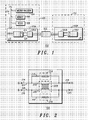
- FIG. 1 is a block diagram of an exemplary computing system
- FIG. 2 is a block diagram of an exemplary filter.
- a filter for an input/output port achieves improved electromagnetic filtering response by providing separate current paths for differential and single-ended signals.
- a common mode choke is provided as a filter for relatively high-frequency differential signals.
- one or more ferrites, inductors or other filter elements are provided in parallel to the choke to filter lower-frequency single-ended signals.
- an exemplary computing system 100 suitably includes a digital computer 102 that communicates with an external device 112 across communications medium 122.
- computer 102 is a personal computer and external device 112 is a peripheral device such as a digital camera, printer, scanner, input device, audio/visual device or the like.
- Computer 102 and external device 112 suitably exchange data via medium 122 using any protocol or convention, such as USB 1.1, USB 2.0, IEEE 1394, Ethernet, serial, parallel, or any other communications technique presently known or hereafter developed.
- any protocol or convention such as USB 1.1, USB 2.0, IEEE 1394, Ethernet, serial, parallel, or any other communications technique presently known or hereafter developed.
- various embodiments of communications medium 122 may encompass any type of cable, direct connection, wireless connection, cradle connection or the like.
- Computer 102 is any processing device such as a personal computer, workstation, personal digital assistant, wireless phone, portable computer, video game system or the like.
- Computer 102 includes appropriate data processing components for the particular implementation, including a microprocessor 104, digital memory 106, optional video card 108 and/or other components that communicate via a data bus 114 or other interconnect as appropriate.
- Computer 102 also includes an input/output (I/O) port 110A that provides an interface to communications medium 122 and to external device 112.
- Device 112 also includes an appropriate input/output port 110B to support communications over medium 122.
- Each I/O port 110A-B suitably includes a port controller 116 and a filter 120. As shown in Figure 1, elements 116A and 120A are associated with I/O port 110A, and elements 116B and 120B are associated with I/O port 110B. Although implementations of I/O ports 110A and 110B are described herein as being identical, the invention is not so limited. Indeed, in practice different devices 102/112 may include implementations of I/O ports 110 with widely varying components and architectures.
- Port controller 116 is any circuit or component capable of transmitting and receiving data via communications medium 122. Port controller 116 also communicates with processor 104 or any other components in computer 102 via bus 114. Accordingly, port controller 116 may be implemented with any processor, digital signal processor or controller capable of converting data from bus 114 into a format that can be transported by medium 122. Port controller 116 may be implemented as an application specific integrated circuit (ASIC), for example, that communicates with a transceiver (not shown) suited for the particular protocols transported on medium 122. In one embodiment, port controller 116 includes a USB controller available from, for example, Motorola Inc.
- ASIC application specific integrated circuit
- port controller 116 converts data between protocols used on bus 114 (e.g. the peripheral component interconnect (PCI) protocol) and those used on media 122.
- PCI peripheral component interconnect
- Many data protocols transmit data using "differential signals", which generally encode data based upon voltage differences between two transmitted electrical signals. Differential signals are generally less susceptible to noise than "single-ended signals” that encode data based upon voltage differences between a transmitted electrical signal and a reference voltage.
- port controller 116 typically supports two data signals "D+" and "D-" that are transmitted and received on two data lines 124 and 126, respectively, across medium 122.
- controller 116 suitably computes a voltage difference between signal "D+” received on signal line 124 and signal “D-” received on signal line 126.
- Many data protocols incorporate “combination signaling", which includes both single-ended and differential signals on signal lines 124 and 126.
- a controller 116 for a USB port 110 typically converts bus data to a differential signal represented by differences in voltages passed on signals D+ and D-.
- End of packet (EOP) indicators in the USB protocol are appropriately appended to the end of each data transmission as a single-ended signal provided on either or both of signal lines D+ and D-, and other single-ended signals may also be present.
- EOP End of packet
- Filter 120 is any circuit or device capable of reducing or removing noise, electromagnetic interference (EMI) or other unwanted components of signals transmitted or received by I/O port 110.
- Filter 120 is suitably designed to attenuate unwanted portions of signals D+ and D- while having only minimal effects upon the signals themselves.
- the transmitted signals may contain both differential and single-ended components, filter 120 suitably provides multiple current paths for the different types of signals, as described more fully below.
- each of the paths contains a filtering element appropriate for removing EMI and/or noise from either a high or low frequency signal corresponding to a differential or single-ended signal, respectively. Accordingly, relatively high-attenuation filters can be provided for the differential signals, resulting in improved EMI and/or noise filtering.
- an exemplary filter 120 suitably includes a differential mode signal path 202 and one or more single-ended signal paths 210, 212.
- Single-ended paths 210, 212 are shown wired in parallel with differential path 202 so that signals of varying frequencies and waveforms are appropriately filtered and processed.
- Each signal path 202, 210, 212 includes an appropriate filtering element 208, 204, 206 (respectively) such as an inductor, choke, ferrite or the like that is selected to remove EMI and/or noise from signals D+ and/or D- without degrading the quality of the signals themselves.
- differential mode current path 202 suitably includes a relatively broad-spectrum filtering element 208, whereas single-ended current paths 210, 212 contain filtering elements 204, 206 that are tuned to pass relatively low frequency signals. Accordingly, EMI and other noise from signal lines 124, 126 can be effectively reduced while both differential and single-ended signals are effectively passed through I/O port 110 ( Figure 1).
- FIG. 2 shows current paths 202, 210 and 212 as variously connecting input terminals 214 and 216, respectively, to output terminals 218 and 220, respectively.
- Terminal refers to any electrical node whatsoever, and may or may not include an interface for external connection or monitoring. Accordingly, while the discussion of input terminals 214, 216 and output terminals 218, 220 is presented herein for conceptualization and ease of explanation, each of these nodes are intended as logical concepts. In a practical embodiment, input terminals 214 and 216 may represent any point or node on signal lines 124 and 126 on the input side of filter 120, and output terminals 218 and 220 may represent any point or node on signal lines 124 and 126 on the output side of filter 120.
- terminals 214 and 216 may function as input terminals while data is being transmitted and as output terminals when data is being received.
- terminals 218 and 220 may function as both input and output terminals, depending on whether the particular I/O port 110 is transmitting or receiving data.
- Differential signal path 202 is any current path or set of paths that is capable of transmitting differential electrical signals.
- Differential signal path 202 is typically implemented using multiple signal paths (e.g. wires or other carriers) such that each component of the differential signal may be simultaneously passed to the receiver.
- signal paths e.g. wires or other carriers
- a differential "1" logic state is denoted by the D+ signal line voltage remaining at least 200 millivolts above the D- signal voltage.
- a differential "0" logic state is denoted by the D+ signal voltage remaining at least 200 millivolts below the D-signal voltage.
- Differential signals may be provided at a relatively high data rate, and may therefore require a relatively large amount of bandwidth.
- differential signal path 202 therefore includes a differential mode filter 208 that is capable of passing a relatively broad spectrum of differential signals such as a common mode choke.
- differential mode filter 208 is implemented with a model DLW31SN222SQ2 common mode choke available from the Murata Manufacturing Co. of Kyoto, Japan. While this particular choke is a relatively high attenuation component with impedance on the order of about 2.2 kOhms at 100MHz, other models of chokes or other filtering components having a wide range of specifications could be used to implement other embodiments of filtering element 208.
- Single-ended signal paths 210 and 212 are any current paths or sets of paths that are capable of transmitting single-ended electrical signals. Each single-ended signal path 210, 212 is typically implemented using a single carrier, since the transmitted signal is intended to be compared to a reference signal available at the receiver. As shown in Figure 2, single-ended paths 210 and 212 are configured in parallel connection to differential path 202 for each signal line 124 and 126, respectively. In alternate embodiments, only one single-ended signal line 124 or 126 may be required.
- an end-of-packet (EOP) condition may be represented with a single-ended zero (SE0) signal that is out-of-band and asynchronous to the in-band differential signaling discussed above.
- SE0 single-ended zero
- the bandwidth requirements of single-ended filtering elements 204, 206 are correspondingly lower than those for differential filtering element 208.
- filtering elements 204, 206 are implemented with ferrites or other filters commonly used with USB version 1.1 implementations, such as the model BLM15BD601 ferrite available from Murata Manufacturing Co. Of course other models of ferrites, inductors or other filters having a wide range of specifications could be used to implement other embodiments of filtering elements 204 and 206.
- filter 120 processes differential and single-ended signals received at input terminals 214 and 216 along separate paths to output terminals 218, 220.
- In-band differential signals are appropriately provided to a common-mode choke or other differential filter 208, which suitably reduces or removes EMI and/or noise produced by signal lines 124, 126 and/or other sources.
- Single-ended signals are simultaneously provided to one or more ferrites or other single-ended filters provided in parallel to the differential filter. Accordingly, both differential and single-ended signals are effectively passed through filter 120 without significant degradation or distortion.
- the terms "high-attenuation” and “broad spectrum” filter as used herein refer to filters with impedance in excess of about 150-200 ohms, and possibly as high as about 3 kOhms or even higher.
- Low attenuation filters, as described herein typically exhibit impedances of about 90 ohms as commonly used in many prior art implementations of USB version 2.0.
- broad spectrum filtering was not previously available for filtering combination signals because the high attenuation tended to distort the single-ended waveforms passing through the filter.
- the attenuation of the in-band path 202 can be greatly increased, thus resulting in greatly improved EMI and/or noise reduction in filter 120 and improved performance in I/O port 110.
Landscapes
- Filters And Equalizers (AREA)
- Networks Using Active Elements (AREA)
- Dc Digital Transmission (AREA)
Abstract
Description
Claims (10)
- An electromagnetic interference filter (120) for an input/output port transmitting both differential signals and single-ended signals between first and second input terminals and first and second output terminals, the filter characterized by:a differential mode filter (208) electrically coupled to the input terminals and to the output terminals, wherein the differential mode filter is operable to reduce electromagnetic interference while passing the differential signals; anda single-ended filter (204) electrically coupled to the input terminals and to the output terminals in parallel with the differential mode filter, wherein the single-ended filter is operable to reduce electromagnetic interference while passing single-ended signals.
- The filter of claim 1 wherein the single-ended filter characterized by a first signal path coupled to the first input terminal and to the first output terminal and a second signal path coupled to the second input terminal to the second output terminal.
- A circuit for filtering electromagnetic interference between first and second input terminals and first and second output terminals of an input/output port, the circuit characterized by:a high-frequency differential signal path electrically coupling the input terminals and the output terminals, the differential signal path comprising a broad spectrum filter;a first low-frequency signal path coupling the first input terminal to the first output terminal in parallel connection to the differential mode signal path and comprising a first filtering element; anda second low-frequency signal path coupling the second input terminal to the second output terminal in parallel connection to the differential mode signal path and comprising a second filtering element.
- A circuit for filtering electromagnetic interference between first and second input terminals and first and second output terminals of an input/output port, the circuit characterized by:a differential signal path electrically coupling the input terminals and the output terminals, the differential signal path comprising a high attenuation common-mode choke;a first single-ended signal path coupling the first input terminal to the first output terminal in parallel connection to the differential signal path and comprising a first ferrite; anda second single-ended signal path coupling the second input terminal to the second output terminal in parallel connection to the differential signal path and comprising a second ferrite.
- An input/output port having a first and a second input terminal and a first and a second output terminal, the input/output port characterized by:a differential signal path electrically coupling the input terminals and the output terminals, the high-frequency signal path comprising a common mode choke;a first single-ended signal path coupling the first input terminal to the first output terminal in parallel connection to the differential filter path and comprising a first filtering element; anda second single-ended signal path coupling the second input terminal to the second output terminal in parallel connection to the high frequency filter path and comprising a second filtering element.
- A computing system having a processor, a memory and an input/output port, wherein the input/output port characterized by:a first and a second input terminal;a first and a second output terminal;a differential signal path electrically coupling the input terminals and the output terminals, the high-frequency signal path comprising a common mode choke;a first single-ended signal path coupling the first input terminal to the first output terminal in parallel connection to the differential signal path and comprising a first filtering element; anda second single-ended signal path coupling the second input terminal to the second output terminal in parallel connection to the differential signal path and comprising a second filtering element.
- An electromagnetic interference filter for an input/output port transmitting both differential signals and single-ended signals between first and second input terminals and first and second output terminals, the filter characterized by:means for filtering the differential signal electrically coupled to the input terminals and to the output terminals and configured to reduce electromagnetic interference in the differential signals; andmeans for filtering the single-ended signals coupled in parallel with the means for filtering the differential signal, and being configured to reduce electromagnetic interference in the single-ended signals.
- A method of removing electromagnetic interference from an input signal comprising a differential portion and a single-ended portion, the method characterized by:receiving the input signal at a first and a second input terminals;providing the input signal to a differential signal filter to reduce electromagnetic interference from the differential portion; andproviding the input signal to a single-ended filter coupled in parallel with the differential filter to reduce electromagnetic interference in the single-ended portion of the input signal.
- The method of claim 8 wherein the differential filter is characterized by a common-mode choke.
- The method of claim 9 wherein the choke is a broad spectrum choke.
Applications Claiming Priority (2)
| Application Number | Priority Date | Filing Date | Title |
|---|---|---|---|
| US288795 | 2002-11-05 | ||
| US10/288,795 US6781481B2 (en) | 2002-11-05 | 2002-11-05 | Methods and apparatus for filtering electromagnetic interference from a signal in an input/output port |
Publications (2)
| Publication Number | Publication Date |
|---|---|
| EP1418651A2 true EP1418651A2 (en) | 2004-05-12 |
| EP1418651A3 EP1418651A3 (en) | 2006-08-02 |
Family
ID=32107629
Family Applications (1)
| Application Number | Title | Priority Date | Filing Date |
|---|---|---|---|
| EP03103979A Withdrawn EP1418651A3 (en) | 2002-11-05 | 2003-10-27 | Methods and apparatus for filtering electromagnetic interference from a signal in an input/output port |
Country Status (3)
| Country | Link |
|---|---|
| US (1) | US6781481B2 (en) |
| EP (1) | EP1418651A3 (en) |
| CA (1) | CA2447404A1 (en) |
Cited By (1)
| Publication number | Priority date | Publication date | Assignee | Title |
|---|---|---|---|---|
| CN104135148A (en) * | 2014-07-17 | 2014-11-05 | 青岛歌尔声学科技有限公司 | USB (Universal Serial Bus) interface circuit |
Families Citing this family (26)
| Publication number | Priority date | Publication date | Assignee | Title |
|---|---|---|---|---|
| US20080207197A1 (en) | 1997-07-30 | 2008-08-28 | Steven Tischer | Apparatus, method, and computer-readable medium for interfacing devices with communications networks |
| US7149514B1 (en) | 1997-07-30 | 2006-12-12 | Bellsouth Intellectual Property Corp. | Cellular docking station |
| US7194083B1 (en) | 2002-07-15 | 2007-03-20 | Bellsouth Intellectual Property Corporation | System and method for interfacing plain old telephone system (POTS) devices with cellular networks |
| US6411802B1 (en) | 1999-03-15 | 2002-06-25 | Bellsouth Intellectual Property Management Corporation | Wireless backup telephone device |
| US7120454B1 (en) | 2001-12-26 | 2006-10-10 | Bellsouth Intellectual Property Corp. | Auto sensing home base station for mobile telephone with remote answering capabilites |
| US8416804B2 (en) | 2002-07-15 | 2013-04-09 | At&T Intellectual Property I, L.P. | Apparatus and method for providing a user interface for facilitating communications between devices |
| US8543098B2 (en) | 2002-07-15 | 2013-09-24 | At&T Intellectual Property I, L.P. | Apparatus and method for securely providing communications between devices and networks |
| US8526466B2 (en) | 2002-07-15 | 2013-09-03 | At&T Intellectual Property I, L.P. | Apparatus and method for prioritizing communications between devices |
| US8275371B2 (en) | 2002-07-15 | 2012-09-25 | At&T Intellectual Property I, L.P. | Apparatus and method for providing communications and connection-oriented services to devices |
| US8000682B2 (en) | 2002-07-15 | 2011-08-16 | At&T Intellectual Property I, L.P. | Apparatus and method for restricting access to data |
| US7200424B2 (en) | 2002-07-15 | 2007-04-03 | Bellsouth Intelectual Property Corporation | Systems and methods for restricting the use and movement of telephony devices |
| US8554187B2 (en) | 2002-07-15 | 2013-10-08 | At&T Intellectual Property I, L.P. | Apparatus and method for routing communications between networks and devices |
| US7057475B2 (en) * | 2003-10-22 | 2006-06-06 | Adc Dsl Systems, Inc. | Ferrite choke |
| US8938021B1 (en) | 2004-05-06 | 2015-01-20 | Paul Shala Henry | Outbound interference reduction in a broadband powerline system |
| JP3962735B2 (en) * | 2004-09-07 | 2007-08-22 | Tdk株式会社 | Signal transmission circuit, electronic equipment, cable, and connector |
| US20060111886A1 (en) * | 2004-11-23 | 2006-05-25 | Mahesh Siddappa | Method and system for modeling of a differential bus device |
| US7336904B2 (en) * | 2004-11-29 | 2008-02-26 | Finisar Corporation | Electro-magnetic interference reduction filter for an optical transceiver |
| DE102006003379B4 (en) * | 2006-01-24 | 2011-02-24 | Infineon Technologies Ag | Electric filter |
| FI20060769A7 (en) * | 2006-08-28 | 2008-02-29 | Tellabs Oy | General purpose physical data transfer port |
| US8089266B2 (en) * | 2008-08-06 | 2012-01-03 | Robert Bosch Gmbh | Measuring induced currents on a CAN bus |
| TWI475395B (en) * | 2011-09-28 | 2015-03-01 | Htc Corp | Hand-held electrical apparatus and data transmission method thereof |
| TWI562718B (en) * | 2012-06-05 | 2016-12-11 | Ind Tech Res Inst | Emi shielding device and manufacturing method thereof |
| TWI540594B (en) * | 2013-09-10 | 2016-07-01 | 緯創資通股份有限公司 | Transmission line and filtering module thereof |
| US10374572B2 (en) * | 2016-10-14 | 2019-08-06 | John Gordon Ramsey | Radiofrequency filter with improved attenuation of common mode signals |
| US10170874B1 (en) * | 2017-09-14 | 2019-01-01 | Te Connectivity Corporation | Cable assembly having a substrate with multiple passive filtering devices between two sections of the cable assembly |
| US11476707B2 (en) | 2020-10-06 | 2022-10-18 | Apple Inc. | Wireless power system housing |
Family Cites Families (6)
| Publication number | Priority date | Publication date | Assignee | Title |
|---|---|---|---|---|
| US4801827A (en) * | 1987-11-02 | 1989-01-31 | Tektronix, Inc. | Adjustable delay element for digital systems |
| US5319343A (en) * | 1990-08-21 | 1994-06-07 | Powercube Corporation | Integrated magnetic inductor having series and common mode windings |
| US5243308A (en) * | 1992-04-03 | 1993-09-07 | Digital Equipment Corporation | Combined differential-mode and common-mode noise filter |
| US5313176A (en) * | 1992-10-30 | 1994-05-17 | Motorola Lighting, Inc. | Integrated common mode and differential mode inductor device |
| US5559396A (en) * | 1994-10-14 | 1996-09-24 | Philips Electronics North America Inc. | Ballast filtering scheme for reduced harmonic distortion |
| JPH11122909A (en) * | 1997-10-16 | 1999-04-30 | Fuji Electric Co Ltd | Noise filter for power converter |
-
2002
- 2002-11-05 US US10/288,795 patent/US6781481B2/en not_active Expired - Lifetime
-
2003
- 2003-10-27 EP EP03103979A patent/EP1418651A3/en not_active Withdrawn
- 2003-10-31 CA CA002447404A patent/CA2447404A1/en not_active Abandoned
Cited By (2)
| Publication number | Priority date | Publication date | Assignee | Title |
|---|---|---|---|---|
| CN104135148A (en) * | 2014-07-17 | 2014-11-05 | 青岛歌尔声学科技有限公司 | USB (Universal Serial Bus) interface circuit |
| CN104135148B (en) * | 2014-07-17 | 2018-01-12 | 青岛歌尔声学科技有限公司 | A kind of usb circuit |
Also Published As
| Publication number | Publication date |
|---|---|
| CA2447404A1 (en) | 2004-05-05 |
| US6781481B2 (en) | 2004-08-24 |
| EP1418651A3 (en) | 2006-08-02 |
| US20040085157A1 (en) | 2004-05-06 |
Similar Documents
| Publication | Publication Date | Title |
|---|---|---|
| US6781481B2 (en) | Methods and apparatus for filtering electromagnetic interference from a signal in an input/output port | |
| US5799040A (en) | Method for transmitting and/or receiving data at different data transfer rates especially in applications such as dual-rate ethernet local-area networks | |
| JP2002204272A (en) | Signal transmission device and signal transmission system | |
| US20110038286A1 (en) | Using frequency divisional multiplexing for a high speed serializer/deserializer with back channel communication | |
| DE112007001045B4 (en) | Method and system for reducing radiation emissions from a communication channel | |
| KR101696887B1 (en) | Usb connector for wireless communication device | |
| KR102802275B1 (en) | Termination for high frequency transmission lines | |
| CN101938316A (en) | Information detection device and method | |
| CN109039964B (en) | Circuit for correcting signal susceptible to baseline drift | |
| CN112019206A (en) | Digital isolator | |
| US8737521B2 (en) | Signal conversion during transmission of serial data streams | |
| JP4837715B2 (en) | Active connector | |
| EP2613487B1 (en) | Common-mode termination within communication systems | |
| KR100515316B1 (en) | Impedance matching apparatus and noise removing filter equipped with it | |
| CN212812003U (en) | Automobile audio transmission circuit | |
| JP2005523591A (en) | Apparatus and method for bias compensation in differential transmission line | |
| CN101799973A (en) | Signal transmission circuit and method | |
| CN117837090A (en) | EMI Cancellation for Wired Receivers with Safety Functions | |
| CN110730556B (en) | High-speed circuit and low-frequency reduction passive equalizer | |
| EP0958654B1 (en) | Passive analog filter for network interface | |
| US11728778B2 (en) | Differential signaling transmission systems | |
| CN217902443U (en) | Cross-network information transmission device based on image recognition | |
| JPWO2007080691A1 (en) | Data transmission system, receiver, and data transmission method using them | |
| CN118868983A (en) | Signal receiving device, signal processing method and electronic equipment | |
| US20040225807A1 (en) | Method and assembly having a matched filter connector |
Legal Events
| Date | Code | Title | Description |
|---|---|---|---|
| PUAI | Public reference made under article 153(3) epc to a published international application that has entered the european phase |
Free format text: ORIGINAL CODE: 0009012 |
|
| AK | Designated contracting states |
Kind code of ref document: A2 Designated state(s): AT BE BG CH CY CZ DE DK EE ES FI FR GB GR HU IE IT LI LU MC NL PT RO SE SI SK TR |
|
| AX | Request for extension of the european patent |
Extension state: AL LT LV MK |
|
| PUAL | Search report despatched |
Free format text: ORIGINAL CODE: 0009013 |
|
| AK | Designated contracting states |
Kind code of ref document: A3 Designated state(s): AT BE BG CH CY CZ DE DK EE ES FI FR GB GR HU IE IT LI LU MC NL PT RO SE SI SK TR |
|
| AX | Request for extension of the european patent |
Extension state: AL LT LV MK |
|
| 17P | Request for examination filed |
Effective date: 20060919 |
|
| 17Q | First examination report despatched |
Effective date: 20061201 |
|
| AKX | Designation fees paid |
Designated state(s): DE FR GB |
|
| 17Q | First examination report despatched |
Effective date: 20061201 |
|
| STAA | Information on the status of an ep patent application or granted ep patent |
Free format text: STATUS: THE APPLICATION IS DEEMED TO BE WITHDRAWN |
|
| 18D | Application deemed to be withdrawn |
Effective date: 20100504 |