EP1416691A1 - I/Q imbalance correction in a quadrature transceiver - Google Patents
I/Q imbalance correction in a quadrature transceiver Download PDFInfo
- Publication number
- EP1416691A1 EP1416691A1 EP02024392A EP02024392A EP1416691A1 EP 1416691 A1 EP1416691 A1 EP 1416691A1 EP 02024392 A EP02024392 A EP 02024392A EP 02024392 A EP02024392 A EP 02024392A EP 1416691 A1 EP1416691 A1 EP 1416691A1
- Authority
- EP
- European Patent Office
- Prior art keywords
- calibration coefficients
- phase
- carrier frequency
- quadrature
- larger
- Prior art date
- Legal status (The legal status is an assumption and is not a legal conclusion. Google has not performed a legal analysis and makes no representation as to the accuracy of the status listed.)
- Granted
Links
- 238000012937 correction Methods 0.000 title claims description 15
- 238000000034 method Methods 0.000 claims abstract description 30
- 238000012935 Averaging Methods 0.000 claims abstract description 4
- 238000012545 processing Methods 0.000 claims description 12
- 238000012360 testing method Methods 0.000 claims description 9
- 230000005540 biological transmission Effects 0.000 claims 1
- 238000006243 chemical reaction Methods 0.000 description 14
- 238000010586 diagram Methods 0.000 description 7
- 230000010354 integration Effects 0.000 description 6
- 230000001427 coherent effect Effects 0.000 description 5
- 230000006870 function Effects 0.000 description 5
- 238000004422 calculation algorithm Methods 0.000 description 4
- 230000000694 effects Effects 0.000 description 4
- 238000007476 Maximum Likelihood Methods 0.000 description 3
- 238000009825 accumulation Methods 0.000 description 3
- 230000003044 adaptive effect Effects 0.000 description 3
- 238000013459 approach Methods 0.000 description 3
- 238000004891 communication Methods 0.000 description 2
- 230000006735 deficit Effects 0.000 description 2
- 238000004088 simulation Methods 0.000 description 2
- 238000004364 calculation method Methods 0.000 description 1
- 230000001419 dependent effect Effects 0.000 description 1
- 238000009795 derivation Methods 0.000 description 1
- 230000007774 longterm Effects 0.000 description 1
- 238000012805 post-processing Methods 0.000 description 1
- 238000005070 sampling Methods 0.000 description 1
- 238000001228 spectrum Methods 0.000 description 1
- 230000009466 transformation Effects 0.000 description 1
Images


Classifications
-
- H—ELECTRICITY
- H04—ELECTRIC COMMUNICATION TECHNIQUE
- H04L—TRANSMISSION OF DIGITAL INFORMATION, e.g. TELEGRAPHIC COMMUNICATION
- H04L27/00—Modulated-carrier systems
- H04L27/0014—Carrier regulation
-
- H—ELECTRICITY
- H03—ELECTRONIC CIRCUITRY
- H03C—MODULATION
- H03C3/00—Angle modulation
- H03C3/38—Angle modulation by converting amplitude modulation to angle modulation
- H03C3/40—Angle modulation by converting amplitude modulation to angle modulation using two signal paths the outputs of which have a predetermined phase difference and at least one output being amplitude-modulated
-
- H—ELECTRICITY
- H03—ELECTRONIC CIRCUITRY
- H03D—DEMODULATION OR TRANSFERENCE OF MODULATION FROM ONE CARRIER TO ANOTHER
- H03D3/00—Demodulation of angle-, frequency- or phase- modulated oscillations
- H03D3/007—Demodulation of angle-, frequency- or phase- modulated oscillations by converting the oscillations into two quadrature related signals
- H03D3/009—Compensating quadrature phase or amplitude imbalances
-
- H—ELECTRICITY
- H04—ELECTRIC COMMUNICATION TECHNIQUE
- H04L—TRANSMISSION OF DIGITAL INFORMATION, e.g. TELEGRAPHIC COMMUNICATION
- H04L27/00—Modulated-carrier systems
- H04L27/0014—Carrier regulation
- H04L2027/0016—Stabilisation of local oscillators
-
- H—ELECTRICITY
- H04—ELECTRIC COMMUNICATION TECHNIQUE
- H04L—TRANSMISSION OF DIGITAL INFORMATION, e.g. TELEGRAPHIC COMMUNICATION
- H04L27/00—Modulated-carrier systems
- H04L27/0014—Carrier regulation
- H04L2027/0018—Arrangements at the transmitter end
-
- H—ELECTRICITY
- H04—ELECTRIC COMMUNICATION TECHNIQUE
- H04L—TRANSMISSION OF DIGITAL INFORMATION, e.g. TELEGRAPHIC COMMUNICATION
- H04L27/00—Modulated-carrier systems
- H04L27/0014—Carrier regulation
- H04L2027/0024—Carrier regulation at the receiver end
- H04L2027/0026—Correction of carrier offset
- H04L2027/003—Correction of carrier offset at baseband only
Definitions
- the underlying invention generally relates to the field of coherent modulator architectures for the processing of modulated RF signals of digital communication, systems, especially to a processing unit realizing an effective I/Q imbalance correction for high-level modulation schemes, e.g. 16-QAM or 64-QAM under the coexistence of a carrier frequency error.
- a processing unit realizing an effective I/Q imbalance correction for high-level modulation schemes, e.g. 16-QAM or 64-QAM under the coexistence of a carrier frequency error.
- Coherent modulators are applied in communication systems which are composed of both in-phase (I) and quadrature (Q) channels.
- I in-phase
- Q quadrature
- I/Q imbalance arises.
- high-level modulation schemes e.g. 16-QAM, 64-QAM or 256-QAM
- said I/Q imbalance introduces severe performance loss.
- an adequate calibration procedure conducting an I/Q imbalance correction has to be applied to adapt the gain of the I channel to that of the Q channel, and, simultaneously, to adjust the phase difference between the I channel and the Q channel to ⁇ /2.
- the first article provides the basic mathematical mode and a simple algorithm for DC offset cancellation and I/Q mismatch correction.
- the performance of this algorithm is confirmed by a simulation of the I/Q mismatch introduced by the gain and phase imbalance of quadrature mixers.
- the second article illustrates a complex Least Mean Square (LMS) algorithm and an adaptive noise canceller to separate the desired signal and the image noise introduced by the I/Q mismatch.
- LMS Least Mean Square
- the third article presents a Maximum-Likelihood (ML) solution for a gain imbalance estimation in a quadrature receiver, which can be used for array processing applications.
- formula derivations and simulations are provided to check the performance.
- all these papers only describe conventional I/Q impairment correction procedures without considering the coexistence of carrier frequency errors.
- the US-patent 5,705,949 is directed to a time-domain based calibration method for compensating the imbalance of the amplitude and phase between the I and the Q channel, in which correctable I/Q imbalance errors occurring in a complex receiver can be detected and digitally compensated without the use of special calibration signals.
- differential DC offset errors are compensated by averaging the incoming I and Q signals and subtracting expected values of differential DC offsets, e.g. computed from the long-term average of the I and Q signals, in order to create new I and Q signals.
- Differential gain imbalance errors are corrected by calculating a Root Mean Square (RMS) average of the new I and Q signals and using compensation coefficients which are determined from either the RMS average or by a Stochastic Gradient Algorithm.
- RMS Root Mean Square
- the European patent application EP 0 608 577 A1 pertains to a Gaussian Minimum Shift Keying (GMSK) modulator with an automatic calibration, wherein I and Q signals are generated in a baseband processing unit and sent to a phase modulator.
- GMSK Gaussian Minimum Shift Keying
- a time-domain based calibration method for compensating the imbalance of the amplitude and phase between the I and the Q channel is disclosed.
- the power of the transmitted signal can advantageously be used to detect DC offsets, quadrature errors and I/Q imbalances. All these sorts of errors are sequentially corrected by means of three separate control loops, and three separate control signals are generated. In this connection, the control loops share a common power detector, thus reducing the required chip area.
- the US patent 5,872,538 pertains to a frequency-domain based correction method for calibrating the imbalance of the amplitude and phase between the I and the Q signal obtained by the I/Q demodulator of a quadrature receiver, which is directly performed by exploiting the symmetry properties of the Discrete Fourier Transform (DFT) of a real signal, taking the in-phase component as the real part and the quadrature component as the imaginary part.
- DFT Discrete Fourier Transform
- the European patent application EP 0 984 288 A1 refers to a wideband I/Q splitting apparatus to be used in a spectrum analyzer and an appropriate time-domain based calibration method, which is used for calibrating the group difference between the I and the Q channel.
- the proposed approach according to the underlying invention is dedicated to a novel calibration procedure for an I/Q modulator, which supports a compensation of amplitude offsets and phase imbalances and furthermore considers the coexistence of a carrier frequency error in order to obtain a set of accurate and reliable calibration coefficients.
- a specially designed processing unit is integrated within the I/Q modulator.
- the invention can advantageously be applied when high-level modulation schemes, e.g. 16-QAM or 64-QAM, are used.
- the transmitter output for Q channel after band-pass filter is given by
- the output signal of the I channel of the RX part yields and the output signal of the Q channel of the RX part yields
- ⁇ c is the phase of the carrier relative to the test waveform in the receiver (RX) part
- f co denotes the cut-off frequency of the low-pass filters 112a+b applied to the I/Q demodulator 101' (101") depicted in Figs. 1 and 3, respectively.
- FIG. 2 A block diagram of a circuitry applied to the I/Q modulator, which illustrates said online I/Q imbalance compensation procedure, is shown in Fig. 2.
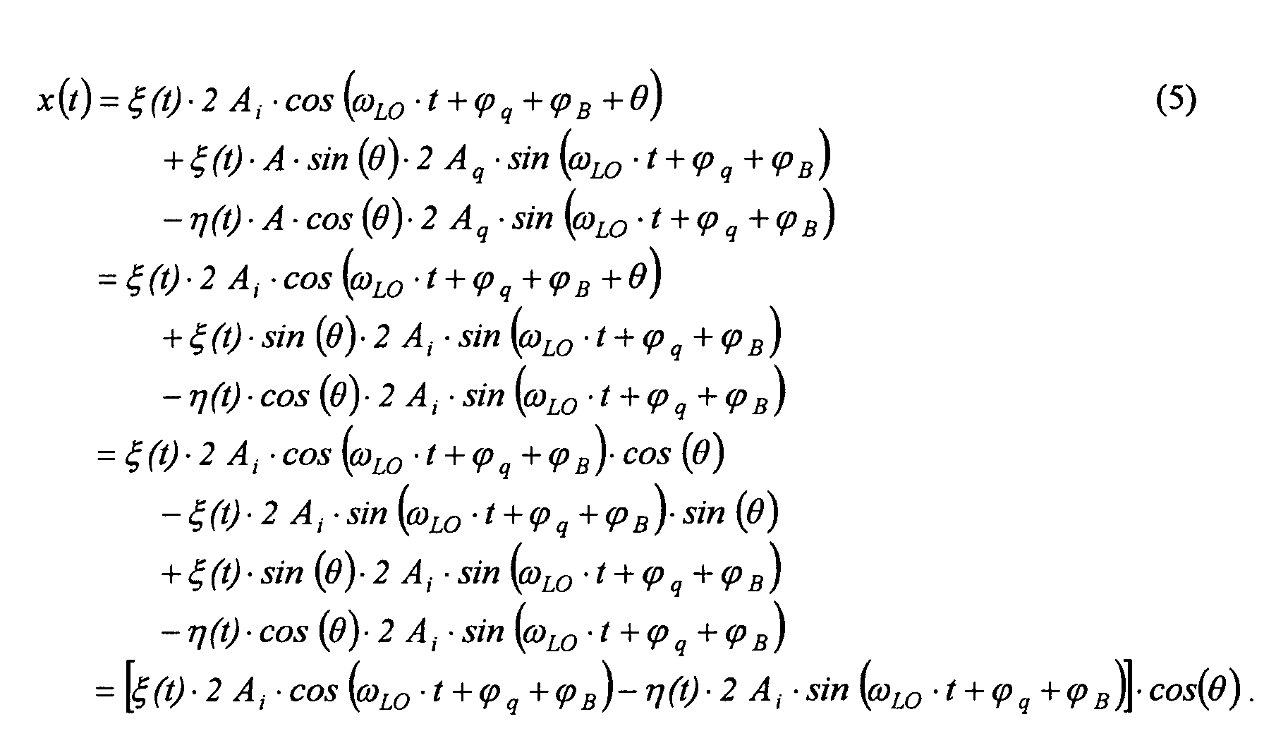
- the practical RF signal to be transmitted is given by the following equation, wherein ⁇ ( t ) and ⁇ (t) are the practical I and Q channel input signals instead of the previously applied test waveforms i(t) and q(t) introduced in Fig. 1:
- M is limited to integer values smaller than the upper threshold value M max calculated by equation (6) due to the existence of the carrier frequency error ⁇ f RF .
- this dilemma can be solved by applying a so-called non-coherent accumulation of the calculated calibration coefficients based on equation (6) and a small number of samples.
- the detailed information is summarized as follows:
- noise reduction can be achieved by using a large number of M ⁇ K samples, and the effect of carrier frequency error ⁇ f RF can be reduced by using a small number of M samples.
- reliable calibration coefficients can be obtained by considering the coexistence of noise and carrier frequency error.
- a novel calibration structure according to one embodiment of the underlying invention as depicted in Fig. 3 is proposed, wherein a simple frequency error estimation block 306 is included.
- Conventional adaptive frequency error correction includes two parts: an acquisition module which limits the frequency error to a predefined range and a more complex tracking module which further reduces the frequency error in order to satisfy the system requirement.
- a simple frequency acquisition module is recommended to use, that provides only a rough estimation of the carrier frequency error ⁇ f RF .
- it fulfills the following two functions:
- the calibration function explained above is modified by replacing the circular frequency ⁇ LO generated by a local oscillator by the term ⁇ LO + ⁇ ⁇ and LO , wherein ⁇ and LO denotes an estimated frequency offset value.
- This frequency offset ⁇ and LO is stored in a memory when the circuit is turned off and used as the initial value of the frequency offset value when the circuit is turned on.
- the value of M can gradually be increased from the beginning of the calibration iteration (step #1), and the number of iterations ( K ) can be reduced.
- the following carrier update functions are applied: 2 cos ( ⁇ LO ⁇ t + ⁇ C ) is replaced by 2 cos [( ⁇ LO + ⁇ ⁇ LO ) ⁇ t + ⁇ C ] -2 sin ( ⁇ LO ⁇ t + ⁇ C ) is replaced by - 2 sin [ ( ⁇ LO + ⁇ ⁇ LO ) ⁇ t + ⁇ C ] for ⁇ ⁇ LO ⁇ ⁇ ⁇ LO , min, wherein ⁇ and LO, min denotes a predefined threshold value in order to avoid the fluctuation of the frequency adjustment caused by background noise, etc.
- the same idea can be used for the I/Q demodulator instead of the I/Q modulator to conduct an I/Q imbalance correction for high-level modulation schemes, e.g. 16-QAM or 64-QAM, under the coexistence of a carrier frequency error.
- Depicted Features and their Associated Reference Signs No. Technical Features and System Components 100 block diagram showing a practical I/Q modulator 100' applied to a quadrature transmitter and an ideal I/Q demodulator 101' applied to a quadrature receiver according to the underlying invention 100' I/Q modulator of a first mobile transceiver according to a first embodiment of the underlying invention depicted in Fig.
Landscapes
- Engineering & Computer Science (AREA)
- Computer Networks & Wireless Communication (AREA)
- Signal Processing (AREA)
- Power Engineering (AREA)
- Digital Transmission Methods That Use Modulated Carrier Waves (AREA)
Abstract
Description
- Fig. 1
- presents a block diagram showing a practical I/Q modulator applied to a quadrature transmitter and an ideal I/Q demodulator applied to a quadrature receiver according to the underlying invention,
- Fig. 2
- depicts a block diagram of an analog circuitry applied to the I/Q modulator of a quadrature transmitter executing an online I/Q imbalance compensation procedure according to one embodiment of the underlying invention, and
- Fig. 3
- presents a block diagram showing an I/Q modulator applied to a quadrature transmitter and an I/Q demodulator applied to a quadrature receiver, which illustrates a calibration procedure executing an I/Q imbalance compensation considering the existence of a carrier frequency error according to the underlying invention.


- Ai
- denotes the amplitude of a signal generated by a local oscillator (LO) for the I channel,
- Aq
- denotes the amplitude of a signal generated by a local oscillator (LO) for the Q channel,
- ϕi and ϕq
- are used to model the phase discrepancies between the I and the Q channel,
- ωLO
- denotes a circular frequency generated by a local oscillator (LO), and
- ϕB
- is the phase of the carrier relative to the test waveform in the transmitter (TX) part.







- A
- denotes the amplitude imbalance ratio between the I and the Q signal and
-
- is the phase discrepancy between the I and the Q signal.

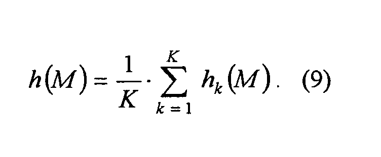
- Steps #1:
- For k = 1 to K: Using the [(k-1)·M]-th to the (k·M-1)-th sample from a set of M · K samples to calculate the calibration coefficients hk (M).
- Step #2:
- Calculate the calibration coefficient as the arithmetic mean of said
calibration coefficients hk (M) according to the following formula:
| Depicted Features and their Associated Reference Signs | |
| No. | Technical Features and System Components |
| 100 | block diagram showing a practical I/Q modulator 100' applied to a quadrature transmitter and an ideal I/Q demodulator 101' applied to a quadrature receiver according to the underlying invention |
| 100' | I/Q modulator of a first mobile transceiver according to a first embodiment of the underlying invention depicted in Fig. 1, realized as a quadrature transmitter |
| 100" | I/Q modulator of a first mobile transceiver according to a second embodiment of the underlying invention depicted in Fig. 3, realized as a quadrature transmitter |
| 101' | I/Q demodulator of a second mobile transceiver according to a first embodiment of the underlying invention depicted in Fig. 1, realized as a quadrature receiver |
| 101" | I/Q demodulator of a second mobile transceiver according to a second embodiment of the underlying invention depicted in Fig. 3, realized as a quadrature receiver |
| 102a | summation element in the I chain of the I/Q modulator 100', which is used for modeling the DC offset of the I signal |
| 102b | summation element in the Q chain of the I/Q modulator 100', which is used for modeling the DC offset of the Q signal |
| 104a | up-conversion mixer in the I chain of the I/Q modulator 100'/100", which realizes a direct up-conversion of the I signal from the baseband to the passband by multiplying said I signal with a CW signal originating from a local oscillator (LO) |
| 104b | up-conversion mixer in the Q chain of the I/Q modulator 100'/100", which realizes a direct up-conversion of the Q signal from the baseband to the passband by multiplying said Q signal with a CW signal originating from a local oscillator (LO) |
| 106a | band-pass filter (BPF) in the I chain of the I/Q modulator 100'/100" |
| 106b | band-pass filter (BPF) in the Q chain of the I/Q modulator 100'/100" |
| 108 | summation element at the output port of the I/Q modulator 100'/100" |
| 110a | down-conversion mixer in the I chain of the I/Q demodulator 101'/101", which realizes a direct down-conversion of the received RF signal from the passband to the baseband by multiplying said RF signal with a CW signal originating from a local oscillator (LO) |
| 110b | down-conversion mixer in the Q chain of the I/Q demodulator 101'/101", which realizes a direct down-conversion of the received RF signal from the passband to the baseband by multiplying said RF signal with a CW signal originating from a local oscillator (LO) |
| 112a | low-pass filter (LPF) in the I chain of the I/Q demodulator 101'/101" |
| 112b | low-pass filter (LPF) in the Q chain of the I/Q demodulator 101'/101" |
| 200 | block diagram of an analog circuitry applied to the I/Q modulator 100'/100" of a quadrature transmitter executing an online I/Q imbalance, compensation procedure according to one embodiment of the underlying invention |
| 202a | first multiplier of the analog circuitry 200 |
| 202b | second multiplier of the analog circuitry 200 |
| 204 | first summation element of the analog circuitry 200 |
| 206a | up-conversion mixer in the I chain of the analog circuitry 200, which realizes a direct up-conversion of the I signal from the baseband to the passband by multiplying said I signal with a CW signal originating from a local oscillator (LO) |
| 206b | up-conversion mixer in the Q chain of the analog circuitry 200, which realizes a direct up-conversion of the Q signal from the baseband to the passband by multiplying said Q signal with a CW signal originating from a local oscillator (LO) |
| 208 | second summation element of the analog circuitry 200 |
| 300 | block diagram showing an I/Q modulator 100'/100" applied to a quadrature transmitter and an I/Q demodulator 101'/101" applied to a quadrature receiver, which illustrates a calibration procedure executing an I/Q imbalance compensation considering the existence of a carrier frequency error according to the underlying invention |
| 302 | calibration unit for iteratively calculating calibration coefficients hk (M) needed for conducting an I/Q imbalance correction and DC offset cancellation procedure according to one embodiment of the underlying invention, based on M samples per integration period T |
| 304 | unit for a non-coherent accumulation of the iteratively calculated calibration coefficients hk (M) |
| 306 | unit for an estimation of the carrier frequency error Δf RF |
| 308 | unit for the calculation of the maximum number of samples (Mmax) per integration period T according to equation (15) |
| 310a | unit providing the carrier update function 2 cos [(ωLO +Δω and LO · t + ϕC ] fed to the down- |
| 310b | unit providing the carrier update function - 2 sin [(ωLO +Δω andLO · t + ϕC ] fed to the down- |
Claims (9)
- An I/Q calibration method for reducing the influences of a carrier frequency error (Δf RF), wherein the amplitude and phase of in-phase (I) and quadrature (Q) signals are corrected by using calibration coefficients (h(M)) in order to reduce I/Q imbalances, the method comprising the following steps in order to calculate the calibration coefficients (h(M)):wherein the averaged calibration coefficients (h(M)) are used to correct the in-phase (I) and quadrature (Q) signals.a) using a number of M samples in order to calculate initial calibration coefficients (hk(M)), M being an integer value larger than 1, andb) calculating averaged calibration coefficients (h(M)) by averaging a plurality of said initial calibration coefficients (hk(M)) obtained by repeating step a) for a limited number of K repetitions, K being an integer value larger than 1,
- A method according to claim 1,
wherein the signals cos (ω0 · t) and sin (ω0 · t) are used as test waveforms for the in-phase (I) signal and the quadrature (Q) signal in a mobile transmitter and/or mobile receiver of a wireless transmission system, respectively, and the number of M samples is observed and evaluated within a predefined time period given by the size T of a time window,
characterized in that
the window size T is an integer multiple of the fundamental time period T0 = 2π / ω 0 of the test waveforms cos (ω0 · t) and sin (ω0 · t), which is larger than 1, wherein ω0 denotes the circular frequency of said test waveforms. - A method according to anyone of the preceding claims,
characterized in that
the value of M is set based on a carrier frequency estimation, the value of M being set the larger the smaller the estimated carrier frequency error (Δf RF )· - A method according to claim 3,
characterized in that
the number of repetitions (K) is set the larger the smaller the value of the number of signal samples (M). - An I/Q modulator,
comprising a processing unit (302) for correcting the amplitude and phase of the in-phasewherein the processing unit (302) is designed to calculate the averaged calibration coefficients (h(M)) to correct the in-phase (I) and quadrature (Q) signals.(I) and quadrature (Q) signals by calculating calibration coefficients (h (M)) in order to reduce I/Q imbalances,
the processing unit (302) being designed to carry out the following steps in order to calculate the calibration coefficients (h (M)):a) using a number of M signal samples in order to calculate initial calibration coefficients (hk (M)), M being an integer value larger than 1, andb) calculating averaged calibration coefficients (h (M)) by averaging a plurality of said initial calibration coefficients (hk (M)) obtained by repeating step a) for a limited number of K repetitions, K being an integer value larger than 1, - An I/Q modulator according to claim 5,
characterized by
a carrier frequency estimation unit (306), wherein the processing unit (302) is designed to set the value of M based on an output signal of the carrier frequency estimation unit (306), the value of M being set the larger the smaller the estimated carrier frequency error (Δf RF). - An I/Q modulator according to anyone of the claims 5 or 6,
characterized in that
the processing unit (302) is designed to set the number of repetitions (K) the larger the smaller the value of the number of signal samples (M). - A method for operating an I/Q modulator (100', 100") according to anyone of the claims 5 to 7,
characterized in that
the current carrier frequency estimation valueis stored in a non-volatile memory when the circuit (200) executing said I/Q calibration method is switched off and reused in a subsequent switching on of said circuit (200) in order to increase the number of samples (M) from the beginning of a method according to anyone of the claims 1 to 4.
- An I/Q demodulator according to anyone of the claims 1 to 8
being specially adapted to conduct an I/Q imbalance correction under the coexistence of a carrier frequency error (ΔfRF).
Priority Applications (2)
| Application Number | Priority Date | Filing Date | Title |
|---|---|---|---|
| EP20020024392 EP1416691B1 (en) | 2002-11-04 | 2002-11-04 | I/Q imbalance correction in a quadrature transceiver |
| DE2002609983 DE60209983T2 (en) | 2002-11-04 | 2002-11-04 | Correction of I / Q inequalities in a quadrature transceiver |
Applications Claiming Priority (1)
| Application Number | Priority Date | Filing Date | Title |
|---|---|---|---|
| EP20020024392 EP1416691B1 (en) | 2002-11-04 | 2002-11-04 | I/Q imbalance correction in a quadrature transceiver |
Publications (2)
| Publication Number | Publication Date |
|---|---|
| EP1416691A1 true EP1416691A1 (en) | 2004-05-06 |
| EP1416691B1 EP1416691B1 (en) | 2006-03-22 |
Family
ID=32087995
Family Applications (1)
| Application Number | Title | Priority Date | Filing Date |
|---|---|---|---|
| EP20020024392 Expired - Lifetime EP1416691B1 (en) | 2002-11-04 | 2002-11-04 | I/Q imbalance correction in a quadrature transceiver |
Country Status (2)
| Country | Link |
|---|---|
| EP (1) | EP1416691B1 (en) |
| DE (1) | DE60209983T2 (en) |
Cited By (14)
| Publication number | Priority date | Publication date | Assignee | Title |
|---|---|---|---|---|
| EP1643635A2 (en) | 2004-09-17 | 2006-04-05 | Motorola, Inc. | Demodulator for use in wireless communications and receiver, method and terminal using it |
| WO2010014989A2 (en) | 2008-08-01 | 2010-02-04 | Qualcomm Incorporated | Upconverter and downconverter with switched transconductance and lo masking |
| US7822399B2 (en) | 2007-05-11 | 2010-10-26 | Telefonaktiebolaget Lm Ericsson (Publ) | Image compensation for wireless receiver |
| US7894555B2 (en) | 2007-08-02 | 2011-02-22 | Telefonaktiebolaget Lm Ericsson (Publ) | IQ imbalance image suppression |
| US7986930B2 (en) | 2007-08-02 | 2011-07-26 | Telefonaktiebolaget Lm Ericsson (Publ) | IQ imbalance image suppression in presence of unknown phase shift |
| EP2223485B1 (en) * | 2007-12-18 | 2013-06-12 | Qualcomm Incorporated | I-q mismatch calibration and method |
| US8712357B2 (en) | 2008-11-13 | 2014-04-29 | Qualcomm Incorporated | LO generation with deskewed input oscillator signal |
| US8717077B2 (en) | 2008-11-25 | 2014-05-06 | Qualcomm Incorporated | Duty cycle adjustment for a local oscillator signal |
| US8791740B2 (en) | 2009-07-16 | 2014-07-29 | Qualcomm Incorporated | Systems and methods for reducing average current consumption in a local oscillator path |
| US8847638B2 (en) | 2009-07-02 | 2014-09-30 | Qualcomm Incorporated | High speed divide-by-two circuit |
| US8854098B2 (en) | 2011-01-21 | 2014-10-07 | Qualcomm Incorporated | System for I-Q phase mismatch detection and correction |
| US8970272B2 (en) | 2008-05-15 | 2015-03-03 | Qualcomm Incorporated | High-speed low-power latches |
| US9154077B2 (en) | 2012-04-12 | 2015-10-06 | Qualcomm Incorporated | Compact high frequency divider |
| CN111490959A (en) * | 2020-04-03 | 2020-08-04 | 北京力通通信有限公司 | IQ imbalance correction method, device and circuit for broadband multi-channel radio frequency transceiver |
Citations (1)
| Publication number | Priority date | Publication date | Assignee | Title |
|---|---|---|---|---|
| US5705949A (en) * | 1996-09-13 | 1998-01-06 | U.S. Robotics Access Corp. | Compensation method for I/Q channel imbalance errors |
-
2002
- 2002-11-04 EP EP20020024392 patent/EP1416691B1/en not_active Expired - Lifetime
- 2002-11-04 DE DE2002609983 patent/DE60209983T2/en not_active Expired - Fee Related
Patent Citations (1)
| Publication number | Priority date | Publication date | Assignee | Title |
|---|---|---|---|---|
| US5705949A (en) * | 1996-09-13 | 1998-01-06 | U.S. Robotics Access Corp. | Compensation method for I/Q channel imbalance errors |
Non-Patent Citations (1)
| Title |
|---|
| PIERRE J W ET AL: "CONSIDERATIONS IN THE AUTOCALIBRATION OF QUADRATURE RECEIVERS", PROCEEDINGS OF THE INTERNATIONAL CONFERENCE ON ACOUSTICS, SPEECH, AND SIGNAL PROCESSING (ICASSP). DETROIT, MAY 9 - 12, 1995. STATISTICAL SIGNAL AND ARRAY PROCESSING, NEW YORK, IEEE, US, vol. 3 CONF. 20, 9 May 1995 (1995-05-09), pages 1900 - 1903, XP000533080, ISBN: 0-7803-2432-3 * |
Cited By (18)
| Publication number | Priority date | Publication date | Assignee | Title |
|---|---|---|---|---|
| EP1643635A3 (en) * | 2004-09-17 | 2007-10-24 | Motorola, Inc. | Demodulator for use in wireless communications and receiver, method and terminal using it |
| GB2419483B (en) * | 2004-09-17 | 2008-12-24 | Motorola Inc | Demodulator for use in wireless communucations and receiver, method and terminal using it |
| EP1643635A2 (en) | 2004-09-17 | 2006-04-05 | Motorola, Inc. | Demodulator for use in wireless communications and receiver, method and terminal using it |
| US7822399B2 (en) | 2007-05-11 | 2010-10-26 | Telefonaktiebolaget Lm Ericsson (Publ) | Image compensation for wireless receiver |
| US7986930B2 (en) | 2007-08-02 | 2011-07-26 | Telefonaktiebolaget Lm Ericsson (Publ) | IQ imbalance image suppression in presence of unknown phase shift |
| US7894555B2 (en) | 2007-08-02 | 2011-02-22 | Telefonaktiebolaget Lm Ericsson (Publ) | IQ imbalance image suppression |
| US8615205B2 (en) | 2007-12-18 | 2013-12-24 | Qualcomm Incorporated | I-Q mismatch calibration and method |
| EP2223485B1 (en) * | 2007-12-18 | 2013-06-12 | Qualcomm Incorporated | I-q mismatch calibration and method |
| US8970272B2 (en) | 2008-05-15 | 2015-03-03 | Qualcomm Incorporated | High-speed low-power latches |
| WO2010014989A2 (en) | 2008-08-01 | 2010-02-04 | Qualcomm Incorporated | Upconverter and downconverter with switched transconductance and lo masking |
| US8712357B2 (en) | 2008-11-13 | 2014-04-29 | Qualcomm Incorporated | LO generation with deskewed input oscillator signal |
| US8717077B2 (en) | 2008-11-25 | 2014-05-06 | Qualcomm Incorporated | Duty cycle adjustment for a local oscillator signal |
| US8718574B2 (en) | 2008-11-25 | 2014-05-06 | Qualcomm Incorporated | Duty cycle adjustment for a local oscillator signal |
| US8847638B2 (en) | 2009-07-02 | 2014-09-30 | Qualcomm Incorporated | High speed divide-by-two circuit |
| US8791740B2 (en) | 2009-07-16 | 2014-07-29 | Qualcomm Incorporated | Systems and methods for reducing average current consumption in a local oscillator path |
| US8854098B2 (en) | 2011-01-21 | 2014-10-07 | Qualcomm Incorporated | System for I-Q phase mismatch detection and correction |
| US9154077B2 (en) | 2012-04-12 | 2015-10-06 | Qualcomm Incorporated | Compact high frequency divider |
| CN111490959A (en) * | 2020-04-03 | 2020-08-04 | 北京力通通信有限公司 | IQ imbalance correction method, device and circuit for broadband multi-channel radio frequency transceiver |
Also Published As
| Publication number | Publication date |
|---|---|
| DE60209983D1 (en) | 2006-05-11 |
| DE60209983T2 (en) | 2006-12-21 |
| EP1416691B1 (en) | 2006-03-22 |
Similar Documents
| Publication | Publication Date | Title |
|---|---|---|
| US8526518B2 (en) | Imbalance compensation for direct conversion communication systems | |
| US6934341B2 (en) | Method and apparatus for plurality signal generation | |
| EP1505723B1 (en) | Hybrid distortion compensation method and hybrid distortion compensation apparatus | |
| US6940916B1 (en) | Wideband analog quadrature modulator/demodulator with pre-compensation/post-compensation correction | |
| US7532873B2 (en) | DC offset cancellation in a zero IF receiver | |
| EP1214795B1 (en) | Apparatus for interference compensation of a direct conversion transceiver and method | |
| EP1416691B1 (en) | I/Q imbalance correction in a quadrature transceiver | |
| US8923461B2 (en) | Method and faculty to measure and compensate DCO frequency distortions using a DPLL | |
| US7174146B2 (en) | Method and apparatus for I/Q mismatch calibration in a receiver | |
| US8867596B2 (en) | Methods and apparatuses of calibrating I/Q mismatch in communication circuit | |
| US20060062324A1 (en) | Distortion compensation quadrature modulator and radio transmitter | |
| EP2181533B1 (en) | IQ imbalance image suppression in presence of unknown phase shift | |
| EP1502402A1 (en) | Magnitude and phase imbalance calibration and compensation in quadrature receivers | |
| US20100232490A1 (en) | Method and apparatus for compensating a modulation imbalance effect in a communication device | |
| US10819540B2 (en) | Radio frequency impairments compensator for broadband quadrature-conversion architectures | |
| EP0937339B1 (en) | Calibration of n-port receiver | |
| EP3174225A1 (en) | Apparatus and methods for phase synchronization of local oscillators in a transceiver | |
| US7310388B2 (en) | Direct conversion receiver and receiving method | |
| EP2261686B1 (en) | Method and apparatus for measuring signal phase shifts | |
| EP2547059B1 (en) | Transmitter including calibration of an in-phase/Quadrature (I/Q) modulator and associated methods | |
| KR100489409B1 (en) | Method for improving a performance of transmitter and receiver in wireless communication systems | |
| US20040049717A1 (en) | Frequency error detector and combiner in receiving end of mobile communication system | |
| Rykaczewski et al. | Blind I/Q imbalance compensation in multipath environments | |
| US20040208264A1 (en) | System and method of low power demodulation of continuous phase modulated waveforms | |
| US20040032919A1 (en) | Enhanced DC offset mitigation |
Legal Events
| Date | Code | Title | Description |
|---|---|---|---|
| PUAI | Public reference made under article 153(3) epc to a published international application that has entered the european phase |
Free format text: ORIGINAL CODE: 0009012 |
|
| AK | Designated contracting states |
Kind code of ref document: A1 Designated state(s): AT BE BG CH CY CZ DE DK EE ES FI FR GB GR IE IT LI LU MC NL PT SE SK TR |
|
| AX | Request for extension of the european patent |
Extension state: AL LT LV MK RO SI |
|
| 17P | Request for examination filed |
Effective date: 20041006 |
|
| AKX | Designation fees paid |
Designated state(s): DE FR GB |
|
| 17Q | First examination report despatched |
Effective date: 20050111 |
|
| GRAP | Despatch of communication of intention to grant a patent |
Free format text: ORIGINAL CODE: EPIDOSNIGR1 |
|
| RAP1 | Party data changed (applicant data changed or rights of an application transferred) |
Owner name: SONY DEUTSCHLAND GMBH |
|
| RAP1 | Party data changed (applicant data changed or rights of an application transferred) |
Owner name: SONY DEUTSCHLAND GMBH |
|
| GRAS | Grant fee paid |
Free format text: ORIGINAL CODE: EPIDOSNIGR3 |
|
| RAP1 | Party data changed (applicant data changed or rights of an application transferred) |
Owner name: SONY DEUTSCHLAND GMBH |
|
| GRAA | (expected) grant |
Free format text: ORIGINAL CODE: 0009210 |
|
| AK | Designated contracting states |
Kind code of ref document: B1 Designated state(s): DE FR GB |
|
| REG | Reference to a national code |
Ref country code: GB Ref legal event code: FG4D |
|
| REF | Corresponds to: |
Ref document number: 60209983 Country of ref document: DE Date of ref document: 20060511 Kind code of ref document: P |
|
| ET | Fr: translation filed | ||
| PLBE | No opposition filed within time limit |
Free format text: ORIGINAL CODE: 0009261 |
|
| STAA | Information on the status of an ep patent application or granted ep patent |
Free format text: STATUS: NO OPPOSITION FILED WITHIN TIME LIMIT |
|
| 26N | No opposition filed |
Effective date: 20061227 |
|
| PGFP | Annual fee paid to national office [announced via postgrant information from national office to epo] |
Ref country code: DE Payment date: 20081103 Year of fee payment: 7 |
|
| PGFP | Annual fee paid to national office [announced via postgrant information from national office to epo] |
Ref country code: FR Payment date: 20081112 Year of fee payment: 7 |
|
| PGFP | Annual fee paid to national office [announced via postgrant information from national office to epo] |
Ref country code: GB Payment date: 20081029 Year of fee payment: 7 |
|
| GBPC | Gb: european patent ceased through non-payment of renewal fee |
Effective date: 20091104 |
|
| REG | Reference to a national code |
Ref country code: FR Ref legal event code: ST Effective date: 20100730 |
|
| PG25 | Lapsed in a contracting state [announced via postgrant information from national office to epo] |
Ref country code: FR Free format text: LAPSE BECAUSE OF NON-PAYMENT OF DUE FEES Effective date: 20091130 |
|
| PG25 | Lapsed in a contracting state [announced via postgrant information from national office to epo] |
Ref country code: DE Free format text: LAPSE BECAUSE OF NON-PAYMENT OF DUE FEES Effective date: 20100601 |
|
| PG25 | Lapsed in a contracting state [announced via postgrant information from national office to epo] |
Ref country code: GB Free format text: LAPSE BECAUSE OF NON-PAYMENT OF DUE FEES Effective date: 20091104 |