EP1416658A1 - Power efficient symbol processing - Google Patents
Power efficient symbol processing Download PDFInfo
- Publication number
- EP1416658A1 EP1416658A1 EP20020257509 EP02257509A EP1416658A1 EP 1416658 A1 EP1416658 A1 EP 1416658A1 EP 20020257509 EP20020257509 EP 20020257509 EP 02257509 A EP02257509 A EP 02257509A EP 1416658 A1 EP1416658 A1 EP 1416658A1
- Authority
- EP
- European Patent Office
- Prior art keywords
- processing system
- symbol rate
- rate processing
- data
- blocks
- Prior art date
- Legal status (The legal status is an assumption and is not a legal conclusion. Google has not performed a legal analysis and makes no representation as to the accuracy of the status listed.)
- Withdrawn
Links
- 238000012545 processing Methods 0.000 title claims abstract description 17
- 238000001228 spectrum Methods 0.000 claims abstract description 13
- 238000013459 approach Methods 0.000 claims abstract description 12
- 238000012937 correction Methods 0.000 claims abstract description 10
- 238000004891 communication Methods 0.000 claims abstract description 9
- 239000000945 filler Substances 0.000 claims description 2
- 230000001276 controlling effect Effects 0.000 description 4
- 230000006870 function Effects 0.000 description 4
- 230000011218 segmentation Effects 0.000 description 4
- 238000013501 data transformation Methods 0.000 description 3
- 230000005540 biological transmission Effects 0.000 description 2
- 238000001514 detection method Methods 0.000 description 2
- 238000005516 engineering process Methods 0.000 description 2
- 238000013507 mapping Methods 0.000 description 2
- 230000000052 comparative effect Effects 0.000 description 1
- 238000013506 data mapping Methods 0.000 description 1
- 238000003780 insertion Methods 0.000 description 1
- 230000037431 insertion Effects 0.000 description 1
- 238000012544 monitoring process Methods 0.000 description 1
- 230000002093 peripheral effect Effects 0.000 description 1
- 230000001105 regulatory effect Effects 0.000 description 1
Images


Classifications
-
- H—ELECTRICITY
- H04—ELECTRIC COMMUNICATION TECHNIQUE
- H04L—TRANSMISSION OF DIGITAL INFORMATION, e.g. TELEGRAPHIC COMMUNICATION
- H04L1/00—Arrangements for detecting or preventing errors in the information received
- H04L1/004—Arrangements for detecting or preventing errors in the information received by using forward error control
- H04L1/0056—Systems characterized by the type of code used
- H04L1/0067—Rate matching
- H04L1/0068—Rate matching by puncturing
-
- H—ELECTRICITY
- H04—ELECTRIC COMMUNICATION TECHNIQUE
- H04L—TRANSMISSION OF DIGITAL INFORMATION, e.g. TELEGRAPHIC COMMUNICATION
- H04L1/00—Arrangements for detecting or preventing errors in the information received
- H04L1/004—Arrangements for detecting or preventing errors in the information received by using forward error control
- H04L1/0041—Arrangements at the transmitter end
-
- H—ELECTRICITY
- H04—ELECTRIC COMMUNICATION TECHNIQUE
- H04L—TRANSMISSION OF DIGITAL INFORMATION, e.g. TELEGRAPHIC COMMUNICATION
- H04L1/00—Arrangements for detecting or preventing errors in the information received
- H04L1/004—Arrangements for detecting or preventing errors in the information received by using forward error control
- H04L1/0045—Arrangements at the receiver end
-
- H—ELECTRICITY
- H04—ELECTRIC COMMUNICATION TECHNIQUE
- H04L—TRANSMISSION OF DIGITAL INFORMATION, e.g. TELEGRAPHIC COMMUNICATION
- H04L1/00—Arrangements for detecting or preventing errors in the information received
- H04L1/004—Arrangements for detecting or preventing errors in the information received by using forward error control
- H04L1/0056—Systems characterized by the type of code used
- H04L1/0071—Use of interleaving
Definitions
- the present invention is related to a receiver for IMT-2000 spread-spectrum signals, more particularly to the implementation of the 3G UMTS outer modem functionality.
- Channel coding is the combination of error detection, error correction, rate matching, interleaving and transport channel mapping onto physical channels.
- Most implementations of the outer modem are mainly software procedures controlling hardware accelerators (hardware blocks with one specific task, e.g. Viterbi or turbo codecs). This means the software handles the data, i.e. the software swaps the data between different hardware accelerators. This is called a DSP centric approach. Disadvantages of this approach are:
- the present invention aims to provide a novel implementation of an outer modem for a spread spectrum transceiver.
- the present invention concerns a symbol rate processing system for high-speed spread spectrum communications arranged for operation at a specific data rate, comprising programmable hardware blocks running at specific clock frequencies, characterised in that said system comprises programmable registers and comprises means for interleaving, means for error correction and means for rate matching, wherein said clock frequencies are significantly less than the frequencies needed in a DSP-centric approach.
- the clock frequencies for the means for interleaving, error correction and rate matching are less than 50 times the data rate, preferably less than 40 times the data rate. Lower clock frequencies can also be used.
- the hardware implemented symbol rate processing system according to the present invention will be able to run at clock frequencies that are less than half of the clock frequency needed for the same functionality with a DSP centric approach.
- the means for error correction can comprise one or more elements of the group consisting of a convolutional encoder, a viterbi decoder, a turbo encoder and a turbo decoder.
- the programmable registers are controlled by a microprocessor subsystem.
- Said microprocessor subsystem preferably comprises one or more parameters selected from the group consisting of code block length, code rate for error codecs, number of code blocks to be processed, number of fillers to be inserted, numbers of bits to be punctured or repeated, number of iterations in turbo decoding, length of CRC, polynomials for codecs and separate enables/resets for blocks.
- the spread-spectrum communications are preferably selected from the group consisting of IMT-2000, 3GPP, 3GPP2, W-CDMA, UMTS/FDD, UMTS/TDD, 1xEV-DO, 1xEV-DV, CDMA2000, IS95, IS95A, IS95B, UWB, TD-SCDMA, LAS-CDMA, IEEE802.11, IEEE802.11A, IEEE802.11B or IEEE802.16 communications.
- an integrated circuit comprising the symbol rate processing system according to the present invention is disclosed.
- a further embodiment is a transceiver for high-speed spread spectrum communications comprising the symbol rate processing system according to the present invention.
- Fig. 1 represents a functional schematic view of an outer modem as used for spread spectrum transceivers.
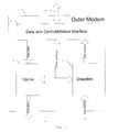
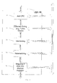
- Fig. 2, 3 and 4 respectively show the data and control & Status interface, the downlink block and the uplink block for the outer modem according to the invention.
- the maximum data rate refers to the maximum data speed of the user or application data stream that is delivered to the L1-2-3 protocol system of the air interface to consider.
- the "user” here is e.g. an application program that runs in layers above L3. This data rate will then e.g. still include all the overhead of e.g. an Internet Protocol connection. Also note that for WCDMA, data rate is not the chipping rate. Examples of data rates are 384 kbit/s for UMTS/FDD (mobile applications) and 2 Mbit/s for UMTS/TDD (Office applications)
- a transceiver for spread-spectrum comprises a RF part responsible for the transmission and reception of all spread-spectrum signals.
- the so-called inner modem On reception of such signals, the so-called inner modem is responsible for acquisition and demodulation of the raw data.
- the inner modem When transmitting, the inner modem is used for modulating the data into a spread-spectrum signal. In real-life implementations, this means that an inner modem needs to cope with large data streams being received and sent by the transceiver.
- the signal that has been demodulated by the inner modem is not yet usable for the end user.
- the outer modem as can be seen in figure 1, comprises an uplink block 3 for preparing the data for transmission, a downlink block 5 which prepares received data for the end user, and a Data and Control & Status Interface 7 which allows control from a general purpose processor or DSP for both the downlink and uplink blocks and the data feed to and from the end user.
- the Data and Control & Status interface 7 is depicted in figure 2. It comprises buffer RAM memory 11 for both uplink and downlink, both data streams being regulated by a RAM arbiter 13. Both data streams are interfaced to a controlling unit by a physical bus interface (15).
- the Data and Control & Status interface 7 also allows control from a general-purpose processor or DSP for the interrupt handling and registers of the outer modem via the register set & interrupt handler (17).
- Downlink (5) and uplink (3) blocks are each other's opposites: while uplink block 3 (see fig. 3) comprises Data mapping 31, Ratematching 32, Interleaving 33, Channel coding 34 and CRC 35 blocks, all controlled through the Data and Control & Status interface 7, the downlink block 5 comprises blocks that do the opposite: Data unmapping 21, Unratematching 22, Deinterleaving 23, Channel decoding 24 and CRC check (25) blocks, again all controlled through the Data and Control & Status interface 7.
- Downlink and uplink are not necessarily symmetrical, for e.g. UMTS a non-symmetrical architecture can be used.
- the outer modem according to an embodiment of the present invention contains:
- control blocks are controlled by the following control blocks:
- Base band functionality comprises the inner and outer modem.
- DSP Digital Signal Processor
- peripherals and buses for accessing said DSP
- hardware accelerators such as viterbi, turbo, rake and modulator.
- DSP 1 and 2 are clocked at 200 MHz and produce 400 MIPS. Power consumption is respectively 0.72 and 0.25 mW/MIPS.
Landscapes
- Engineering & Computer Science (AREA)
- Computer Networks & Wireless Communication (AREA)
- Signal Processing (AREA)
- Mobile Radio Communication Systems (AREA)
- Error Detection And Correction (AREA)
Abstract
The present invention is related to a symbol
rate processing system for high-speed spread spectrum
communications arranged for operation at a specific data
rate, comprising programmable hardware blocks running at
specific clock frequencies, characterised in that said
system comprises programmable registers comprising means
for interleaving, means for error correction and means for
rate matching, wherein said clock frequencies are
significantly less than the frequencies needed in a DSP-centric
approach.
Description
- The present invention is related to a receiver for IMT-2000 spread-spectrum signals, more particularly to the implementation of the 3G UMTS outer modem functionality.
- In IMT-2000 receiver/transceiver technology, one can distinguish a so-called inner modem, and an outer modem. The basic function of the outer modem is channel coding. Channel coding is the combination of error detection, error correction, rate matching, interleaving and transport channel mapping onto physical channels.
- Most implementations of the outer modem are mainly software procedures controlling hardware accelerators (hardware blocks with one specific task, e.g. Viterbi or turbo codecs). This means the software handles the data, i.e. the software swaps the data between different hardware accelerators. This is called a DSP centric approach. Disadvantages of this approach are:
- There is a higher load on the processor because the processor can only execute general-purpose instructions and because of the data swapping. The consequence of a higher load is higher power consumption, which is undesirable in any mobile implementation.
- It is not efficient to implement some algorithms in software. An example of such an algorithm is interleaving.
- The present invention aims to provide a novel implementation of an outer modem for a spread spectrum transceiver.
- The present invention concerns a symbol rate processing system for high-speed spread spectrum communications arranged for operation at a specific data rate, comprising programmable hardware blocks running at specific clock frequencies, characterised in that said system comprises programmable registers and comprises means for interleaving, means for error correction and means for rate matching, wherein said clock frequencies are significantly less than the frequencies needed in a DSP-centric approach. Preferably, in the symbol rate processing system of the invention, the clock frequencies for the means for interleaving, error correction and rate matching are less than 50 times the data rate, preferably less than 40 times the data rate. Lower clock frequencies can also be used. In general, the hardware implemented symbol rate processing system according to the present invention will be able to run at clock frequencies that are less than half of the clock frequency needed for the same functionality with a DSP centric approach.
- In the symbol rate processing system according to the present invention, the means for error correction can comprise one or more elements of the group consisting of a convolutional encoder, a viterbi decoder, a turbo encoder and a turbo decoder.
- Preferably, the programmable registers are controlled by a microprocessor subsystem. Said microprocessor subsystem preferably comprises one or more parameters selected from the group consisting of code block length, code rate for error codecs, number of code blocks to be processed, number of fillers to be inserted, numbers of bits to be punctured or repeated, number of iterations in turbo decoding, length of CRC, polynomials for codecs and separate enables/resets for blocks.
- In the symbol rate processing system of the present invention, the spread-spectrum communications are preferably selected from the group consisting of IMT-2000, 3GPP, 3GPP2, W-CDMA, UMTS/FDD, UMTS/TDD, 1xEV-DO, 1xEV-DV, CDMA2000, IS95, IS95A, IS95B, UWB, TD-SCDMA, LAS-CDMA, IEEE802.11, IEEE802.11A, IEEE802.11B or IEEE802.16 communications.
- In a specific embodiment of the present invention, an integrated circuit comprising the symbol rate processing system according to the present invention is disclosed.
- A further embodiment is a transceiver for high-speed spread spectrum communications comprising the symbol rate processing system according to the present invention.
- Fig. 1 represents a functional schematic view of an outer modem as used for spread spectrum transceivers.
- Fig. 2, 3 and 4 respectively show the data and control & Status interface, the downlink block and the uplink block for the outer modem according to the invention.
- In the present invention, a hardware approach is proposed as the solution for the outer modem implementation. Some of the advantages are:
- High flexibility where needed: part of the outer modem can be configured by software.
- Low power consumption: dedicated hardware can run at a lower clock speed than a processor doing the same job in the same amount of time. This means the dedicated hardware uses less power than a DSP centric solution to execute the same functions.
- The maximum data rate refers to the maximum data speed of the user or application data stream that is delivered to the L1-2-3 protocol system of the air interface to consider. The "user" here is e.g. an application program that runs in layers above L3. This data rate will then e.g. still include all the overhead of e.g. an Internet Protocol connection. Also note that for WCDMA, data rate is not the chipping rate. Examples of data rates are 384 kbit/s for UMTS/FDD (mobile applications) and 2 Mbit/s for UMTS/TDD (Office applications)
- In general, a transceiver for spread-spectrum comprises a RF part responsible for the transmission and reception of all spread-spectrum signals. On reception of such signals, the so-called inner modem is responsible for acquisition and demodulation of the raw data. When transmitting, the inner modem is used for modulating the data into a spread-spectrum signal. In real-life implementations, this means that an inner modem needs to cope with large data streams being received and sent by the transceiver.
- The signal that has been demodulated by the inner modem is not yet usable for the end user. The
outer modem 1, as can be seen in figure 1, comprises anuplink block 3 for preparing the data for transmission, adownlink block 5 which prepares received data for the end user, and a Data and Control &Status Interface 7 which allows control from a general purpose processor or DSP for both the downlink and uplink blocks and the data feed to and from the end user. - The Data and Control &
Status interface 7 is depicted in figure 2. It comprisesbuffer RAM memory 11 for both uplink and downlink, both data streams being regulated by aRAM arbiter 13. Both data streams are interfaced to a controlling unit by a physical bus interface (15). The Data and Control &Status interface 7 also allows control from a general-purpose processor or DSP for the interrupt handling and registers of the outer modem via the register set & interrupt handler (17). - Downlink (5) and uplink (3) blocks are each other's opposites: while uplink block 3 (see fig. 3) comprises
Data mapping 31,Ratematching 32, Interleaving 33,Channel coding 34 andCRC 35 blocks, all controlled through the Data and Control &Status interface 7, thedownlink block 5 comprises blocks that do the opposite:Data unmapping 21, Unratematching 22, Deinterleaving 23,Channel decoding 24 and CRC check (25) blocks, again all controlled through the Data and Control &Status interface 7. Downlink and uplink are not necessarily symmetrical, for e.g. UMTS a non-symmetrical architecture can be used. - An implementation of an outer modem according to the present invention is given as an example:
The outer modem according to an embodiment of the present invention contains: - RAM in order to buffer data;
- software to configure, control and monitor the outer modem;
- A register set with configuration parameters and status bits. The configuration is written from software, the status bits can be read by software for controlling or monitoring the outer modem;
- Hardware blocks performing data transformations on the data stream. These blocks are in the data path, this means that data is passed between these blocks only;
- Hardware blocks controlling the blocks mentioned
above, no data is passing through these blocks.
These control blocks are configured by software via the register set. - Interfacing with L1 software, L2/L3 software. To interface with the software a set of registers is provided, as well as a mechanism for interrupt generation, and
- Interfacing with the inner modem.
- A general-purpose DSP/processor to execute the software.
- The following functions are provided in dedicated hardware blocks doing data transformations:
- CRC (error detection)
- Block segmentation
- Convolutional encoding, convolutional decoding (e.g. Viterbi decoding), (error correction)
- Turbo encoding/ decoding (error correction)
- Radio frame equalisation
- Rate matching
- Interleavers
- Transport channel multiplexing and physical channel segmentation
- Physical channel mapping.
- The above data transformation blocks are controlled by the following control blocks:
- L1, L2/L3 interface PVCI handler. This block controls the PVCI interface, register set and interrupt handling.
- The Transport Channel Controller controls the block segmentation, CRC, convolutional and turbo encoding/decoding.
- The Radio Frame Controller controls rate matching, interleavers, transport channel multiplexing and physical channel segmentation.
- Physical Channel Handling Controller (insertion of TFCI, Pilot bits and interfacing the inner modem).
- A power consumption estimate was made for the base band functionality of three model systems. Base band functionality comprises the inner and outer modem.
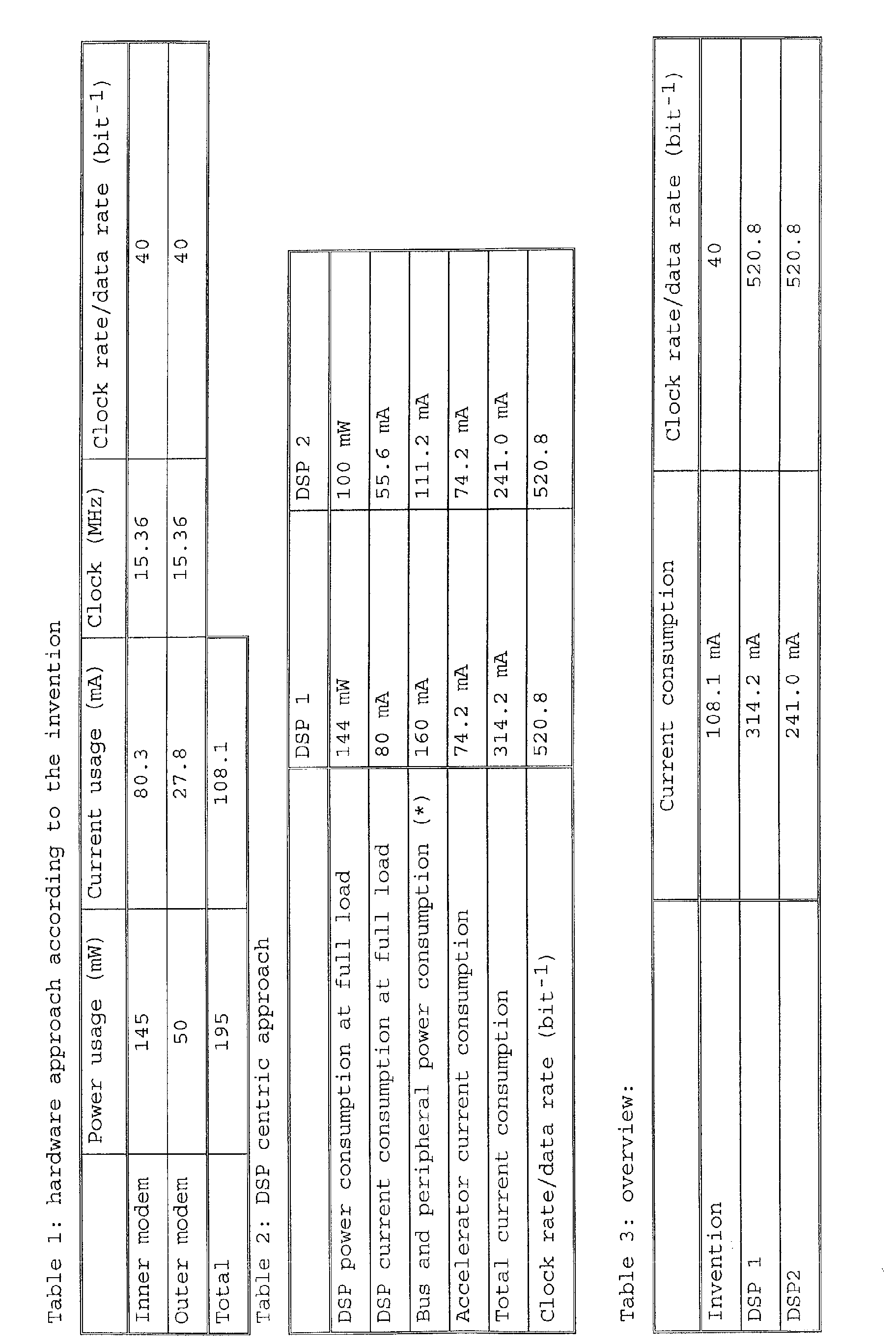
- For the hardware approach according to the present invention, 1,8V core voltage and 0,18µ CMOS technology is used for a 384 kbit/s data rate. Table 1 shows the power consumption of the different elements. Two DSP centric approaches are estimated, the details thereof are represented in table 2. The DSP centric approach requires a Digital Signal Processor (DSP), peripherals and buses for accessing said DSP, off-chip memory accesses, and hardware accelerators such as viterbi, turbo, rake and modulator.
DSP 1 and 2 are clocked at 200 MHz and produce 400 MIPS. Power consumption is respectively 0.72 and 0.25 mW/MIPS. - The results are summarised in table 3. It is clear that a DSP approach uses more current to perform the same function for the same data rate. This is mainly due to the fact that a higher clock frequency is needed for a DSP centric approach.
- Other data rates can of course be treated by the hardware symbol processor of the present invention. E.g., for a data rate of 2Mbit/s, a hardware clock frequency of about 60MHz has to be envisaged.
Claims (8)
- A symbol rate processing system for high-speed spread spectrum communications arranged for operation at a specific data rate, comprising programmable hardware blocks running at specific clock frequencies, characterised in that said system comprises programmable registers and comprises means for interleaving, means for error correction and means for rate matching, wherein said clock frequencies are significantly less than the frequencies needed in a DSP-centric approach.
- The symbol rate processing system as in claim 1, wherein the clock frequencies for the means for interleaving, error correction and rate matching are less than 50 times the data rate.
- The symbol rate processing system as in claim 1 or 2, wherein the means for error correction comprises one or more elements of the group consisting of a convolutional encoder, a Viterbi decoder, a turbo encoder and a turbo decoder.
- The symbol rate processing system as in any of the claim 1 to 3, wherein the programmable registers are controlled by a microprocessor subsystem.
- The symbol rate processing system as in claim 4, wherein the microprocessor subsystem comprises one or more parameters selected from the group consisting of code block length, code rate for error codecs, number of code blocks to be processed, number of fillers to be inserted, numbers of bits to be punctured or repeated, number of iterations in turbo decoding, length of CRC, polynomials for codecs and separate enables/resets for blocks.
- The symbol rate processing system as in any of the claims 1 to 5, wherein the spread-spectrum communications are selected from the group consisting of IMT-2000, 3GPP, 3GPP2, W-CDMA, UMTS/FDD, UMTS/TDD, 1xEV-DO, 1xEV-DV, CDMA2000, IS95, IS95A, IS95B, UWB, TD-SCDMA, LAS-CDMA, IEEE802.11, IEEE802.11A, IEEE802.11B or IEEE802.16 communications.
- An integrated circuit comprising the symbol rate processing system as in any of the claims 1 to 6.
- A transceiver for high-speed spread spectrum communications comprising the symbol rate processing system as in any of the claims 1 to 6.
Priority Applications (2)
| Application Number | Priority Date | Filing Date | Title |
|---|---|---|---|
| EP20020257509 EP1416658A1 (en) | 2002-10-30 | 2002-10-30 | Power efficient symbol processing |
| US10/695,688 US20040103358A1 (en) | 2002-10-30 | 2003-10-29 | Power efficient symbol processing |
Applications Claiming Priority (1)
| Application Number | Priority Date | Filing Date | Title |
|---|---|---|---|
| EP20020257509 EP1416658A1 (en) | 2002-10-30 | 2002-10-30 | Power efficient symbol processing |
Publications (1)
| Publication Number | Publication Date |
|---|---|
| EP1416658A1 true EP1416658A1 (en) | 2004-05-06 |
Family
ID=32088056
Family Applications (1)
| Application Number | Title | Priority Date | Filing Date |
|---|---|---|---|
| EP20020257509 Withdrawn EP1416658A1 (en) | 2002-10-30 | 2002-10-30 | Power efficient symbol processing |
Country Status (2)
| Country | Link |
|---|---|
| US (1) | US20040103358A1 (en) |
| EP (1) | EP1416658A1 (en) |
Cited By (3)
| Publication number | Priority date | Publication date | Assignee | Title |
|---|---|---|---|---|
| CN1320838C (en) * | 2004-07-19 | 2007-06-06 | 北京信威通信技术股份有限公司 | On-line monitoring syste mand method for radio receiving transmitting apparatus in SCDMA system |
| CN1320837C (en) * | 2004-07-19 | 2007-06-06 | 北京信威通信技术股份有限公司 | Real-time automatic calibrating method and system for radio base station array channel in SCDMA system |
| WO2008008512A3 (en) * | 2006-07-14 | 2008-04-10 | Interdigital Tech Corp | Symbol rate hardware accelerator |
Citations (2)
| Publication number | Priority date | Publication date | Assignee | Title |
|---|---|---|---|---|
| US20010004761A1 (en) * | 1997-05-30 | 2001-06-21 | Ephraim Zehavi | Method and apparatus for providing error protection for over the air file transfer |
| WO2001093431A2 (en) * | 2000-06-02 | 2001-12-06 | Qualcomm Inc | Method and apparatus for puncturing code symbols in a communications system |
Family Cites Families (1)
| Publication number | Priority date | Publication date | Assignee | Title |
|---|---|---|---|---|
| US7230978B2 (en) * | 2000-12-29 | 2007-06-12 | Infineon Technologies Ag | Channel CODEC processor configurable for multiple wireless communications standards |
-
2002
- 2002-10-30 EP EP20020257509 patent/EP1416658A1/en not_active Withdrawn
-
2003
- 2003-10-29 US US10/695,688 patent/US20040103358A1/en not_active Abandoned
Patent Citations (2)
| Publication number | Priority date | Publication date | Assignee | Title |
|---|---|---|---|---|
| US20010004761A1 (en) * | 1997-05-30 | 2001-06-21 | Ephraim Zehavi | Method and apparatus for providing error protection for over the air file transfer |
| WO2001093431A2 (en) * | 2000-06-02 | 2001-12-06 | Qualcomm Inc | Method and apparatus for puncturing code symbols in a communications system |
Non-Patent Citations (1)
| Title |
|---|
| KATSUHIKO UEDA ET AL: "A 16-BIT DIGITAL SIGNAL PROCESSOR WITH SPECIALLY ARRANGED MULTIPLY-ACCUMULATOR FOR LOW POWER CONSUMPTION", IEICE TRANSACTIONS ON ELECTRONICS, INSTITUTE OF ELECTRONICS INFORMATION AND COMM. ENG. TOKYO, JP, vol. E78-C, no. 12, 1 December 1995 (1995-12-01), pages 1709 - 1716, XP000555577, ISSN: 0916-8524 * |
Cited By (4)
| Publication number | Priority date | Publication date | Assignee | Title |
|---|---|---|---|---|
| CN1320838C (en) * | 2004-07-19 | 2007-06-06 | 北京信威通信技术股份有限公司 | On-line monitoring syste mand method for radio receiving transmitting apparatus in SCDMA system |
| CN1320837C (en) * | 2004-07-19 | 2007-06-06 | 北京信威通信技术股份有限公司 | Real-time automatic calibrating method and system for radio base station array channel in SCDMA system |
| WO2008008512A3 (en) * | 2006-07-14 | 2008-04-10 | Interdigital Tech Corp | Symbol rate hardware accelerator |
| US8015471B2 (en) | 2006-07-14 | 2011-09-06 | Interdigital Technology Corporation | Symbol rate hardware accelerator |
Also Published As
| Publication number | Publication date |
|---|---|
| US20040103358A1 (en) | 2004-05-27 |
Similar Documents
| Publication | Publication Date | Title |
|---|---|---|
| CN1647429B (en) | Wireless user equipment configured in TDD and FDD, base station and method | |
| WO2009052494A2 (en) | Wireless transmit/receive unit | |
| TW200539592A (en) | Method and apparatus for providing fast detection of a high speed shared control channel | |
| EP1410513A1 (en) | Channel codec processor configurable for multiple wireless communications standards | |
| JP2008507941A (en) | HSDPA coprocessor that upgrades the capabilities of existing modem hosts | |
| JP2010016861A (en) | Memory architecture for map decoder | |
| EP1657845A2 (en) | Dynamic retransmission mode selector | |
| US20040103358A1 (en) | Power efficient symbol processing | |
| CN101981852A (en) | Efficient parallel sub-packet decoding using multiple decoders, controller and task instructions | |
| CN101517911A (en) | Re-quantization in a downlink receiver bit rate processor | |
| US8042028B2 (en) | HS-PDSCH decoder and mobile radio-signal communication device including the same | |
| GB2408900A (en) | Receiver capable of rate de-matching data block-by-block | |
| JP2010004416A (en) | Mobile radio apparatus | |
| US20050243951A1 (en) | Iterative turbo decision feedback receiver | |
| CN110445516B (en) | Forward error correction code processing method and device | |
| CN205566651U (en) | Encrypt digital baseband control circuit based on gauss frequency shift keying wireless transceiver | |
| EP3761540A1 (en) | Mitigating viterbi decoder processing latency in wireless systems | |
| HK1074296A (en) | Software parameterizable control blocks for use in physical layer processing | |
| EP1751901B1 (en) | Transport channel decoding management in a umts mobile receiver | |
| Hocevar et al. | Programmable DSPs for 3G Base Station Modems | |
| Nikolic-Popovic | Application of Texas Instruments’ TMS320C6400 in 3G wireless infrastructure transceivers |
Legal Events
| Date | Code | Title | Description |
|---|---|---|---|
| PUAI | Public reference made under article 153(3) epc to a published international application that has entered the european phase |
Free format text: ORIGINAL CODE: 0009012 |
|
| AK | Designated contracting states |
Kind code of ref document: A1 Designated state(s): AT BE BG CH CY CZ DE DK EE ES FI FR GB GR IE IT LI LU MC NL PT SE SK TR |
|
| AX | Request for extension of the european patent |
Extension state: AL LT LV MK RO SI |
|
| 17P | Request for examination filed |
Effective date: 20041108 |
|
| AKX | Designation fees paid |
Designated state(s): DE GB |
|
| 17Q | First examination report despatched |
Effective date: 20050304 |
|
| STAA | Information on the status of an ep patent application or granted ep patent |
Free format text: STATUS: THE APPLICATION IS DEEMED TO BE WITHDRAWN |
|
| 18D | Application deemed to be withdrawn |
Effective date: 20060804 |