EP1416487A2 - Optical disk apparatus and phase adjustment method - Google Patents
Optical disk apparatus and phase adjustment method Download PDFInfo
- Publication number
- EP1416487A2 EP1416487A2 EP03254643A EP03254643A EP1416487A2 EP 1416487 A2 EP1416487 A2 EP 1416487A2 EP 03254643 A EP03254643 A EP 03254643A EP 03254643 A EP03254643 A EP 03254643A EP 1416487 A2 EP1416487 A2 EP 1416487A2
- Authority
- EP
- European Patent Office
- Prior art keywords
- signal
- recording
- delay
- binary
- clock signal
- Prior art date
- Legal status (The legal status is an assumption and is not a legal conclusion. Google has not performed a legal analysis and makes no representation as to the accuracy of the status listed.)
- Granted
Links
Images





Classifications
-
- G—PHYSICS
- G11—INFORMATION STORAGE
- G11B—INFORMATION STORAGE BASED ON RELATIVE MOVEMENT BETWEEN RECORD CARRIER AND TRANSDUCER
- G11B7/00—Recording or reproducing by optical means, e.g. recording using a thermal beam of optical radiation by modifying optical properties or the physical structure, reproducing using an optical beam at lower power by sensing optical properties; Record carriers therefor
- G11B7/004—Recording, reproducing or erasing methods; Read, write or erase circuits therefor
- G11B7/0045—Recording
-
- G—PHYSICS
- G11—INFORMATION STORAGE
- G11B—INFORMATION STORAGE BASED ON RELATIVE MOVEMENT BETWEEN RECORD CARRIER AND TRANSDUCER
- G11B20/00—Signal processing not specific to the method of recording or reproducing; Circuits therefor
- G11B20/10—Digital recording or reproducing
- G11B20/10009—Improvement or modification of read or write signals
- G11B20/10222—Improvement or modification of read or write signals clock-related aspects, e.g. phase or frequency adjustment or bit synchronisation
-
- G—PHYSICS
- G11—INFORMATION STORAGE
- G11B—INFORMATION STORAGE BASED ON RELATIVE MOVEMENT BETWEEN RECORD CARRIER AND TRANSDUCER
- G11B20/00—Signal processing not specific to the method of recording or reproducing; Circuits therefor
- G11B20/10—Digital recording or reproducing
- G11B20/10009—Improvement or modification of read or write signals
-
- G—PHYSICS
- G11—INFORMATION STORAGE
- G11B—INFORMATION STORAGE BASED ON RELATIVE MOVEMENT BETWEEN RECORD CARRIER AND TRANSDUCER
- G11B20/00—Signal processing not specific to the method of recording or reproducing; Circuits therefor
- G11B20/10—Digital recording or reproducing
- G11B20/10009—Improvement or modification of read or write signals
- G11B20/10305—Improvement or modification of read or write signals signal quality assessment
- G11B20/10398—Improvement or modification of read or write signals signal quality assessment jitter, timing deviations or phase and frequency errors
- G11B20/10425—Improvement or modification of read or write signals signal quality assessment jitter, timing deviations or phase and frequency errors by counting out-of-lock events of a PLL
-
- G—PHYSICS
- G11—INFORMATION STORAGE
- G11B—INFORMATION STORAGE BASED ON RELATIVE MOVEMENT BETWEEN RECORD CARRIER AND TRANSDUCER
- G11B2220/00—Record carriers by type
- G11B2220/20—Disc-shaped record carriers
-
- G—PHYSICS
- G11—INFORMATION STORAGE
- G11B—INFORMATION STORAGE BASED ON RELATIVE MOVEMENT BETWEEN RECORD CARRIER AND TRANSDUCER
- G11B27/00—Editing; Indexing; Addressing; Timing or synchronising; Monitoring; Measuring tape travel
- G11B27/10—Indexing; Addressing; Timing or synchronising; Measuring tape travel
- G11B27/19—Indexing; Addressing; Timing or synchronising; Measuring tape travel by using information detectable on the record carrier
- G11B27/28—Indexing; Addressing; Timing or synchronising; Measuring tape travel by using information detectable on the record carrier by using information signals recorded by the same method as the main recording
-
- G—PHYSICS
- G11—INFORMATION STORAGE
- G11B—INFORMATION STORAGE BASED ON RELATIVE MOVEMENT BETWEEN RECORD CARRIER AND TRANSDUCER
- G11B7/00—Recording or reproducing by optical means, e.g. recording using a thermal beam of optical radiation by modifying optical properties or the physical structure, reproducing using an optical beam at lower power by sensing optical properties; Record carriers therefor
- G11B7/004—Recording, reproducing or erasing methods; Read, write or erase circuits therefor
- G11B7/0045—Recording
- G11B7/00456—Recording strategies, e.g. pulse sequences
-
- G—PHYSICS
- G11—INFORMATION STORAGE
- G11B—INFORMATION STORAGE BASED ON RELATIVE MOVEMENT BETWEEN RECORD CARRIER AND TRANSDUCER
- G11B7/00—Recording or reproducing by optical means, e.g. recording using a thermal beam of optical radiation by modifying optical properties or the physical structure, reproducing using an optical beam at lower power by sensing optical properties; Record carriers therefor
- G11B7/004—Recording, reproducing or erasing methods; Read, write or erase circuits therefor
- G11B7/006—Overwriting
- G11B7/0062—Overwriting strategies, e.g. recording pulse sequences with erasing level used for phase-change media
Definitions
- the present invention relates to a laser drive integrated circuit for generating a write strategy from binary recording signals to be recorded on recording medium and recording clocks for use with an optical disk apparatus having a recording capability, and an optical disk apparatus in which the laser drive integrated circuit is incorporated.
- FIG. 2 shows an optical disk apparatus that is described in the U.S. Patent No. 6483791.
- a digital signal processor (hereinafter referred to as a DSP) 203, which contains a signal modulation circuit, generates a recording clock signal (hereinafter referred to as a CLK signal) and NRZ signal from a recording signal that is fed from a host or higher-level device (not shown) .
- the generated CLK and NRZ signals then enter a laser driver 201, which is mounted above a pickup head (hereinafter referred to as a PUH) 209, via a flexible cable (hereinafter referred to as an FPC) 208.
- a laser driver 201 which is mounted above a pickup head (hereinafter referred to as a PUH) 209, via a flexible cable (hereinafter referred to as an FPC) 208.
- PUH pickup head
- FPC flexible cable
- the laser driver 201 records a signal on an optical disk 207 by exercising control in such a manner that a laser diode 205 emits light at a recording power level.
- the laser diode 205 is controlled so that it emits light at a playback power level.
- the emitted light is then reflected by the disk 207, received by a photodetector 206, and subjected to photoelectric conversion.
- An RF signal is obtained as a result of photoelectric conversion and entered into a read channel circuit 202.
- the read channel circuit 202 generates a playback clock and NRZ playback signal from the entered RF signal, and enters them into the above-mentioned DSP 203.
- the DSP 203 demodulates the obtained playback clock and NRZ playback signal into playback data and sends it to the host or other higher-level device (not shown).
- FIG. 3 shows an example of a laser driver internal structure that is used within a configuration described in Patent Document 1.
- a mark/space length detector 301 generates mark/space information (M/S) and pulse width information (Code) from the NRZ signal by using internal clock chCLK, which is synchronized with the CLK by a PLL 302, and sends the generated information to a recording waveform generator block 303 at the next stage.
- the recording waveform generator block 303 generates the information about recording pulse timing and recording pulse power from the M/S and Code information and sends the generated information to a current control block 304.
- the current control block 304 generates a recording pulse signal from the information about recording pulse timing and recording pulse power and drives the laser diode 205. All the above blocks are controlled by a control block 305 in the laser driver.
- the control block 205 is controlled by a controller (which is a microcomputer 204 in the presently described example) in the optical disk apparatus via an interface 306.
- the M/S information and Code information are usually generated by strobing the NRZ at a CLK edge.
- an NRZ rising edge is to be strobed as shown in FIG. 4, it is necessary to provide adequate setup time 3001 for data finalization before a CLK strobe edge and adequate hold time 3002 after a CLK strobe edge for strobing and data acquisition completion. These requirements also apply to cases where an NRZ falling edge is to be strobed. If the provided setup time or hold time is inadequate, the above M/S information and Code information are improperly generated so that incorrect information will be recorded on an optical disk.
- phase relationship between the above NRZ and CLK signals varies with the means of modulation, transmission path, temperature changes arising from the heat generated by the laser driver, temperature changes caused by the surrounding environment for the laser driver, and supply voltage variation. It is therefore necessary to provide an adequate margin for determining the phase relationship between NRZ and CLK.
- the invention provides an optical disk apparatus equipped with a laser driver that generates a drive waveform for driving a laser diode in accordance with the binary recording signal and recording clock signal to be recorded on a recording medium.
- the optical disk apparatus incorporates two delay circuits: binary recording signal delay circuit and recording clock signal delay circuit.
- the former delay circuit delays the binary recording signal in accordance with a control signal, whereas the latter delay circuit delays the recording clock signal in accordance with the control signal.
- the relative timing between the edges of the binary recording signal and recording clock signal can be adjusted by varying the delay amounts provided by the two delay circuits.
- the main reference numerals used in the accompanying drawings are: 101, D flip-flop; 201, laser driver; 202, read channel; 203, digital signal processor (DSP); 204, microcomputer; 205, laser diode; 206, photoelectric converter; 207, rewritable optical disk; 208, flexible cable; 301, mark/space length detector; 303, recording waveform generator block; 305, laser driver control block; 306, laser driver control interface block; 401, first variable delay device; 402, second variable delay device; 701, first monitor signal generator circuit; 801, start/stop/reset counter; 1001, second monitor signal generator circuit; 2501, EOR gate circuit; 2701, third variable delay device; 2702, fourth variable delay device; 2801, fifth variable delay device; and 2901, delay control circuit.
- DSP digital signal processor
- FIG. 5 illustrates the configuration of an optical disk apparatus according to a first embodiment of the present invention.
- Components having the same functions as the counterparts indicated in FIG. 2 are assigned the same reference numerals as the counterparts in FIG. 2 and their description is omitted herein.
- the reference numerals 401 and 402 in FIG. 5 indicate variable delay devices. These variable delay devices are controlled by a microcomputer 204. The phase relationship between NRZ and CLK is adjusted by varying the amounts of delay provided by these variable delay devices.
- phase relationship between NRZ and CLK which are output by a DSP 203 in FIG. 5, it is assumed that synchronization is performed at a falling edge of CLK (in opposite phase with a strobe edge) as indicated in FIG. 6, and that the DSP internally assures that an NRZ edge is timed with a delay of fixed time dT1 after a falling edge of CLK.
- the NRZ edge relative to CLK is adjusted with the above position regarded as the center.
- phase adjustment operation will now be described with reference to a flowchart in FIG. 7.
- a "14T - 14T" or other known fixed pattern is recorded on a disk (602).
- the recorded area is subsequently played back to let the DSP 203 measure bit error Ber (603) .
- the phase relationship between CLK and NRZ can be set at a position furthest from the phase relationship that causes a bit error when the data recorded on a disk is played back.
- the above adjustment makes it possible to set the phase relationship between CLK and NRZ at a position that affords an adequate margin for temperature changes in the components of an optical disk apparatus, temperature changes in the area around the components, circuit power supply changes, and jitter-induced changes in the phase relationship between CLK and NRZ signals.
- a substantial effect can therefore be produced simply by making the above adjustment, for instance, at the time of initial adjustment for an outgoing inspection process.
- FIG. 8 illustrates an optical disk apparatus according to a second embodiment of the present invention.
- Components having the same functions as the counterparts indicated in FIG. 5 are assigned the same reference numerals as the counterparts in FIG. 5 and their description is omitted herein.
- the optical disk apparatus shown in FIG. 8 differs from the apparatus in FIG. 5 in that the former is provided with an EOR device 2501, which is positioned at a stage subsequent to that of a variable delay device 402 in order to vary the CLK phase.
- the CLK signal is entered into one input of the EOR device 2501 and a CLK_INV_bit is entered into the other input.
- the CLK_INV_bit 1
- the EOR device outputs a CLK2 signal, which is in the same phase as the CLK signal.
- the CLK_INV_bit 0, on the other hand, the EOR device outputs a phase-inverted CLK2 signal.
- phase synchronization between NRZ and CLK outputs from the DSP 203 is achieved at a rising edge of CLK on the contrary to the case shown in FIG. 5 (in phase with a strobe edge)
- the phase adjustment cannot be made by the method of the first embodiment of the present invention.
- the above EOR circuit can be used to provide phase inversion so that the resulting state is identical with the state provided by the first embodiment. Therefore, the second embodiment produces the same effect as the first embodiment.
- FIG. 9 illustrates the configuration of a laser driver according to a third embodiment of the present invention.
- Components having the same functions as the counterparts shown in FIG. 3 are assigned the same reference numerals as the counterparts in FIG. 3 and their description is omitted herein. Further, since the configuration of the optical disk apparatus is the same as indicated in FIG. 5, its description is omitted herein.
- the start in FIG. 10 is set at a falling edge of CLK with the reset set at NRZ edges (both rising and falling edges). While the count Cnt prevailing below the CLK cycle level is monitored, the delay amounts provided by the DL1 and DL2 shown in FIG. 5 are adjusted until the count Cnt is close to 0.
- the present embodiment not only produces the same effect as in the first and second embodiments of the present invention but also eliminates the necessity for performing a recording/playback operation in relation to the disk. Therefore, unlike the first and second embodiments, the present embodiment can prevent the use of a disk area during adjustment, and reduces the use of disk space for recordings other than data during the use of DVD-R disk or other write-once disk. Further, the present embodiment entails a shorter adjustment period than the first and second embodiments because the present embodiment does not simultaneously perform a recording operation and playback operation. Meanwhile, when bit errors are used as in the first and second embodiments, it is difficult to distinguish between bit errors caused by a disk factor such as flaws or fingerprints on the disk and bit errors causes by phase adjustment. However, the present embodiment does not use a disk factor such as fingerprints. As a result, the present embodiment offers a higher degree of adjustment accuracy than the first and second embodiments, and makes it possible to increase the margin for NRZ and CLK phase errors.
- a fourth embodiment of the present invention will now be described. It is assumed that the configuration of an optical disk apparatus of the fourth embodiment is the same as in the first embodiment, which is illustrated in FIG. 5. It is also assumed that a laser driver 201 outputs NRZ/CLK phase adjustment monitor signal CDMON to a microcomputer 204, which controls delay devices 401, 402.
- FIG. 12 illustrates the configuration of a laser driver 201 according to the fourth embodiment.
- Components having the same functions as the counterparts shown in FIG. 3 are assigned the same reference numerals as the counterparts in FIG. 3 and their description is omitted herein.
- the employed configuration differs from the one in FIG. 3 in that a block 3201, which has the same function as the mark/space length detector 301 in FIG. 3, outputs monitor signal CDMON for NRZ/CLK phase adjustment.
- CDMON As the CDMON signal, a waveform strobed by CLK within the mark/space length detector is output in relation to an entered NRZ signal.
- FIG. 13 shows CDMON output waveforms according to the present embodiment.
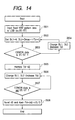
- FIG. 14 is a flowchart that illustrates how the variable delay devices 401, 402 make adjustments. The operation performed to adjust the phase relationship between NRZ and CLK according to the present embodiment will now be described with reference to these drawings.
- a known fixed pattern signal is entered into an NRZ input of the laser driver.
- a 5T-5T pattern is entered.
- the initial delay amounts Tdl1, Tdl2 for the DL1 (401) and DL2 (402) are set so that the delay adjustment amount Td, which is defined in the first embodiment, is 0.
- the microcomputer 204 is used to verify that the signal output from the CDMON is not 5T-5T.
- the area between delay adjustment amounts d2 and d3 represents the NRZ/CLK phase relationship that provides correct NRZ data probing.
- the delay amounts Tdl1, Tdl2 of the DL1 and DL2 are adjusted until the delay adjustment amount Td satisfies the following equation. When the equation is satisfied, the NRZ/CLK phase adjustment is completed.
- the present embodiment produces the same effect as the first to third embodiments of the present invention. Further, unlike the third embodiment, the present embodiment does not require clocks having a frequency that is multiplied by n within the laser driver. Therefore, the present embodiment not only reduces the power consumption required for adjustment but also suppresses the generation of heat. As a result, it makes it possible to avoid PUH case deformation and other problems that may arise from local heat generation by the laser driver within the PUH.
- a fifth embodiment of the present invention will now be described. It is assumed that the configuration of an optical disk apparatus of the fifth embodiment is the same as in the first embodiment, which is illustrated in FIG. 5. It is also assumed that a laser driver 201 outputs NRZ/CLK phase adjustment monitor signal SKMON to a microcomputer 204, which controls delay devices 401, 402.
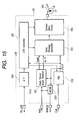
- FIG. 15 shows the configuration of a laser driver 201 according to the fifth embodiment.
- Components having the same functions as the counterparts indicated in FIG. 3 are assigned the same reference numerals as the counterparts in FIG. 3 and their description is omitted herein.
- the laser driver shown in FIG. 15 differs from the one in FIG. 3 in that the former is additionally provided with block MON2, which generates monitor signal SKMON for NRZ/CLK phase adjustment from NRZ and internal clock chCLK.
- FIG. 1 is a circuit diagram that illustrates the above-mentioned MON2 and its peripheral devices.
- the reference numeral 101 in the figure indicates a D flip-flop 101, which generates monitor signal SKMON for NRZ/CLK phase adjustment.
- FIG. 16 is a flowchart that illustrates the NRZ/CLK phase adjustment operation according to the present embodiment. The operation of the present embodiment will now be described with reference to FIG. 16. The present embodiment assumes that NRZ strobing takes place at a rising edge of CLK as is the case with the first embodiment of the present invention.
- the SKMON output is stored (1201) while the delay amounts Tdl1, Tdl2 of the DL1 (401) and DL2 (402), which are defined for the first embodiment, are varied to change the delay adjustment amount Td from 0 to d1 (maximum value).
- the storage result is checked to determine whether the edge count is 0, 1, 2, or 3 (1202-1204). Subsequently control is exercised as appropriate for the determined edge count (1205-1208).
- the flowchart in FIG. 17 illustrates how the delay adjustment amount Td is adjusted. First, a check is performed to determine whether the second edge is rising or falling (1301).
- the DSP 203 achieves synchronization when the NRZ and CLK phases are at a rising edge (in phase with a strobe edge) and the DSP internally assures that an NRZ edge is timed with a delay of fixed time dT3 after a falling edge of CLK.
- a check is performed to determine whether the first edge is rising or falling (1601).
- the flowchart in FIG. 23 illustrates how the delay adjustment amount Td is adjusted. First, a check is performed to determine whether the first edge is rising or falling (1901).
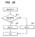
- the flowchart in FIG. 26 illustrates how the delay adjustment amount Td is adjusted.
- the delay adjustment amount is then determined in accordance with the NRZ/CLK edge relationship (2201).
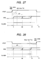
- the range of NRZ edge variation caused by a Td change is positioned after a strobe edge, as indicated in FIG. 27. Therefore, the purpose is achieved when the DL1 and DL2 delay amounts are adjusted until the value Td equals d1 (maximum).
- the range of NRZ edge variation caused by a Td change is positioned before a strobe edge, as indicated in FIG. 28. Therefore, the purpose is achieved when the DL1 and DL2 delay amounts are adjusted until the value Td equals 0 (minimum).
- the present embodiment not only produces the same effect as the first to fourth embodiments but also introduces the following improvements:
- the optimum NRZ edge position can be detected within an adjustment range even when the NRZ phase adjustment range is narrower than one CLK cycle.
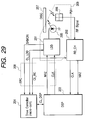
- FIG. 29 illustrates the configuration of an optical disk apparatus according to a sixth embodiment of the present invention.
- Components having the same functions as the counterparts indicated in FIG. 5 are assigned the same reference numerals as the counterparts in FIG. 5 and their description is omitted herein.
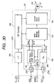
- FIG. 30 shows the configuration of a laser driver 201 according to the present embodiment.
- Components having the same functions as the counterparts indicated in FIG. 15 are assigned the same reference numerals as the counterparts in FIG. 15 and their description is omitted herein.
- variable delay devices DL1 and DL2 for NRZ/CLK phase adjustment which are at a stage preceding the laser driver 201, are incorporated into the laser driver and designated as DL3 and DL4 (2701, 2702), respectively.
- the method for adjusting variable delay devices DL3 and DL4 is the same as for the fifth embodiment.
- the present embodiment produces the same effect as the fifth embodiment and uses a smaller number of optical disk apparatus components than the fifth embodiment. Therefore, the present embodiment contributes toward equipment downsizing and cost reduction.
- the present embodiment may use the same method as the fifth embodiment, but produces the same effect even when it uses the same DL3/DL4 adjustment method as the first to fourth embodiments.
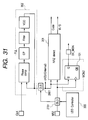
- FIG. 31 is a circuit diagram, which illustrates a PLL in the laser driver and a mark/space detector block according a seventh embodiment of the present invention.
- the present embodiment is equal to the sixth embodiment in optical disk apparatus configuration and laser driver configuration.
- the difference between the present embodiment and the sixth embodiment is that the former eliminates variable delay device DL4 (2702) for CLK phase adjustment and furnishes variable delay device DL5 (2801) for phase adjustment to the PLL output of internal clock chCLK, which is synchronized with CLK by the PLL 302.
- the method for adjusting variable delay devices DL3 and DL4 is the same as with the fifth embodiment.
- the present embodiment produces the same effect as the sixth embodiment. Since an internal clock generally provides a higher degree of duty cycle stability than an external clock, the configuration of the present embodiment offers a higher degree of CLK/NRZ phase adjustment accuracy than that of the fifth embodiment. As a result, an increased margin can be provided for a phase shift between NRZ and CLK.
- the present embodiment may use the same method as the fifth embodiment, but produces the same effect even when it uses the same DL3/DL4 adjustment method as the first to fourth embodiments.
- FIG. 32 shows a block diagram of a laser driver according to an eighth embodiment of the present invention.
- Components having the same functions as the counterparts indicated in FIG. 30, which describes the sixth embodiment, are assigned the same reference numerals as the counterparts in FIG. 30 and their description is omitted herein.
- the configuration of the optical disk apparatus according to the eighth embodiment is similar to the configuration shown in FIG. 29 except that the former is without monitor signal SKMON, which the laser driver 201 transmits to the microcomputer 204.
- the difference between FIG. 29 and FIG. 32 is as follows:
- the same delay amount adjustment sequence is followed by the delay circuits 2701, 2702 as in the fifth embodiment.
- the present embodiment produces the same effect as the fifth embodiment.
- the present embodiment requires fewer connection lines between the laser driver 201 and the microcomputer 204 for controlling the laser driver and uses a smaller number of FPC wiring lines than the fourth embodiment.
- the present embodiment requires a shorter period of control time than the fourth embodiment because the microcomputer and other components are not involved in adjustment.
- the present embodiment may use the same method as the fifth embodiment, but produces the same effect even when it uses the same DL3/DL4 adjustment method as the first to fourth and seventh embodiments.
- the present embodiment may adopt the same variable delay device insertion position as the sixth embodiment, but produces the same effect even when it uses the same variable delay device insertion position as the eighth embodiment.
- the same effect can be produced even when either of the NRZ or CLK signal is subjected to phase adjustment by the variable delay circuits.
- the NRZ signal is used as an example of a binary signal.
- an NRZI or other signal may be used as the binary signal for the present invention.
- the present invention relates to an optical disk apparatus's laser driver having means for generating a recording waveform, known as a recording strategy, from a recording clock signal and the modulated signal to be recorded, and makes it possible to adjust the phases of a recording clock signal and modulated signal transmitted from a DSP or other means for modulated signal generation in order to reduce the possibility of recording strategy generation error, which may result from an improper phase relationship between the two signals.
- a recording strategy known as a recording strategy
Landscapes
- Engineering & Computer Science (AREA)
- Signal Processing (AREA)
- Optical Recording Or Reproduction (AREA)
- Optical Head (AREA)
- Signal Processing For Digital Recording And Reproducing (AREA)
Abstract
Description
Claims (12)
- An optical disk apparatus equipped with a laser driver for generating a drive waveform that drives a laser diode in accordance with the binary recording signal and recording clock signal to be recorded on a recording medium, the optical disk apparatus comprising:wherein the delay amounts provided by said two delay circuits are varied to adjust the relative timing between the edges of said binary recording signal and recording clock signal.a binary recording signal delay circuit for performing a delay process on said binary recording signal in accordance with a control signal; anda recording clock signal delay circuit for performing a delay process on said recording clock signal in accordance with the control signal,
- The optical disk apparatus according to claim 1, wherein said delay circuits are incorporated in said laser driver.
- An optical disk apparatus equipped with a laser driver for generating a drive waveform that drives a laser diode in accordance with the binary recording signal and recording clock signal to be recorded on a recording medium,
wherein said laser driver comprises:wherein the delay amount provided by said internal clock output delay circuit is varied to adjust the relative timing between the edges of said binary recording signal and recording clock signal.phase synchronization means for synchronizing the phase of the recording clock signal to be entered into said laser driver and the phase of an internal clock signal of said laser driver; andan internal clock output delay circuit which is provided after an internal clock output of said phase synchronization means, and - The optical disk apparatus according to claim 3, further comprising:wherein the delay amounts provided by said two delay circuits are varied to adjust the relative timing between the edges of said binary recording signal and recording clock signal.a binary recording signal delay circuit for performing a delay process on said binary recording signal, and
- The optical disk apparatus according to claim 4, wherein a logic inverter circuit is provided before said recording clock signal delay circuit.
- A phase adjustment method used in accordance with an entered binary signal and clock signal when the value of said binary signal is detected, the method comprising:wherein said delay processes detect a binary signal while varying the delay amounts for the binary recording signal and recording clock signal, compare an entered known binary signal against the detected binary signal, and adjust the delay amounts to be applied to the binary recording signal and recording clock signal.a binary recording signal delay process for performing a delay process on said binary recording signal in accordance with a control signal; anda recording clock signal delay process for performing a delay process on said recording clock signal in accordance with the control signal,
- A phase adjustment method for adjusting the phase relationship between a modulated signal and a recording clock signal within an optical disk apparatus equipped with a laser driver for generating a drive waveform that drives a laser diode in accordance with the binary recording signal and recording clock signal to be recorded on a recording medium, the method comprising the steps of:wherein the latter step is performed, while varying the delay amounts provided by said variable delay circuits, to detect a delay amount change term of said delay circuits during which the information difference is approximately zero, and employ values prevailing during said detected delay amount change term as the delay amounts of the delay circuits.entering a known binary recording signal into said laser driver to record it on a recording medium while varying the delay amounts to be applied to said binary signal or recording clock signal; anddetecting the information difference between a playback signal, which is obtained by playing back said recorded signal on said optical disk apparatus, and said binary recording signal,
- A phase adjustment method for adjusting the phase relationship between a modulated signal and a recording clock signal within an optical disk apparatus equipped with a laser driver for generating a drive waveform that drives a laser diode in accordance with the binary recording signal and recording clock signal to be recorded on a recording medium, the method comprising the steps of:measuring the phase difference between an edge in opposite phase with a recording clock signal edge for strobing a binary recording signal in said laser driver and a binary recording signal edge while varying the delay amount to be applied to said binary signal or recording clock signal;detecting a delay amount change term of said variable delay circuits during which the phase difference is approximately zero; andemploying values prevailing during said detected delay amount change term as the delay amounts of the variable delay circuits.
- The phase adjustment method for adjusting the phase relationship between a modulated signal and a recording clock signal according to claim 8, wherein a signal having a higher frequency than that of a recording clock signal is generated within said laser driver to measure said phase difference in accordance with the generated signal.
- A phase adjustment method for adjusting the phase relationship between a modulated signal and a recording clock signal within an optical disk apparatus equipped with a laser driver for generating a drive waveform that drives a laser diode in accordance with the binary recording signal and recording clock signal to be recorded on a recording medium, the method comprising the steps of:entering a known binary recording signal into said laser driver while varying the delay amount to be applied to said binary signal or recording clock signal;detecting a delay amount change term of said variable delay circuits during which approximately zero information difference exists between a signal obtained by latching a binary recording signal entered in the laser driver with a recording clock signal and said known binary recording signal; andemploying values prevailing during said detected delay amount change term as the delay amounts of the delay circuits.
- A phase adjustment method for adjusting the phase relationship between a modulated signal and a recording clock signal within an optical disk apparatus equipped with a laser driver for generating a drive waveform that drives a laser diode in accordance with the binary recording signal and recording clock signal to be recorded on a recording medium, wherein the method detects said variable delay circuits' delay amounts prevailing when the timing of a binary recording signal edge is in approximate agreement with or closest to the timing of an edge in opposite phase with a recording clock signal edge for strobing a modulated signal in said laser driver, in accordance with the signal change and signal polarity obtained by latching a recording clock signal entered in said laser driver with a binary recording signal entered in the laser driver, while varying the delay amount to be applied to said binary signal or recording clock signal, and employs said detected delay amount values as the delay amounts of the variable delay circuits.
- A laser driver for generating a drive waveform that drives a laser diode in accordance with the binary recording signal and recording clock signal to be recorded on a recording medium, the laser driver comprising:wherein either or both of the delay amounts of said two delay circuits are varied in accordance with said control signal to adjust the relative timing between the edges of said binary recording signal and recording clock signal.a binary recording signal delay circuit for performing a delay process on said binary recording signal;a recording clock signal delay circuit for performing a delay process on said recording clock signal; andinput means for entering a control signal that controls the delay amount of said binary recording signal delay circuit or recording clock signal delay circuit,
Applications Claiming Priority (2)
| Application Number | Priority Date | Filing Date | Title |
|---|---|---|---|
| JP2002313623A JP3931133B2 (en) | 2002-10-29 | 2002-10-29 | Optical disc apparatus and phase adjustment method |
| JP2002313623 | 2002-10-29 |
Publications (3)
| Publication Number | Publication Date |
|---|---|
| EP1416487A2 true EP1416487A2 (en) | 2004-05-06 |
| EP1416487A3 EP1416487A3 (en) | 2005-04-27 |
| EP1416487B1 EP1416487B1 (en) | 2007-10-10 |
Family
ID=32089485
Family Applications (1)
| Application Number | Title | Priority Date | Filing Date |
|---|---|---|---|
| EP03254643A Expired - Lifetime EP1416487B1 (en) | 2002-10-29 | 2003-07-25 | Optical disk apparatus and phase adjustment method |
Country Status (6)
| Country | Link |
|---|---|
| US (1) | US20040136286A1 (en) |
| EP (1) | EP1416487B1 (en) |
| JP (1) | JP3931133B2 (en) |
| KR (1) | KR100562452B1 (en) |
| CN (1) | CN1314013C (en) |
| DE (1) | DE60316760T2 (en) |
Families Citing this family (7)
| Publication number | Priority date | Publication date | Assignee | Title |
|---|---|---|---|---|
| DE10126802C2 (en) * | 2001-06-01 | 2003-05-08 | Texas Instruments Deutschland | Method for the transmission of data via a bus and bus system for carrying out the method |
| JP4310256B2 (en) | 2004-10-22 | 2009-08-05 | 株式会社日立製作所 | Optical disc recording apparatus, laser diode driving apparatus, and recording signal generating apparatus |
| US7394747B2 (en) * | 2004-11-02 | 2008-07-01 | Mediatek Incorporation | Optical storage system having integrated laser driver signal processor |
| JP2007073147A (en) * | 2005-09-08 | 2007-03-22 | Hitachi Ltd | Optical disk device and integrated circuit used therefor |
| WO2007052178A2 (en) * | 2005-10-31 | 2007-05-10 | Koninklijke Philips Electronics N.V. | An optical drive having a laser driver device with an adjustable power level |
| US8089842B2 (en) * | 2006-05-25 | 2012-01-03 | Mediatek Inc. | System and method for controlling data recording process of optical recording medium in sequential writing |
| JP2009080928A (en) * | 2008-11-26 | 2009-04-16 | Hitachi Ltd | Optical disc recording apparatus, laser diode driving apparatus, and recording signal generating apparatus |
Family Cites Families (8)
| Publication number | Priority date | Publication date | Assignee | Title |
|---|---|---|---|---|
| JPH08227560A (en) * | 1995-02-21 | 1996-09-03 | Sony Corp | Digital signal recording / reproducing apparatus and method |
| EP0969452A4 (en) * | 1997-03-25 | 2000-12-27 | Sanyo Electric Co | Information reproducer, information recorder and reference mark detection circuit |
| JPH1166591A (en) * | 1997-08-22 | 1999-03-09 | Sharp Corp | Semiconductor laser drive signal generation circuit and optical recording / reproducing apparatus provided with this semiconductor laser drive signal generation circuit |
| JPH11213429A (en) * | 1998-01-30 | 1999-08-06 | Sony Corp | Recording device and recording method for phase change optical disk |
| US6721255B1 (en) * | 1998-10-28 | 2004-04-13 | Matsushita Electric Industrial Co., Ltd. | Device and method for recording data to optical disk using recording pulse with corrected edge position |
| JP3528692B2 (en) * | 1999-07-30 | 2004-05-17 | 株式会社日立製作所 | Information recording / reproducing device, laser driver, and driving method of laser driver |
| JP2001202625A (en) * | 2000-01-17 | 2001-07-27 | Toshiba Corp | Data recording signal generator for optical disk |
| JP3740413B2 (en) * | 2001-12-20 | 2006-02-01 | 株式会社日立製作所 | High frequency superimposing method and optical disk apparatus using the same |
-
2002
- 2002-10-29 JP JP2002313623A patent/JP3931133B2/en not_active Expired - Fee Related
-
2003
- 2003-07-25 DE DE60316760T patent/DE60316760T2/en not_active Expired - Fee Related
- 2003-07-25 EP EP03254643A patent/EP1416487B1/en not_active Expired - Lifetime
- 2003-07-29 KR KR1020030052303A patent/KR100562452B1/en not_active Expired - Fee Related
- 2003-07-30 CN CNB031522947A patent/CN1314013C/en not_active Expired - Fee Related
- 2003-07-30 US US10/631,575 patent/US20040136286A1/en not_active Abandoned
Also Published As
| Publication number | Publication date |
|---|---|
| KR100562452B1 (en) | 2006-03-20 |
| KR20040038604A (en) | 2004-05-08 |
| JP3931133B2 (en) | 2007-06-13 |
| US20040136286A1 (en) | 2004-07-15 |
| DE60316760D1 (en) | 2007-11-22 |
| EP1416487A3 (en) | 2005-04-27 |
| CN1494066A (en) | 2004-05-05 |
| DE60316760T2 (en) | 2008-07-17 |
| EP1416487B1 (en) | 2007-10-10 |
| JP2004152335A (en) | 2004-05-27 |
| CN1314013C (en) | 2007-05-02 |
Similar Documents
| Publication | Publication Date | Title |
|---|---|---|
| US7453658B2 (en) | Recording control apparatus, recording and reproduction apparatus, and recording control method | |
| US7200091B2 (en) | Light source driving unit and optical storage apparatus | |
| KR19980081394A (en) | Optical Disc Device | |
| EP1416487B1 (en) | Optical disk apparatus and phase adjustment method | |
| US20010038586A1 (en) | Optical information recording apparatus for stable recording | |
| JP3836313B2 (en) | Optical recording method and optical recording apparatus | |
| US20070242584A1 (en) | Dynamic write strategy modification method and apparatus | |
| JP4185811B2 (en) | Laser-driven integrated circuit and optical disk apparatus | |
| US7274643B2 (en) | Information recording and reproducing apparatus and information recording medium | |
| US9030922B2 (en) | Method and apparatus for laser control during recording | |
| EP0871171A2 (en) | Signal converting device and information recording apparatus employing the same | |
| JP2002208144A (en) | Optical disk and optical disk reproducing device | |
| KR100731245B1 (en) | Optical disc apparatus and optical disc evaluating method | |
| US7200081B2 (en) | Write strategy circuit, write strategy method, and optical disk apparatus | |
| JP2003173535A (en) | Optical disk recording / reproducing apparatus and optical disk recording method | |
| US20060285467A1 (en) | Optical disk apparatus and method of evaluating optical disks | |
| US20040145990A1 (en) | Writable area detection device for optical recording/reproducing apparatus and method thereof | |
| KR100808034B1 (en) | Disk reproducing apparatus and method | |
| JP2002312938A (en) | Optical disk recorder | |
| JPH1055543A (en) | Optical information reproducing device | |
| JP2004246934A (en) | Optical disk recording device | |
| JP2006344339A (en) | Optical recording medium recording / reproducing apparatus and recording parameter correction method thereof |
Legal Events
| Date | Code | Title | Description |
|---|---|---|---|
| PUAI | Public reference made under article 153(3) epc to a published international application that has entered the european phase |
Free format text: ORIGINAL CODE: 0009012 |
|
| 17P | Request for examination filed |
Effective date: 20030818 |
|
| AK | Designated contracting states |
Kind code of ref document: A2 Designated state(s): AT BE BG CH CY CZ DE DK EE ES FI FR GB GR HU IE IT LI LU MC NL PT RO SE SI SK TR |
|
| AX | Request for extension of the european patent |
Extension state: AL LT LV MK |
|
| PUAL | Search report despatched |
Free format text: ORIGINAL CODE: 0009013 |
|
| AK | Designated contracting states |
Kind code of ref document: A3 Designated state(s): AT BE BG CH CY CZ DE DK EE ES FI FR GB GR HU IE IT LI LU MC NL PT RO SE SI SK TR |
|
| AX | Request for extension of the european patent |
Extension state: AL LT LV MK |
|
| RIC1 | Information provided on ipc code assigned before grant |
Ipc: 7G 11B 7/0045 B Ipc: 7G 11B 7/125 B Ipc: 7G 11B 20/10 A |
|
| AKX | Designation fees paid |
Designated state(s): DE FR GB |
|
| 17Q | First examination report despatched |
Effective date: 20051027 |
|
| GRAP | Despatch of communication of intention to grant a patent |
Free format text: ORIGINAL CODE: EPIDOSNIGR1 |
|
| GRAS | Grant fee paid |
Free format text: ORIGINAL CODE: EPIDOSNIGR3 |
|
| GRAA | (expected) grant |
Free format text: ORIGINAL CODE: 0009210 |
|
| AK | Designated contracting states |
Kind code of ref document: B1 Designated state(s): DE FR GB |
|
| REG | Reference to a national code |
Ref country code: GB Ref legal event code: FG4D |
|
| REF | Corresponds to: |
Ref document number: 60316760 Country of ref document: DE Date of ref document: 20071122 Kind code of ref document: P |
|
| ET | Fr: translation filed | ||
| PLBE | No opposition filed within time limit |
Free format text: ORIGINAL CODE: 0009261 |
|
| STAA | Information on the status of an ep patent application or granted ep patent |
Free format text: STATUS: NO OPPOSITION FILED WITHIN TIME LIMIT |
|
| 26N | No opposition filed |
Effective date: 20080711 |
|
| PGFP | Annual fee paid to national office [announced via postgrant information from national office to epo] |
Ref country code: FR Payment date: 20080627 Year of fee payment: 6 |
|
| PGFP | Annual fee paid to national office [announced via postgrant information from national office to epo] |
Ref country code: GB Payment date: 20080620 Year of fee payment: 6 |
|
| PGFP | Annual fee paid to national office [announced via postgrant information from national office to epo] |
Ref country code: DE Payment date: 20080924 Year of fee payment: 6 |
|
| GBPC | Gb: european patent ceased through non-payment of renewal fee |
Effective date: 20090725 |
|
| REG | Reference to a national code |
Ref country code: FR Ref legal event code: ST Effective date: 20100331 |
|
| PG25 | Lapsed in a contracting state [announced via postgrant information from national office to epo] |
Ref country code: FR Free format text: LAPSE BECAUSE OF NON-PAYMENT OF DUE FEES Effective date: 20090731 |
|
| PG25 | Lapsed in a contracting state [announced via postgrant information from national office to epo] |
Ref country code: GB Free format text: LAPSE BECAUSE OF NON-PAYMENT OF DUE FEES Effective date: 20090725 |
|
| PG25 | Lapsed in a contracting state [announced via postgrant information from national office to epo] |
Ref country code: DE Free format text: LAPSE BECAUSE OF NON-PAYMENT OF DUE FEES Effective date: 20100202 |