EP1416367A2 - Electromagnetic coordinate input system, electromagnetic coordinate input method and pointer device - Google Patents
Electromagnetic coordinate input system, electromagnetic coordinate input method and pointer device Download PDFInfo
- Publication number
- EP1416367A2 EP1416367A2 EP03254582A EP03254582A EP1416367A2 EP 1416367 A2 EP1416367 A2 EP 1416367A2 EP 03254582 A EP03254582 A EP 03254582A EP 03254582 A EP03254582 A EP 03254582A EP 1416367 A2 EP1416367 A2 EP 1416367A2
- Authority
- EP
- European Patent Office
- Prior art keywords
- inductive
- loop
- electromagnetic
- physical
- circuit
- Prior art date
- Legal status (The legal status is an assumption and is not a legal conclusion. Google has not performed a legal analysis and makes no representation as to the accuracy of the status listed.)
- Granted
Links
Images




Classifications
-
- G—PHYSICS
- G06—COMPUTING OR CALCULATING; COUNTING
- G06F—ELECTRIC DIGITAL DATA PROCESSING
- G06F3/00—Input arrangements for transferring data to be processed into a form capable of being handled by the computer; Output arrangements for transferring data from processing unit to output unit, e.g. interface arrangements
- G06F3/01—Input arrangements or combined input and output arrangements for interaction between user and computer
- G06F3/03—Arrangements for converting the position or the displacement of a member into a coded form
- G06F3/041—Digitisers, e.g. for touch screens or touch pads, characterised by the transducing means
- G06F3/046—Digitisers, e.g. for touch screens or touch pads, characterised by the transducing means by electromagnetic means
Definitions
- the present invention generally relates to a multi-induction loop layout of an electromagnetic inductive system, and more particularly to a method for locating the coordinates of the multi-induction loop layout of an electromagnetic inductive system.
- a handwriting input device can replace a mouse and allow users to input words and pictures by hand, more easily than a mouse, the field of improvement of a handwriting input device has developed rapidly in recent years.
- the early handwriting input device replaces a mouse with a pen.
- a cordless pointer device such as a pen, a mouse, a puck or a stylus with a digitizer tablet is usually used.
- the tip of the cordless pen or stylus corresponds with the left key of the mouse.
- conventional pen-input products have existed for several years, similar kinds of products generally focus on the application of a single function such as graphing, drawing or Chinese text key-in.
- the conventional electromagnetic inductive system is equipped with a digitizer tablet and a mouse or pen-transducer/pointer device.
- the mechanical or optical type mouse device generally functions in the relative mode, that is to say , when the mouse glides on the surface of the mouse pad, the computer system receives the cursor information from the mouse and it can only identify the relative movement in X and Y directions.
- a common technique is to implement a pair of mutually perpendicular altering signals in the mouse, these two signals corresponding to the longitudinal and transverse movement of the mouse.
- the cursor device of the tablet such as cordless pointer device, generally functions in the absolute mode.
- the signal changes in order to response the new absolute coordinates of the pointer device.
- the electromagnetic field inductive technique is the technique that generally applies to the absolute mode.
- the early transducer/pointer devices were connected to the tablet with a set of wires, delivering the information of coordinates and switch/pressure status to the computer system with interface.
- Some cordless transducers/pointer devices in the prior art indicated the use of different functions by changing the frequency and/or phase, the functions included, pressing down the button, pressing the tip of the pointer device on the active area, and other similar functions.
- the current pointer/input product is usually an electromagnetic inductive system.
- the electromagnetic inductive system usually comprises an electromagnetic pointer device and a tablet.
- the electromagnetic pointer device has an oscillation circuit and a battery, providing energy for transmitting the relative electromagnetic signal. Take the electromagnetic pointer device for example, when the tip of the pointer device is pressed, the inductance of the inductor changes, therefore the oscillation frequency also changes. The higher the pressure received by the pointer device , the greater the inductance changes, and the oscillation frequency, therefore the amount of the pressure exerted upon the pointer device tip of the can be obtained through the changing degree of frequency.
- the tablet also comprises elements such as a detective loop, an amplifier, and an ADC and so on.
- the central writing area of this conventional handwriting tablet is plaited by inductive loops, the layout is composed of double layers of a PCB and the inductive loops with two axial arranged in an array of equal distance. The major use of these inductive loops is to induce the electromagnetic signal transmitted by the electromagnetic pointer device. When the electromagnetic pointer device transmits the electromagnetic signal, these inductive loops will induce the electromagnetic signal and the microprocessor will receive the processed information of the pointer device through a signal processing circuit.
- the inductive loops of the conventional electromagnetic inductive device and its layout design makes the inductive loops a grid net with the X and Y axis arranged in an array at equal distance in order to induce the signal emitted from the electromagnetic pointer device and figure out its absolute coordinates.
- the inductive loops layout deployed according to the X direction of a two-dimensional orthogonal coordinate indicated in FIG. 1A.
- One terminal of each antenna loop 110A is connected respectively with one switch (from X1 to X25).
- the other terminal is connected with the common ground node 105A, through which, the signal induced by each antenna loop 110A can be obtained by controlling the switches X1 to X25 in order.
- the intensity of the magnetic field is an inverse proportion to the square of distance, the farther the distance between the electromagnetic pointer device that's transmitting the electromagnetic field and the inductive loops, the weaker is the signal induced by the inductive loops; in contrast, the nearer the distance between the electromagnetic pointer device that's transmitting the electromagnetic field and the inductive loops , the stronger is the signal induced by the inductive loops. Therefore, as long as the microprocessor of the tablet can scan through all the inductive loops one by one in sequence, and analyze the strength of the signals induced by each inductive loop, the inductive loops in which dominates the range the electromagnetic pointer device located can be identified. The coordinates of its position can be figured out. However, as far as a tablet of a larger size is concerned, the number of inductive loops arranged also increases, and therefore more loop switches are needed.
- the present invention provides a multi-induction loop layout of the electromagnetic inductive system preferably to reduce or eliminate the defect mentioned above.
- the present invention provides a multi-induction loop layout of an electromagnetic inductive system with a battery-less pointer device (a pen, a mouse, a locating plate, etc.) and its method for calculating the coordinates, which is preferably able to reduce or eliminate the said defect of the conventional electromagnetic inductive system.
- One main preferred purpose of the invention is to provide an electromagnetic inductive system with a battery-less pointer device and the multi-induction loops layout and its method for calculating the coordinates.
- the invention preferably processes a procedure of calculating the coordinates through a battery-less pointer device and a multi-induction loop layout.
- the battery-less pointer device of the invention is consisted of a variable inductance element. When the inductance changes, the resonant frequency also changes, and therefore the frequency of the electromagnetic signal induced by the inductive loops also different.
- the invention can reduce the space demand of the electromagnetic inductive system and the size of its PCB (whether it is a inflexible or flexible PCB is not confined here).
- the goal of minimizing the space bounded and the product appearance, reducing production costs, and intensifying the efficiency of the electromagnetic inductive system may be achieved. Therefore, the invention fits in with economic benefit and industrial practicability.
- the multi-induction loop layout of the invention may comprises a multi-induction loop group deployed according to a inductive loop deployment table.
- the inductive loop layout in the inductive loop deployment table may comprise a plurality of physical inductive loops that are distributed along the X and Y axis of the two-dimensional orthogonal coordinates system and each physical inductive loop comprises a plurality of logical inductive loops.
- the logical inductive loops that are adjacent to the two sides of each logical inductive loop may belong to a different physical inductive loop.
- each loop switch is switched on its physical inductive loop in sequence in a specific time slot to transmit an electromagnetic signal.
- the battery-less pointer device When the battery-less pointer device is in the region of the multi-induction loop layout, it induces the electromagnetic energy transmitted by the physical inductive loop.
- the bi-direction loop switch of the physical inductive loop may stop transmitting energy and start to induce the energy transmitted by the battery-less pointer device.
- the positioning procedure of the battery-less pointer device of the electromagnetic inductive system includes, ⁇ Full Scan ⁇ and its ⁇ Partial Scan ⁇ procedure of X and Y direction in order to detect the first signal, possessing the highest voltage, the second signal, possessing the voltage second to the highest, and the third signal, possessing the third highest voltage orderly and figure out the accurate coordinates of the battery-less pointer device through the calculation of the internal circuit processing and microprocessor of the electromagnetic inductive system.
- the invention provides an electromagnetic inductive system, as set out in claim 1.
- the invention provides a method for finding the coordinates of an electromagnetic inductive system, as set out in claim 6.
- a multi-induction loop 200 is provided, one end of which being electrically coupled with a loop switch 210, and the other end of which being electrically coupled with a common node 220.
- the multi-induction loop 200 comprises a plurality of -type sections.
- the a plurality of -type sections 230A to 230C are composed of the first sawtooth-shaped region 260A.
- the a plurality of -type sections 240A to 240C are composed of a second sawtooth-shaped region 260B.
- the second sawtooth-shaped region 260B and the first sawtooth-shaped region 260A make up a relative close inductive loop.
- the multi-induction loop is a physical inductive loop.
- the conducting wire loop forming the close-like regions 250A, 250B, and 250C are a plurality of logical inductive loops, that is to say, a physical inductive loop will include a plurality of logical inductive loops. This is the reason why the present technique is called "multi-induction loop".
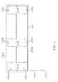
- a multi-induction loop layout 300 (only the x axis of which is indicated) with a plurality of physical inductive loops (X1-X9 and XA-XC) is provided.
- Each physical inductive loop (from X1 to X9 and from XA to XC) is being deployed along the X axis of the orthogonal two-dimensional coordinates and composed by a plurality of logical inductive loops 310, which are essentially consistent -type sections.
- Each multi-induction loop (from X1 to X9 and from XA to XC) is electrically coupled with a corresponding loop switch 330, and the other terminal of the loop is electrically coupled with a common node 320.
- each logical inductive loop 310 and other adjacent logical inductive loops specifically correspond to a respective physical inductive loop (X1-X9 and XA-XC). Therefore, a specific logical inductive loop on which the pointer device is located within the inductive loop can be identified.
- a -type logical inductive loop 310A of the physical inductive loop X5 for example, the logical inductive loops adjacent to it, 310C and 310D, respectively belong to physical inductive loops X4 and X6.
- the pointer device is located on the -type section 310A or 310B of the physical inductive loop X5, can be differentiated by referring to the inductive signal voltage produced by the physical inductive loops X4, X6, X2, and X12, to which the physical inductive loop X5 and the logical inductive loops adjacent to it correspond.
- the distance between the two adjacent logical inductive loops of the same physical inductive loop must be kept at an appropriate distance. For example, misjudgment in locating the pointer device occurs if the distance "L" is too short between the two adjacent - type logical inductive loops 310A and 310B of the physical inductive loop X5.
- an electromagnetic inductive system 400A is provided.
- the pointer device which is a battery-less pointer device 400B, has an electromagnetic inductive storage circuit that comprises a variable inductor.
- the electromagnetic inductive system 400A comprises a set of loops sub-circuit 405, an interior circuit 410, and a microprocessor sub-circuit 415.
- the interior circuit 410 comprising a filter and amplifier sub-circuit 420, a pre-amplifier sub-circuit 425, a waveform generating sub-circuit 430, and a frequency-to-voltage converter sub-circuit 435, and the loops sub-circuit 405 comprising a multi-inductive loop layout 440 and a group of the loop switches 445.
- the multi-inductive loop layout 440 comprises a plurality of physical inductive loops 450 that are electrically coupled respectively with a plurality of bi-direction loop switches 445A of the loop switch group 445, which is electrically coupled with the pre-amplifier sub-circuit 425 and controlled by a microprocessor sub-circuit 415.
- the pre-amplifier sub-circuit 425 is also electrically coupled with the filter and the amplifier sub-circuit 420 and controlled by the microprocessor sub-circuit 415.
- the filter and amplifier sub-circuit 420 is electrically coupled respectively with the waveform generating sub-circuit 430 and the frequency-to-voltage converter sub-circuit 435.
- the waveform generating sub-circuit 430 and the frequency-to-voltage converter sub-circuit 435 is electrically coupled with the microprocessor sub-circuit 415 respectively.
- a signal After a signal is received by the a plurality of physical inductive loops 450 , it's transmitted to, and amplified by the pre-amplifier sub-circuit 425, before being transmitted to the filter and amplifier sub-circuit 420, in order to filter out the noise signals of unnecessary frequency bands, and the signal is also amplified again, then transmitted to the waveform generating sub-circuit 430 and frequency-to-voltage converter sub-circuit 435 to produce a specific signal waveform and convert the signal frequency into a voltage signal. Finally to be transmitted respectively to the microprocessor sub-circuit 415 to proceed with the differentiation in the coordinates operation and non-position signal.
- the a plurality of physical inductive loops 450A and 450B of the multi-induction loop layout 440 are deployed in the direction of the X axis and Y axis of the two-dimension orthogonal coordinates.
- One terminal of all physical inductive loops 450A and 450B is electrically coupled with the same common node 455.
- the other terminal of all physical inductive loops 450A and 450B is electrically coupled with a plurality of bi-direction loop switch 445A of the loop switch group 445.
- the a plurality of physical inductive loops 450A and 450B being composed by a connection of essentially consistent a plurality of -type sections.
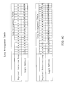
- the multi-induction loop layout 440 is indicated in an inductive loop deployment table in FIG.4C.
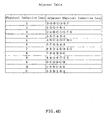
- the inductive loop deployment table (as FIG.4C indicates) being built in the microprocessor sub-circuit 415 and containing an adjacency table (as FIG.4C indicates) that indicates the adjacency relation between different physical inductive loops 450A and 450B and their corresponding logical inductive loops.
- There is a physical address for the position of each physical inductive loop from X1 to X9 and from XA to XC
- there is a logical address (from 1 to 41) for the position of each logical inductive loop.
- the physical inductive loops of the adjacent logical inductive loops are not repeated.
- the physical inductive loop XC for example, its logical inductive loops are 13, 14, and 15, belonging respectively to physical inductive loops X3, XC, and X5, and the logical inductive loops of another section that belong to the same physical inductive loop XC are 23, 24, and 25.
- the electromagnetic inductive system 400A can locate its battery-less pointer device 400B by its inductive loop deployment table.
- the method for detecting the battery-less pointer device 400B is described as follows. First, after the electromagnetic inductive system 400A is started, the loop switch group 445 selects a signal according to the switch transmitted by the microprocessor sub-circuit 415, sets the bi-direction loop switch 445A on/off for each physical inductive loop 450A and 450B in the X direction and Y direction, one by one orderly according to time, and proceeds a ⁇ Full-Scan ⁇ procedure.
- the method of which is that the physical inductive loop transmits an electromagnetic signal, which is induced and received by the battery-less pointer device 400B when the battery-less pointer device 400B approaches the multi-induction loop layout 440.
- the duration of switching on the bi-direction loop switch 445A determined by the default value of the microprocessor sub-circuit 415, which must be long enough for the energy storage of the battery-less pointer device to store energy fully.
- the battery-less pointer device transmits another electromagnetic signal to the a plurality of physical inductive loops that are on its location.
- a ⁇ Full Scan ⁇ procedure is performed first to roughly find the logical address of the pointer device, and then the partial scan is proceeded according to this rough logical address.
- the so-called " ⁇ Full Scan ⁇ procedure" mentioned above is: first, in the first time slot of the scan process, the transmitting circuit is electrically connected with the physical inductive loop by switching the loop switch "ON", to which the first physical inductive loop corresponds. In this time slot, an electromagnetic signal is transmitted into the adjacent space. Second, in another time slot, the transmitting of an electromagnetic signal stops and the loop switch is not switched "OFF". The electromagnetic field of the adjacent space is induced and received by the inductive loop at the same time.
- a value relative to the intensity of the inductive signal is figured out through the process and the operation of the pre-amplifier circuit 425, the filter and amplifier circuit 420, and the microprocessor sub-circuit 415, etc.
- the record of which is set in the RAM(random access memory) of the microprocessor sub-circuit 415; then, the procedure mentioned above is proceeded again with the second physical inductive loop as its object of function. Then, the values relative to the intensity of the inductive signal are compared and the relation between them is recorded. The same procedure is repeated until it has been deployed in all the physical inductive loops.
- a maximum is searched in the records, if there is a maximum, the correspondence is proceeded according to the inductive loop deployment table and the ⁇ Partial Scan ⁇ is ready to proceed after several relative physical inductive loops are found. If there is not a maximum, the " ⁇ Full Scan ⁇ procedure" mentioned above is repeated until there is a maximum.
- the electromagnetic signal is transmitted to an adjacent place.
- the physical inductive loop to which the logical inductive loop with the maximum and its adjacent a plurality of logical inductive loops (including the logical inductive loop with the maximum) correspond, induces and receives the signals, and records the value of each in the microprocessor sub-circuit 415.
- the signals are then arranged to find the strongest, the second strongest, and the third strongest, etc. These are called, the first signal, second signal, and the third signal, etc.
- the voltage of the first signal should be higher than or equal to that of the second signal, and the voltage of the second signal should be higher than or equal to that of the third signal.
- the accurate coordinates are figured out according to these three signals with the linear relationship, and the track of the pointer device is traced by comparing the physical inductive loop with the maximum to see whether it changes or not.
- the microprocessor sub-circuit 415 traces and identifies the logical address of the battery-less pointer device and figures out its coordinates through five voltage signals and the inductive loop deployment table.
- inductive signals of the three highest voltages have a feature that the second strongest signal and the third strongest signal are located on two sides of the first strongest signal. Therefore, it can be clearly known that battery less pointer device is located on the side where the strongest signal is located of physical antenna loop by identifying adjacent locations of physical antenna loop where the second strongest signal locates and physical antenna loop where the first strongest signal locates according to loop deployment table shown in FIG.4C, and the precise address of battery less pointer device can be achieved more rapidly through calculating the first and second strongest signals by microprocessor sub-circuit 415.
- each physical inductive loop can form a -type inductive loop after a circling of a plurality of, and therefore can intensify the first electromagnetic signal transmitted by the physical inductive loop and greatly increase the energy storage efficiency of the battery-less pointer device, thus intensifying the second electromagnetic signal transmitted, and reducing the time for energy storage.
- This enhances the ability of the second electromagnetic signal received by the physical inductive loop at the same time. Therefore, the -type logical inductive loop is formed after the a plurality of is transmitted through each physical inductive loop, which intensifies the voltage signal of the present multi-induction loop layout.
- the tablet of the invention can greatly enhance the stability of the system with its excellent S/N ratio.
- the number of the physical inductive loops of the embodiment of the present invention is not limited to 12 loops, the design of which, varying according to practical application.
- the battery-less pointer device of the present invention possesses a variable inductance element, when the inductance of which changes, the resonant frequency also changes, thus the frequency of the electromagnetic signal transmitted by the battery-less pointer device that is induced by the inductive loop also varies.
- the invention can reduce space demand of the electromagnetic inductive system and the size of its PCB (whether it is inflexible type or flexible type is not limited) to achieve the goal of minimizing the space bounded and the product appearance. As a result, decreasing the production cost and enhancing the efficiency of the electromagnetic inductive system. Therefore, the invention fits in with economic benefit and industrial practicability.
- the invention in addition to the possible application in the multi-induction loop layout with the electromagnetic inductive system with battery-less pointer device, it is also possible for the invention to be applied in any method for the positioning of the multi-induction loops layout. Moreover, the process of finding the coordinates procedure through battery-less pointer device and multi-induction loops layout of the invention has never been developed and applied relating to the electromagnetic inductive system so far.
Landscapes
- Engineering & Computer Science (AREA)
- Physics & Mathematics (AREA)
- General Engineering & Computer Science (AREA)
- Theoretical Computer Science (AREA)
- Electromagnetism (AREA)
- Human Computer Interaction (AREA)
- General Physics & Mathematics (AREA)
- Near-Field Transmission Systems (AREA)
- Position Input By Displaying (AREA)
Abstract
Description
The multi-induction loop layout of the invention may comprises a multi-induction loop group deployed according to a inductive loop deployment table. The inductive loop layout in the inductive loop deployment table may comprise a plurality of physical inductive loops that are distributed along the X and Y axis of the two-dimensional orthogonal coordinates system and each physical inductive loop comprises a plurality of logical inductive loops. As far as each physical inductive loop that's distributed in the same direction is concerned, the logical inductive loops that are adjacent to the two sides of each logical inductive loop may belong to a different physical inductive loop. Besides, the scanning procedure is typically to scan the physical inductive loops with the loop deployment table built-in microprocessor. First, preferably, each loop switch is switched on its physical inductive loop in sequence in a specific time slot to transmit an electromagnetic signal. When the battery-less pointer device is in the region of the multi-induction loop layout, it induces the electromagnetic energy transmitted by the physical inductive loop. After the battery-less pointer device induces and stores the energy, the bi-direction loop switch of the physical inductive loop may stop transmitting energy and start to induce the energy transmitted by the battery-less pointer device. On the other hand, the positioning procedure of the battery-less pointer device of the electromagnetic inductive system includes, ┌Full Scan┘ and its ┌Partial Scan┘procedure of X and Y direction in order to detect the first signal, possessing the highest voltage, the second signal, possessing the voltage second to the highest, and the third signal, possessing the third highest voltage orderly and figure out the accurate coordinates of the battery-less pointer device through the calculation of the internal circuit processing and microprocessor of the electromagnetic inductive system.

Claims (10)
- An electromagnetic inductive system, said electromagnetic inductive system comprising:a battery-less pointer device, inducing a first electromagnetic signal and storing energy through electromagnetic induction in order to transmit a second electromagnetic signal;a inductive loops sub-circuit, possessing a multi-induction loop layout, said inductive loops sub-circuit transmitting said first electromagnetic signal and inducing said second electromagnetic signal;a interior sub-circuit, being electrically coupled with said inductive loops sub-circuit to transmit and process said first electromagnetic signal and said second electromagnetic signal; anda microprocessor sub-circuit, being electrically coupled with said interior sub-circuit and controlling said inductive loops sub-circuit.
- The electromagnetic inductive system according to claim 1, wherein said battery-less pointer device comprises an electromagnetic inductive energy storing sub-circuit.
- The electromagnetic inductive system according to claim 1, wherein said inductive sub-circuit comprises a loop switch group, said loop switch group being electrically coupled respectively with said interior sub-circuit and controlled by said microprocessor sub-circuit.
- The electromagnetic inductive system according to claim 1 , wherein said multi-induction loop layout comprises a plurality of physical inductive loops, one terminal of said a plurality of physical inductive loops being electrically coupled with said loop switch group and the other terminal of said a plurality of physical inductive loops being electrically coupled with a common node.
- The electromagnetic inductive system according to claim 1, wherein said multi-induction loop layout arranges a plurality of physical inductive loops according to an inductive loop deployment table.
- A method for finding the coordinates of an electromagnetic inductive system with battery-less pointer device, said method comprising:proceeding a full scan procedure through a plurality of physical inductive loops to transmit a first electromagnetic signal;inducing said first electromagnetic signal and transmitting a second electromagnetic signal through a battery-less pointer device for the convenience of part of a plurality of physical inductive loops located on said battery-less pointer device to receive said second electromagnetic signal;transmitting said second electromagnetic signal to a microprocessor sub-circuit;searching the address of the physical inductive loop with maximum amplitude signal through an inductive loop deployment table in said microprocessor sub-circuit;proceeding a partial scan procedure with said physical inductive loop as the center, scanning through at least three physical inductive loops, and obtaining at least three voltage signals; andidentifying the logical address of said battery-less pointer device through said three voltage signal and said inductive loop deployment table and figuring out the coordinates of its address.
- The method according to claim 6, wherein said each physical inductive loop comprises a plurality of logical inductive loops.
- The method according to claim 6, wherein said inductive loop deployment table comprises a plurality of physical addresses, said a plurality of physical addresses being addresses of said a plurality of physical inductive loops.
- The method according to claim 6, wherein said inductive loop deployment table comprises an adjacency table of said a plurality of physical inductive loops.
- The method of claim 6, wherein said three voltage signals are the first, second, and third strongest signals obtained in said partial scan procedure, said three strongest signals having a feature that the second strongest signal and the third strongest signal are located on two sides of the first strongest signal.
Applications Claiming Priority (3)
| Application Number | Priority Date | Filing Date | Title |
|---|---|---|---|
| US253874 | 1999-02-22 | ||
| TW091116650A TW544974B (en) | 2002-07-25 | 2002-07-25 | An electromagnetic inductive system with multi-antenna loop layout and battery less pointer device and its method for locating the coordinate |
| US10/253,874 US7358964B2 (en) | 2002-07-25 | 2002-09-25 | Electromagnetic inductive system with multi-induction loop layout and battery less pointer device and its method for locating the coordinate |
Publications (3)
| Publication Number | Publication Date |
|---|---|
| EP1416367A2 true EP1416367A2 (en) | 2004-05-06 |
| EP1416367A3 EP1416367A3 (en) | 2007-06-06 |
| EP1416367B1 EP1416367B1 (en) | 2018-09-19 |
Family
ID=32716517
Family Applications (1)
| Application Number | Title | Priority Date | Filing Date |
|---|---|---|---|
| EP03254582.4A Expired - Lifetime EP1416367B1 (en) | 2002-07-25 | 2003-07-22 | Electromagnetic coordinate input system, electromagnetic coordinate input method and pointer device |
Country Status (3)
| Country | Link |
|---|---|
| US (1) | US7358964B2 (en) |
| EP (1) | EP1416367B1 (en) |
| TW (1) | TW544974B (en) |
Cited By (3)
| Publication number | Priority date | Publication date | Assignee | Title |
|---|---|---|---|---|
| EP1519260A3 (en) * | 2003-09-25 | 2007-02-21 | Wacom Co., Ltd. | Position detecting system |
| TWI395129B (en) * | 2009-07-28 | 2013-05-01 | Hanwang Technology Co Ltd | An activation scrolling information input method and device |
| TWI402533B (en) * | 2010-12-10 | 2013-07-21 | Waltop Int Corp | Calculation Method of Antenna Circuit in Coordinate Process of Electromagnetic Induction System |
Families Citing this family (6)
| Publication number | Priority date | Publication date | Assignee | Title |
|---|---|---|---|---|
| KR20060071509A (en) * | 2004-12-22 | 2006-06-27 | 동부일렉트로닉스 주식회사 | Titanium Salicide Process of Advanced Micro CMOS Devices Using Damasin Gate Structure |
| TWI419019B (en) * | 2010-03-05 | 2013-12-11 | Waltop Int Corp | Lightweight full-plane electromagnetic induction tablet |
| CN102243558A (en) * | 2010-05-12 | 2011-11-16 | 太瀚科技股份有限公司 | Electromagnetic input device and electromagnetic antenna loop layout thereof |
| WO2016013105A1 (en) * | 2014-07-25 | 2016-01-28 | ニューコムテクノ株式会社 | Position detection unit |
| JP6792506B2 (en) * | 2017-04-18 | 2020-11-25 | 株式会社ジャパンディスプレイ | Display device |
| US12474801B1 (en) * | 2023-03-30 | 2025-11-18 | Apple Inc. | Inductive stylus sensing |
Family Cites Families (23)
| Publication number | Priority date | Publication date | Assignee | Title |
|---|---|---|---|---|
| US6259438B1 (en) * | 1998-06-04 | 2001-07-10 | Wacom Co., Ltd. | Coordinate input stylus |
| JPS6370326A (en) * | 1986-09-12 | 1988-03-30 | Wacom Co Ltd | Position detector |
| US5120908A (en) * | 1990-11-01 | 1992-06-09 | Gazelle Graphic Systems Inc. | Electromagnetic position transducer |
| US5136125A (en) * | 1991-05-06 | 1992-08-04 | International Business Machines Corporation | Sensor grid for an electromagnetic digitizer tablet |
| US5408055A (en) * | 1993-10-25 | 1995-04-18 | Calcomp Inc. | Cordless transducer phase reference and data communication apparatus and method for digitizers |
| JPH07200137A (en) * | 1993-12-28 | 1995-08-04 | Wacom Co Ltd | Position detection device and position indicator thereof |
| JP3225157B2 (en) * | 1994-03-18 | 2001-11-05 | 株式会社ワコム | Position detecting device and method |
| JP3421416B2 (en) * | 1994-03-18 | 2003-06-30 | 株式会社ワコム | Position detecting device and its position indicator |
| JP3510318B2 (en) * | 1994-04-28 | 2004-03-29 | 株式会社ワコム | Angle information input device |
| JPH0830375A (en) * | 1994-05-13 | 1996-02-02 | Seiko Instr Inc | Coordinate reader and coordinate detection method |
| US6249234B1 (en) * | 1994-05-14 | 2001-06-19 | Absolute Sensors Limited | Position detector |
| JP3186946B2 (en) * | 1994-05-31 | 2001-07-11 | シャープ株式会社 | Coordinate detection device |
| JP3502664B2 (en) * | 1994-06-20 | 2004-03-02 | 株式会社ワコム | Position detection device |
| JP3272544B2 (en) * | 1994-07-18 | 2002-04-08 | 株式会社ワコム | Position detecting device and position indicator |
| JP3517449B2 (en) * | 1994-07-27 | 2004-04-12 | 株式会社ワコム | Position detecting method and device |
| FI103837B1 (en) * | 1994-12-22 | 1999-09-30 | Nokia Mobile Phones Ltd | Procedure for data transfer and processing |
| JP3006448B2 (en) * | 1995-02-09 | 2000-02-07 | 富士ゼロックス株式会社 | Information input / output system |
| JP3001395B2 (en) * | 1995-04-04 | 2000-01-24 | 株式会社ワコム | Position detecting device and position detecting method |
| US5856639A (en) * | 1995-08-28 | 1999-01-05 | Calcomp Inc. | Pointer position detection system using a signal processor in the pointer |
| US6396005B2 (en) * | 1998-06-15 | 2002-05-28 | Rodgers Technology Center, Inc. | Method and apparatus for diminishing grid complexity in a tablet |
| DE69911641T2 (en) * | 1998-11-27 | 2004-08-05 | Synaptics (Uk) Ltd., Harston | POSITION SENSOR |
| US6639585B1 (en) * | 1999-07-29 | 2003-10-28 | Brother Kogyo Kabushiki Kaisha | Coordinate reading device |
| US6606087B1 (en) * | 1999-09-13 | 2003-08-12 | Brother Kogyo Kabushiki Kaisha | Coordinate reader |
-
2002
- 2002-07-25 TW TW091116650A patent/TW544974B/en not_active IP Right Cessation
- 2002-09-25 US US10/253,874 patent/US7358964B2/en not_active Expired - Lifetime
-
2003
- 2003-07-22 EP EP03254582.4A patent/EP1416367B1/en not_active Expired - Lifetime
Cited By (4)
| Publication number | Priority date | Publication date | Assignee | Title |
|---|---|---|---|---|
| EP1519260A3 (en) * | 2003-09-25 | 2007-02-21 | Wacom Co., Ltd. | Position detecting system |
| US7675507B2 (en) | 2003-09-25 | 2010-03-09 | Wacom Co., Ltd. | Position detecting system and position detecting apparatus |
| TWI395129B (en) * | 2009-07-28 | 2013-05-01 | Hanwang Technology Co Ltd | An activation scrolling information input method and device |
| TWI402533B (en) * | 2010-12-10 | 2013-07-21 | Waltop Int Corp | Calculation Method of Antenna Circuit in Coordinate Process of Electromagnetic Induction System |
Also Published As
| Publication number | Publication date |
|---|---|
| EP1416367B1 (en) | 2018-09-19 |
| US20040055793A1 (en) | 2004-03-25 |
| EP1416367A3 (en) | 2007-06-06 |
| TW544974B (en) | 2003-08-01 |
| US7358964B2 (en) | 2008-04-15 |
Similar Documents
| Publication | Publication Date | Title |
|---|---|---|
| US7176907B2 (en) | Device and method for pointer system of digitizer tablet | |
| EP0747852B1 (en) | Pointing unit and stylus pen | |
| US10838519B2 (en) | Capacitive cordless writing device | |
| EP0307667A2 (en) | Coordinate input system with input pen | |
| US8497851B2 (en) | Method and device for analyzing positions | |
| US20120223919A1 (en) | Touch pen | |
| CN105786238B (en) | Sensing an object with multiple transmitter frequencies | |
| US7358964B2 (en) | Electromagnetic inductive system with multi-induction loop layout and battery less pointer device and its method for locating the coordinate | |
| US20030057808A1 (en) | Pointing apparatus using piezoelectric film, method for producing the apparatus, apparatus and method for detecting pointing information thereof | |
| US11287932B2 (en) | Stylus including two receiving/amplifier circuits for processing signals received via two electrodes and integrated circuit for stylus | |
| CN105786239A (en) | Pen with inductor | |
| EP1413975B1 (en) | Device and method for an electromagnetic digitizer tablet | |
| US6909426B2 (en) | Tablet system with inductive loops and cord less-battery less pointer apparatus controlled by multi-channel switches set and method for transmitting and receiving its signal | |
| TWI511055B (en) | Method and device for detecting touch screen | |
| CN102214039A (en) | A multimodal prosthetic device that assists multi-state touchscreen detection | |
| US20240035858A1 (en) | Device for identifying location and type of object | |
| CN108073322A (en) | The interference of active pen panel receiver eliminates | |
| EP2570777B1 (en) | Sensing apparatus for measuring position of touch object by electromagnetic induction and method for controlling the same | |
| US11609653B2 (en) | Touch apparatus and touch detection method thereof | |
| US6636184B1 (en) | Antenna layout and coordinate positioning method for electromagnetic-induction systems | |
| JP2513685B2 (en) | Position detection device | |
| US6849810B2 (en) | Antenna loop structure | |
| CN1228735C (en) | Electromagnetic Induction System with Multiple Antenna Loop Layout and Battery-less Pointing Device and Its Coordinate Positioning Method | |
| JP2857539B2 (en) | Cordless digitizer | |
| CN115344137B (en) | Handwriting equipment and drawing input method |
Legal Events
| Date | Code | Title | Description |
|---|---|---|---|
| PUAI | Public reference made under article 153(3) epc to a published international application that has entered the european phase |
Free format text: ORIGINAL CODE: 0009012 |
|
| 17P | Request for examination filed |
Effective date: 20030811 |
|
| AK | Designated contracting states |
Kind code of ref document: A2 Designated state(s): AT BE BG CH CY CZ DE DK EE ES FI FR GB GR HU IE IT LI LU MC NL PT RO SE SI SK TR |
|
| AX | Request for extension of the european patent |
Extension state: AL LT LV MK |
|
| RAP1 | Party data changed (applicant data changed or rights of an application transferred) |
Owner name: WALTOP INTERNATIONAL CORP |
|
| PUAL | Search report despatched |
Free format text: ORIGINAL CODE: 0009013 |
|
| AK | Designated contracting states |
Kind code of ref document: A3 Designated state(s): AT BE BG CH CY CZ DE DK EE ES FI FR GB GR HU IE IT LI LU MC NL PT RO SE SI SK TR |
|
| AX | Request for extension of the european patent |
Extension state: AL LT LV MK |
|
| AKX | Designation fees paid |
Designated state(s): AT BE BG CH CY CZ DE DK EE ES FI FR GB GR HU IE IT LI LU MC NL PT RO SE SI SK TR |
|
| 17Q | First examination report despatched |
Effective date: 20101215 |
|
| RAP1 | Party data changed (applicant data changed or rights of an application transferred) |
Owner name: WACOM CO., LTD. |
|
| STAA | Information on the status of an ep patent application or granted ep patent |
Free format text: STATUS: EXAMINATION IS IN PROGRESS |
|
| REG | Reference to a national code |
Ref country code: DE Ref legal event code: R079 Ref document number: 60351480 Country of ref document: DE Free format text: PREVIOUS MAIN CLASS: G06F0003033000 Ipc: G06F0003046000 |
|
| GRAP | Despatch of communication of intention to grant a patent |
Free format text: ORIGINAL CODE: EPIDOSNIGR1 |
|
| STAA | Information on the status of an ep patent application or granted ep patent |
Free format text: STATUS: GRANT OF PATENT IS INTENDED |
|
| RIC1 | Information provided on ipc code assigned before grant |
Ipc: G06F 3/046 20060101AFI20180319BHEP |
|
| INTG | Intention to grant announced |
Effective date: 20180412 |
|
| GRAS | Grant fee paid |
Free format text: ORIGINAL CODE: EPIDOSNIGR3 |
|
| GRAA | (expected) grant |
Free format text: ORIGINAL CODE: 0009210 |
|
| STAA | Information on the status of an ep patent application or granted ep patent |
Free format text: STATUS: THE PATENT HAS BEEN GRANTED |
|
| AK | Designated contracting states |
Kind code of ref document: B1 Designated state(s): AT BE BG CH CY CZ DE DK EE ES FI FR GB GR HU IE IT LI LU MC NL PT RO SE SI SK TR |
|
| REG | Reference to a national code |
Ref country code: GB Ref legal event code: FG4D |
|
| REG | Reference to a national code |
Ref country code: CH Ref legal event code: EP |
|
| REG | Reference to a national code |
Ref country code: DE Ref legal event code: R096 Ref document number: 60351480 Country of ref document: DE |
|
| REG | Reference to a national code |
Ref country code: AT Ref legal event code: REF Ref document number: 1044008 Country of ref document: AT Kind code of ref document: T Effective date: 20181015 |
|
| REG | Reference to a national code |
Ref country code: IE Ref legal event code: FG4D |
|
| REG | Reference to a national code |
Ref country code: NL Ref legal event code: MP Effective date: 20180919 |
|
| PG25 | Lapsed in a contracting state [announced via postgrant information from national office to epo] |
Ref country code: BG Free format text: LAPSE BECAUSE OF FAILURE TO SUBMIT A TRANSLATION OF THE DESCRIPTION OR TO PAY THE FEE WITHIN THE PRESCRIBED TIME-LIMIT Effective date: 20181219 Ref country code: GR Free format text: LAPSE BECAUSE OF FAILURE TO SUBMIT A TRANSLATION OF THE DESCRIPTION OR TO PAY THE FEE WITHIN THE PRESCRIBED TIME-LIMIT Effective date: 20181220 Ref country code: SE Free format text: LAPSE BECAUSE OF FAILURE TO SUBMIT A TRANSLATION OF THE DESCRIPTION OR TO PAY THE FEE WITHIN THE PRESCRIBED TIME-LIMIT Effective date: 20180919 Ref country code: FI Free format text: LAPSE BECAUSE OF FAILURE TO SUBMIT A TRANSLATION OF THE DESCRIPTION OR TO PAY THE FEE WITHIN THE PRESCRIBED TIME-LIMIT Effective date: 20180919 |
|
| REG | Reference to a national code |
Ref country code: AT Ref legal event code: MK05 Ref document number: 1044008 Country of ref document: AT Kind code of ref document: T Effective date: 20180919 |
|
| PG25 | Lapsed in a contracting state [announced via postgrant information from national office to epo] |
Ref country code: NL Free format text: LAPSE BECAUSE OF FAILURE TO SUBMIT A TRANSLATION OF THE DESCRIPTION OR TO PAY THE FEE WITHIN THE PRESCRIBED TIME-LIMIT Effective date: 20180919 Ref country code: AT Free format text: LAPSE BECAUSE OF FAILURE TO SUBMIT A TRANSLATION OF THE DESCRIPTION OR TO PAY THE FEE WITHIN THE PRESCRIBED TIME-LIMIT Effective date: 20180919 Ref country code: EE Free format text: LAPSE BECAUSE OF FAILURE TO SUBMIT A TRANSLATION OF THE DESCRIPTION OR TO PAY THE FEE WITHIN THE PRESCRIBED TIME-LIMIT Effective date: 20180919 Ref country code: IT Free format text: LAPSE BECAUSE OF FAILURE TO SUBMIT A TRANSLATION OF THE DESCRIPTION OR TO PAY THE FEE WITHIN THE PRESCRIBED TIME-LIMIT Effective date: 20180919 Ref country code: CZ Free format text: LAPSE BECAUSE OF FAILURE TO SUBMIT A TRANSLATION OF THE DESCRIPTION OR TO PAY THE FEE WITHIN THE PRESCRIBED TIME-LIMIT Effective date: 20180919 Ref country code: RO Free format text: LAPSE BECAUSE OF FAILURE TO SUBMIT A TRANSLATION OF THE DESCRIPTION OR TO PAY THE FEE WITHIN THE PRESCRIBED TIME-LIMIT Effective date: 20180919 Ref country code: ES Free format text: LAPSE BECAUSE OF FAILURE TO SUBMIT A TRANSLATION OF THE DESCRIPTION OR TO PAY THE FEE WITHIN THE PRESCRIBED TIME-LIMIT Effective date: 20180919 |
|
| PG25 | Lapsed in a contracting state [announced via postgrant information from national office to epo] |
Ref country code: PT Free format text: LAPSE BECAUSE OF FAILURE TO SUBMIT A TRANSLATION OF THE DESCRIPTION OR TO PAY THE FEE WITHIN THE PRESCRIBED TIME-LIMIT Effective date: 20190119 Ref country code: SK Free format text: LAPSE BECAUSE OF FAILURE TO SUBMIT A TRANSLATION OF THE DESCRIPTION OR TO PAY THE FEE WITHIN THE PRESCRIBED TIME-LIMIT Effective date: 20180919 |
|
| REG | Reference to a national code |
Ref country code: DE Ref legal event code: R097 Ref document number: 60351480 Country of ref document: DE |
|
| PLBE | No opposition filed within time limit |
Free format text: ORIGINAL CODE: 0009261 |
|
| STAA | Information on the status of an ep patent application or granted ep patent |
Free format text: STATUS: NO OPPOSITION FILED WITHIN TIME LIMIT |
|
| PG25 | Lapsed in a contracting state [announced via postgrant information from national office to epo] |
Ref country code: DK Free format text: LAPSE BECAUSE OF FAILURE TO SUBMIT A TRANSLATION OF THE DESCRIPTION OR TO PAY THE FEE WITHIN THE PRESCRIBED TIME-LIMIT Effective date: 20180919 |
|
| 26N | No opposition filed |
Effective date: 20190620 |
|
| PG25 | Lapsed in a contracting state [announced via postgrant information from national office to epo] |
Ref country code: SI Free format text: LAPSE BECAUSE OF FAILURE TO SUBMIT A TRANSLATION OF THE DESCRIPTION OR TO PAY THE FEE WITHIN THE PRESCRIBED TIME-LIMIT Effective date: 20180919 |
|
| PG25 | Lapsed in a contracting state [announced via postgrant information from national office to epo] |
Ref country code: MC Free format text: LAPSE BECAUSE OF FAILURE TO SUBMIT A TRANSLATION OF THE DESCRIPTION OR TO PAY THE FEE WITHIN THE PRESCRIBED TIME-LIMIT Effective date: 20180919 |
|
| REG | Reference to a national code |
Ref country code: CH Ref legal event code: PL |
|
| PG25 | Lapsed in a contracting state [announced via postgrant information from national office to epo] |
Ref country code: TR Free format text: LAPSE BECAUSE OF FAILURE TO SUBMIT A TRANSLATION OF THE DESCRIPTION OR TO PAY THE FEE WITHIN THE PRESCRIBED TIME-LIMIT Effective date: 20180919 |
|
| REG | Reference to a national code |
Ref country code: BE Ref legal event code: MM Effective date: 20190731 |
|
| PG25 | Lapsed in a contracting state [announced via postgrant information from national office to epo] |
Ref country code: BE Free format text: LAPSE BECAUSE OF NON-PAYMENT OF DUE FEES Effective date: 20190731 Ref country code: LI Free format text: LAPSE BECAUSE OF NON-PAYMENT OF DUE FEES Effective date: 20190731 Ref country code: LU Free format text: LAPSE BECAUSE OF NON-PAYMENT OF DUE FEES Effective date: 20190722 Ref country code: CH Free format text: LAPSE BECAUSE OF NON-PAYMENT OF DUE FEES Effective date: 20190731 |
|
| PG25 | Lapsed in a contracting state [announced via postgrant information from national office to epo] |
Ref country code: FR Free format text: LAPSE BECAUSE OF NON-PAYMENT OF DUE FEES Effective date: 20190731 |
|
| PG25 | Lapsed in a contracting state [announced via postgrant information from national office to epo] |
Ref country code: IE Free format text: LAPSE BECAUSE OF NON-PAYMENT OF DUE FEES Effective date: 20190722 |
|
| PG25 | Lapsed in a contracting state [announced via postgrant information from national office to epo] |
Ref country code: CY Free format text: LAPSE BECAUSE OF FAILURE TO SUBMIT A TRANSLATION OF THE DESCRIPTION OR TO PAY THE FEE WITHIN THE PRESCRIBED TIME-LIMIT Effective date: 20180919 |
|
| PG25 | Lapsed in a contracting state [announced via postgrant information from national office to epo] |
Ref country code: HU Free format text: LAPSE BECAUSE OF FAILURE TO SUBMIT A TRANSLATION OF THE DESCRIPTION OR TO PAY THE FEE WITHIN THE PRESCRIBED TIME-LIMIT; INVALID AB INITIO Effective date: 20030722 |
|
| PGFP | Annual fee paid to national office [announced via postgrant information from national office to epo] |
Ref country code: GB Payment date: 20210721 Year of fee payment: 19 |
|
| PGFP | Annual fee paid to national office [announced via postgrant information from national office to epo] |
Ref country code: DE Payment date: 20220620 Year of fee payment: 20 |
|
| GBPC | Gb: european patent ceased through non-payment of renewal fee |
Effective date: 20220722 |
|
| PG25 | Lapsed in a contracting state [announced via postgrant information from national office to epo] |
Ref country code: GB Free format text: LAPSE BECAUSE OF NON-PAYMENT OF DUE FEES Effective date: 20220722 |
|
| REG | Reference to a national code |
Ref country code: DE Ref legal event code: R071 Ref document number: 60351480 Country of ref document: DE |