EP1416284A1 - Drop shock measurement system and acceleration sensor element used in the same - Google Patents
Drop shock measurement system and acceleration sensor element used in the same Download PDFInfo
- Publication number
- EP1416284A1 EP1416284A1 EP02758794A EP02758794A EP1416284A1 EP 1416284 A1 EP1416284 A1 EP 1416284A1 EP 02758794 A EP02758794 A EP 02758794A EP 02758794 A EP02758794 A EP 02758794A EP 1416284 A1 EP1416284 A1 EP 1416284A1
- Authority
- EP
- European Patent Office
- Prior art keywords
- acceleration sensor
- sensor element
- bimorph
- free vibrating
- vibrating sections
- Prior art date
- Legal status (The legal status is an assumption and is not a legal conclusion. Google has not performed a legal analysis and makes no representation as to the accuracy of the status listed.)
- Withdrawn
Links
Images




Classifications
-
- G—PHYSICS
- G01—MEASURING; TESTING
- G01P—MEASURING LINEAR OR ANGULAR SPEED, ACCELERATION, DECELERATION, OR SHOCK; INDICATING PRESENCE, ABSENCE, OR DIRECTION, OF MOVEMENT
- G01P15/00—Measuring acceleration; Measuring deceleration; Measuring shock, i.e. sudden change of acceleration
- G01P15/02—Measuring acceleration; Measuring deceleration; Measuring shock, i.e. sudden change of acceleration by making use of inertia forces using solid seismic masses
- G01P15/08—Measuring acceleration; Measuring deceleration; Measuring shock, i.e. sudden change of acceleration by making use of inertia forces using solid seismic masses with conversion into electric or magnetic values
- G01P15/0891—Measuring acceleration; Measuring deceleration; Measuring shock, i.e. sudden change of acceleration by making use of inertia forces using solid seismic masses with conversion into electric or magnetic values with indication of predetermined acceleration values
-
- G—PHYSICS
- G01—MEASURING; TESTING
- G01P—MEASURING LINEAR OR ANGULAR SPEED, ACCELERATION, DECELERATION, OR SHOCK; INDICATING PRESENCE, ABSENCE, OR DIRECTION, OF MOVEMENT
- G01P15/00—Measuring acceleration; Measuring deceleration; Measuring shock, i.e. sudden change of acceleration
- G01P15/02—Measuring acceleration; Measuring deceleration; Measuring shock, i.e. sudden change of acceleration by making use of inertia forces using solid seismic masses
- G01P15/08—Measuring acceleration; Measuring deceleration; Measuring shock, i.e. sudden change of acceleration by making use of inertia forces using solid seismic masses with conversion into electric or magnetic values
- G01P15/09—Measuring acceleration; Measuring deceleration; Measuring shock, i.e. sudden change of acceleration by making use of inertia forces using solid seismic masses with conversion into electric or magnetic values by piezoelectric pick-up
- G01P15/0922—Measuring acceleration; Measuring deceleration; Measuring shock, i.e. sudden change of acceleration by making use of inertia forces using solid seismic masses with conversion into electric or magnetic values by piezoelectric pick-up of the bending or flexing mode type
-
- G—PHYSICS
- G01—MEASURING; TESTING
- G01P—MEASURING LINEAR OR ANGULAR SPEED, ACCELERATION, DECELERATION, OR SHOCK; INDICATING PRESENCE, ABSENCE, OR DIRECTION, OF MOVEMENT
- G01P15/00—Measuring acceleration; Measuring deceleration; Measuring shock, i.e. sudden change of acceleration
- G01P15/02—Measuring acceleration; Measuring deceleration; Measuring shock, i.e. sudden change of acceleration by making use of inertia forces using solid seismic masses
- G01P15/08—Measuring acceleration; Measuring deceleration; Measuring shock, i.e. sudden change of acceleration by making use of inertia forces using solid seismic masses with conversion into electric or magnetic values
- G01P15/097—Measuring acceleration; Measuring deceleration; Measuring shock, i.e. sudden change of acceleration by making use of inertia forces using solid seismic masses with conversion into electric or magnetic values by vibratory elements
-
- G—PHYSICS
- G01—MEASURING; TESTING
- G01N—INVESTIGATING OR ANALYSING MATERIALS BY DETERMINING THEIR CHEMICAL OR PHYSICAL PROPERTIES
- G01N2291/00—Indexing codes associated with group G01N29/00
- G01N2291/02—Indexing codes associated with the analysed material
- G01N2291/028—Material parameters
- G01N2291/02827—Elastic parameters, strength or force
Definitions
- the present invention relates to a drop impact measuring system used for a drop impact test on mobile electronic equipment including a mobile phone, and also relates to an acceleration sensor element employed for the drop impact measuring system.
- drop-down is an ever-present accident when considering its intended use. Accordingly, protecting the equipment from impact caused by the drop-down has now been a growing need. A typical failure comes from distortion of a motherboard mounted on the equipment due to drop-down impact, by which some on-board components have shorts in the wiring, or come off the board.
- the drop impact measuring system has i) a plurality of bimorph-type acceleration sensors containing a plurality of free vibrating sections each of which has individual draw-out electrodes; ii) a switch section for selecting output of the bimorph acceleration sensors obtained through the draw-out electrodes; iii) an amplifying circuit for amplifying at least one of voltage and current applied via the switch section from the bimorph acceleration sensors; and iv) a logic circuit for logically evaluating the output from the amplifying circuit and controlling the switch section according to the result acquired from the logical evaluation.
- a bimorph acceleration sensor element is formed of the free vibrating sections having cantilever beams. Signals generated at the free vibrating section are fed through the draw-out electrodes to the switch section.
- the bimorph acceleration sensor element is also formed of the free vibrating section having both-ends-supported beams. Signals generated at the free vibrating section are fed through the draw-out electrodes to the switch section.
- Fig. 1 shows a circuit diagram of a drop impact measuring system in accordance with a first embodiment of the present invention.
- Acceleration sensors 101, 102, and 103 are connected to switches 106, 107, and 108, respectively. Sensors 101 through 103 are also connected to ground 109.
- Amplifying circuit 104 outputs a signal, which corresponds to acceleration, via terminal 110.
- Logic circuit 105 evaluates whether or not the signal from amplifying circuit 104 stays within a predetermined threshold, and whether resonance occurs or not, accordingly outputs logically evaluated result.
- Logic circuit 105 determines which one of switches 106 through 108 should be closed, according to the logical evaluation, thereby controlling switches 106 through 108.
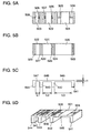
- Figs. 5A through 5D show the structure of an acceleration sensor element, which is the major component of acceleration sensors 101 through 103.
- Figs. 5A through 5D shows an acceleration sensor element having a both-ends-supported beam structure.
- Fig. 5A is a top view;
- Fig. 5B is a bottom view;
- Fig. 5C is a side view;
- Fig. 5D is a perspective view.
- Each of free vibrating sections 545 through 547 shown in Figs. 5A through 5D has a bimorph structure in which distortion and vibration occurs when an impactive force is applied.
- Free vibrating sections 545, 546, and 547 have main electrodes 501, 502, and 503 on each upper surface thereof; and have main electrodes 520, 521, and 522 on each lower surface thereof, respectively.
- Draw-out electrodes 504 and 505 are connected with main electrode 501; draw-out electrodes 506 and 507 are connected with main electrode 502; and draw-out electrodes 508 and 509 are connected with main electrode 503 to establish electrical connections, respectively.
- Free vibrating sections 545 through 547 generate electric charges according to distortion in shape due to their bimorph structures.
- the electric charge generated on each upper surface of free vibrating sections 545, 546, and 547 is carried to main electrodes 501, 502, and 503, respectively, and further carried to draw-out electrodes 504 and 505; 506 and 507; 508 and 509, respectively.
- the electric charge generated on each lower surface of free vibrating sections 545, 546, and 547 is carried to main electrodes 520, 521, and 522, respectively, and further carried to draw-out electrodes 523 and 524; 525 and 526; 527 and 528, respectively.
- the electric charges carried to main electrodes 520 through 522 are opposite in polarity to those carried to main electrodes 501 through 503.
- Draw-out electrodes 523 through 528 are extended to the bottom of supporters 541 through 544, via the side surfaces of the supporters, and are exposed at the bottom of the each supporter.
- draw-out electrodes 504 through 509 and 523 through 528 are formed as a part of free vibrating sections 545 through 547 is as follows: such a structure can avoid cancellation of the drawn out electric charge due to stress distribution in free vibrating sections 545 through 547.
- each width of draw-out electrodes 504 and 505 is determined less than one-fifth of that of main electrode 501.
- Free vibrating sections 545, 546, and 547 have lengths of L3, L2, and L1, respectively, and in which L3 is the longest, and L1 is the shortest. Free vibrating sections 545 through 547 are electrically separated each other.
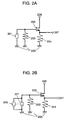
- Fig. 2A shows the circuit diagram of acceleration sensors 101 through 103 shown in Fig. 1.
- Acceleration sensor element 201 is the one the same as shown in Figs. 5A through 5D.
- One of draw-out electrodes 523 and 524 shown in Figs. 5A through 5D is connected to ground 205 of Fig. 2A.
- one of draw-out electrodes 504 and 505 shown in Figs. 5A through 5D is connected to resistor 202 of Fig. 2A.
- the electric charge obtained from draw-out electrode 504 or 505 is converted through resistor 202 into current. Besides, feeding the current through resistor 202 allows resistor 202 to generate voltage.
- FET field-effect transistor
- the source of FET 203 is connected, through terminal 206, to the positive side of a power-supplying unit; the gate is connected to the acceleration sensor element 201 and resistor 202; and the drain is connected to resistor 204.
- the other terminal of resistor 204 is connected to ground 205.
- the potential of the drain is taken out through terminal 207. Forming the circuit like this allows terminal 207 to have lower output impedance.
- the acceleration sensor element shown in Figs. 5A through 5D also has free vibrating sections 546 and 547. Each signal obtained from the two sections is similarly processed, as shown in Fig. 2A.
- a signal from terminal 207 is fed to the corresponding one of switches 106 through 108.
- Acceleration sensor element 201 generally bears capacitance - working the capacitance with resistor 202 inevitably forms a filter that cuts off low band frequencies. Therefore, the signals generated in acceleration sensor element 201 are decreased in low frequency band.
- Fig. 3 is a flow chart illustrating the routine of measuring drop impact in the circuit shown in Fig. 1.
- an acceleration sensor including the free vibrating section with the highest sensibility and the lowest resonance frequency is selected from free vibrating sections 545 through 547 of different lengths shown in Figs. 5A through 5D; acceleration sensor 101 including free vibrating section 545 can provide the highest sensibility and the lowest resonance frequency, that is, "S" takes on 1.
- step 301 among switches 106 through 108, only one switch associated with the acceleration sensor selected in step 300 is closed, whereby sensor switching is performed. At the moment, since "S" retains the value of 1, only switch 106 of Fig. 1 is closed.
- step 302 the drop down test begins.
- step 303 drop impact caused by the drop-down is measured.
- Amplifying circuit 104 amplifies signals from acceleration sensor 101 generated by the drop impact and then outputs the measured result (i.e., impact acceleration) through terminal 110 shown in Fig. 1
- step 304 logic circuit 105 evaluates whether the output signal from amplifying circuit 104 stays within a threshold or not, and whether resonance occurs or not.
- step 306 if the impact acceleration stays within the threshold, the acceleration is displayed in step 312. A display for showing the impact acceleration is not shown in Fig. 1.
- step 307 the value currently stored in S is compared with the value stored in N.
- step 311 If the comparison finds that the value of S equals to that of N - which means that each of the output signals generated from free vibrating sections 545 through 547 shown in Figs. 5A through 5D via amplifying circuit 104 exceeds the threshold, the procedure goes to step 311, where an error indication is shown on the display.
- step 310 the procedure goes to step 310 where the value of S (that indicates a sensor number) is updated. That is, S is incremented by 1 in step 310, and then the procedure goes back to step 301. According to the updated S, next acceleration sensor is selected in step 301, and the drop impact measurement is resumed from step 302.
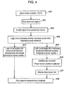
- Fig. 4 is another flow chart illustrating the routine of measuring drop impact in the circuit shown in Fig. 1.
- the flow chart shown in Fig. 3 if the result of the drop impact measurement obtained at step 303 exceeds the threshold of S representing a sensor number, the value of S is incremented by 1 in step 310, and then the drop-impact measurement is resumed at step 302.
- the logic circuit evaluates output signals to find a proper sensor number, and then the drop impact measurement is resumed with the acceleration sensor corresponding to the sensor number.
- step 400 S initially takes on 1, and the drop impact test begins at step 401.
- step 402 amplifying circuit 104 amplifies the output signal of acceleration sensor 101 that has been entered through switch 106.
- logic circuit 105 evaluates whether the output signal from amplifying circuit 104 stays within a threshold or not, and whether resonance occurs or not.
- step 404 if the logic circuit evaluates that the impact acceleration stays within a threshold, the acceleration is displayed in step 408. A display for showing the impact acceleration is not shown in Fig. 1.
- logic circuit 105 selects a proper sensor number according to the output signal of amplifying circuit 104 in step 406.
- step 407 a switch corresponding to the sensor number selected above is closed to resume the drop impact test.
- step 408 the drop impact is measured and displayed.
- An acceleration sensor for detecting drop impact is required to have differently ranged resonance frequencies, that is, desirably to have various frequencies, not only one.
- the resonance frequency "fr" varies inversely with the square of the length of the free vibrating section.
- the acceleration sensor element shown in Figs. 5A through 5D has free vibrating sections 545 through 547 of different lengths, thereby offering various resonance frequencies.
- the acceleration sensor element shown in Figs. 5A through 5D is thus ready for various resonance frequencies.
- FIG. 7A through 7C shows an acceleration sensor element having a cantilever beam structure.
- Fig. 7A is a top view
- Fig. 7B is a side view
- Fig. 7C is a perspective view.
- the structure in which supporter 744 holds each one end of free vibrating sections 741 through 743 forms into a cantilever beam.
- Free vibrating sections 741, 742, and 743 have main electrodes 701, 702, and 703 on the upper surfaces thereof, and main electrodes 721, 722, and 723 on the lower surfaces thereof, respectively.
- Draw-out electrodes 724, 725, and 726 which are formed on the bottom of supporter 744, are electrically connected with main electrodes 721, 722, and 723, respectively.
- FIG. 8A is a top view
- Fig. 8B is a bottom view
- Fig. 8C is a perspective view.
- the structure in which supporter 843 holds each one end of free vibrating sections 841 and 842 forms into a cantilever beam.
- Free vibrating section 841 has main electrode 801 on the upper surface thereof, and main electrode 821 on the lower surface thereof.
- free vibrating section 842 has main electrode 802 on the upper surface thereof, and main electrode 822 on the lower surface thereof.
- Draw-out electrodes 803 and 804 are electrically connected with main electrodes 801 and 802, respectively.
- Draw-out electrode 823 which is formed on the bottom of supporter 843, runs across side 844 of the supporter and reaches main electrode 821 to have electric connections.
- draw-out electrode 824 which is also formed on the bottom of supporter 843, runs across the side opposite to side 844 of the supporter and reaches main electrode 822 to have electric connections.
- the cantilever beam structure When comparisons are made between the acceleration sensor element formed into a cantilever beam structure shown in Figs. 7A through 7C and Figs. 8A through 8C; and the acceleration sensor element formed into a both ends-supported beam structure shown in Figs. 5A through 5D, the cantilever beam structure generates four to five times more amount of output electrical charge than the both ends-supported beam structure does, provided they have same dimensions. Therefore, amplifying circuit 104 of Fig. 1, which is necessary for the acceleration sensor element having the both ends-supported beam shown in Figs. 5A through 5D, can be eliminated by using the cantilever beam structure. Eliminating the amplifying circuit can provide a low-cost drop impact measuring system. Besides, the parallel arrangement of free vibrating sections 741 through 743 allows the whole structure of the acceleration sensor element to be compact, accordingly providing a downsized drop impact measuring system.
- the structure of the embodiment can provide the drop impact measuring system that easily measures an impact acceleration of even more than 1000G having great variations in resonance frequency.
- the structure of the embodiment also provides an acceleration sensor element capable of detecting impact acceleration of various resonance frequencies.
- Fig. 1 also shows a circuit diagram of the drop impact measuring system of the second embodiment.
- Fig. 2B shows a circuit diagram of the acceleration sensor of the second embodiment.
- Figs. 3 and 4 are flow charts illustrating the routine of detecting drop impact acceleration in the drop impact measuring system of the second embodiment.
- Each of Figs. 6A through 6C shows an acceleration sensor element having a structure of cantilever beam of the second embodiment.
- Fig. 6A is a top view
- Fig. 6B is a bottom view
- Fig. 6C is a perspective view.
- Each one end of free vibrating sections 641 through 644 are supportably fixed by supporter 645.
- Free vibrating sections 641, 642, 643, and 644 have main electrodes 601, 602, 603, and 604 on the upper surfaces thereof; and have main electrodes 620, 621, 622, and 623 on the lower surfaces thereof, respectively.
- Main electrodes 601, 602, 603, and 604 are electrically connected with draw-out electrodes 605, 606, 607, and 608, respectively.
- main electrodes 620, 621, 622, and 623 are electrically connected with draw-out electrodes 624, 625, 626, and 627, respectively.
- Draw-out electrodes 624 through 627 are exposed from the bottom of supporter 645.
- Free vibrating sections 641, 642, 643, and 644 are of the same length, which are represented by L4, L5, L6, and L7
- acceleration sensor element 220 is formed of free vibrating section 641; main electrodes 601 and 620; and draw-out electrodes 605 and 624.
- main electrodes 601 and 620 are used for sensor element 220; any one of the rest three is to be employed for sensor element 221.
- Draw-out electrodes 624 through 627 are connected to ground 225.
- Such structured acceleration sensor serves as acceleration sensor 101 shown in Fig. 1.
- acceleration sensors 102 and 103 are formed in the same manner with sensor 101, each acceleration sensor element used for these three sensors has differently ranged resonance frequency. That is, the acceleration sensor can offer various resonance frequencies.
- the acceleration sensor element introduced in the second embodiment by virtue of the structure in which the free vibrating sections of same resonance frequencies are electrically connected in parallel, has no decrease in electric capacity if the sensor element itself is miniaturized. Therefore, the structure described in the second embodiment can provide a high-noise-durability acceleration sensor element and a drop impact measuring system using the sensor element.
- a prior-art acceleration sensor element as described above, lowers electric capacity as it is downsized.
- the "Fc" given by the Expression 1, which represents low-band cut-off frequency takes on a large value.
- the acceleration sensor element of the second embodiment has no decrease in electric capacity, thereby keeping the low-band cut-off frequency "Fc" from getting high.
- the drop impact measuring system and the acceleration sensor element employed for the system of the present invention can cope well with wide ranged resonance frequencies and great impact acceleration. Besides, the acceleration sensor element can be miniaturized and improved in durability of noise characteristics.
Landscapes
- Physics & Mathematics (AREA)
- General Physics & Mathematics (AREA)
- Pressure Sensors (AREA)
- Measurement Of Length, Angles, Or The Like Using Electric Or Magnetic Means (AREA)
- Measurement Of Mechanical Vibrations Or Ultrasonic Waves (AREA)
Abstract
The drop impact measuring system has i) a plurality of bimorph-type
acceleration sensor containing a plurality of free vibrating sections each of
which has individual draw-out electrodes; ii) a switch section for selecting
output from the bimorph-type acceleration sensors; iii) an amplifying circuit for
amplifying a signal applied via the switch section from the acceleration sensors;
and iv) a logic circuit for logically evaluating the output from the amplifying
circuit and controlling the switch section according to the result acquired from
the logical evaluation.
Description
The present invention relates to a drop impact measuring system used for
a drop impact test on mobile electronic equipment including a mobile phone, and
also relates to an acceleration sensor element employed for the drop impact
measuring system.
For mobile electronic equipment including a mobile phone, a notebook
size computer, a mobile cassette player, compact disc (CD) player, and mini disc
(MD) player, drop-down is an ever-present accident when considering its
intended use. Accordingly, protecting the equipment from impact caused by the
drop-down has now been a growing need. A typical failure comes from
distortion of a motherboard mounted on the equipment due to drop-down impact,
by which some on-board components have shorts in the wiring, or come off the
board. Therefore, to protect the equipment from such accidents, following steps
should be taken: i) selecting a material and a structure of electronic equipment
to be tested; ii) determining a drop-down height and direction; iii) simulating
drop-down impact acceleration applied to each section of the equipment; and
then iv) getting feedback from the result and improving the design of the inner
structure, for example, the position and method of installing a circuit board.
However, the drop-down impact acceleration during falling greatly varies
between falling objects, and the acceleration applied to an object has significant
magnitude. Furthermore, resonance frequency caused by drop impact greatly
depends on the structure of an object. The reasons above have been obstacles
to detection of drop-down impact acceleration applied to a falling object.
The drop impact measuring system has i) a plurality of bimorph-type
acceleration sensors containing a plurality of free vibrating sections each of
which has individual draw-out electrodes; ii) a switch section for selecting
output of the bimorph acceleration sensors obtained through the draw-out
electrodes; iii) an amplifying circuit for amplifying at least one of voltage and
current applied via the switch section from the bimorph acceleration sensors;
and iv) a logic circuit for logically evaluating the output from the amplifying
circuit and controlling the switch section according to the result acquired from
the logical evaluation.
A bimorph acceleration sensor element is formed of the free vibrating
sections having cantilever beams. Signals generated at the free vibrating
section are fed through the draw-out electrodes to the switch section.
The bimorph acceleration sensor element is also formed of the free
vibrating section having both-ends-supported beams. Signals generated at the
free vibrating section are fed through the draw-out electrodes to the switch
section.
Fig. 1 shows a circuit diagram of a drop impact measuring system in
accordance with a first embodiment of the present invention. Acceleration
sensors 101, 102, and 103 are connected to switches 106, 107, and 108,
respectively. Sensors 101 through 103 are also connected to ground 109. By
closing one of switches 106 through 108, an output signal from one of
acceleration sensors 101 through 103 is fed into amplifying circuit 104 to be
amplified. Amplifying circuit 104 outputs a signal, which corresponds to
acceleration, via terminal 110. Logic circuit 105 evaluates whether or not the
signal from amplifying circuit 104 stays within a predetermined threshold, and
whether resonance occurs or not, accordingly outputs logically evaluated result.
Logic circuit 105 determines which one of switches 106 through 108 should be
closed, according to the logical evaluation, thereby controlling switches 106
through 108.
Figs. 5A through 5D show the structure of an acceleration sensor element,
which is the major component of acceleration sensors 101 through 103. Figs.
5A through 5D shows an acceleration sensor element having a both-ends-supported
beam structure. Fig. 5A is a top view; Fig. 5B is a bottom view; Fig.
5C is a side view; and Fig. 5D is a perspective view. Each of free vibrating
sections 545 through 547 shown in Figs. 5A through 5D has a bimorph structure
in which distortion and vibration occurs when an impactive force is applied.
Free vibrating sections 545, 546, and 547 have main electrodes 501, 502, and
503 on each upper surface thereof; and have main electrodes 520, 521, and 522
on each lower surface thereof, respectively. Draw-out electrodes 504 and 505
are connected with main electrode 501; draw-out electrodes 506 and 507 are
connected with main electrode 502; and draw-out electrodes 508 and 509 are
connected with main electrode 503 to establish electrical connections,
respectively. Free vibrating sections 545 through 547 generate electric charges
according to distortion in shape due to their bimorph structures. The electric
charge generated on each upper surface of free vibrating sections 545, 546, and
547 is carried to main electrodes 501, 502, and 503, respectively, and further
carried to draw-out electrodes 504 and 505; 506 and 507; 508 and 509,
respectively. On the other hand, The electric charge generated on each lower
surface of free vibrating sections 545, 546, and 547 is carried to main electrodes
520, 521, and 522, respectively, and further carried to draw-out electrodes 523
and 524; 525 and 526; 527 and 528, respectively. The electric charges carried to
main electrodes 520 through 522 are opposite in polarity to those carried to
main electrodes 501 through 503. Draw-out electrodes 523 through 528 are
extended to the bottom of supporters 541 through 544, via the side surfaces of
the supporters, and are exposed at the bottom of the each supporter.
The deformation of free vibrating sections 545 through 547 creates
oppositely polarized electric charges: one is drawn out by draw-out electrodes
504 through 509 disposed on the upper surface of free vibrating sections 545
through 547; the other is drawn out by draw-out electrodes 523 through 528
exposed at the bottom of supporters 541 through 544.
The reason why draw-out electrodes 504 through 509 and 523 through
528 are formed as a part of free vibrating sections 545 through 547 is as follows:
such a structure can avoid cancellation of the drawn out electric charge due to
stress distribution in free vibrating sections 545 through 547. in the structure
above, for example, each width of draw-out electrodes 504 and 505 is determined
less than one-fifth of that of main electrode 501.
Free vibrating sections 545, 546, and 547 have lengths of L3, L2, and L1,
respectively, and in which L3 is the longest, and L1 is the shortest. Free
vibrating sections 545 through 547 are electrically separated each other.
Fig. 2A shows the circuit diagram of acceleration sensors 101 through 103
shown in Fig. 1. Acceleration sensor element 201 is the one the same as shown
in Figs. 5A through 5D. One of draw-out electrodes 523 and 524 shown in Figs.
5A through 5D is connected to ground 205 of Fig. 2A. On the other hand, one of
draw-out electrodes 504 and 505 shown in Figs. 5A through 5D is connected to
resistor 202 of Fig. 2A. The electric charge obtained from draw-out electrode
504 or 505 is converted through resistor 202 into current. Besides, feeding the
current through resistor 202 allows resistor 202 to generate voltage. In the
case that resistor 202 is required to have large resistance value more than 1 MΩ,
employing field-effect transistor (FET) 203 allows the circuit to have lower
impedance. The source of FET 203 is connected, through terminal 206, to the
positive side of a power-supplying unit; the gate is connected to the acceleration
sensor element 201 and resistor 202; and the drain is connected to resistor 204.
The other terminal of resistor 204 is connected to ground 205. The potential of
the drain is taken out through terminal 207. Forming the circuit like this
allows terminal 207 to have lower output impedance.
The acceleration sensor element shown in Figs. 5A through 5D also has
free vibrating sections 546 and 547. Each signal obtained from the two sections
is similarly processed, as shown in Fig. 2A.
A signal from terminal 207 is fed to the corresponding one of switches 106
through 108.
In the embodiment, ID numbers 1 through 3 are assigned to the
acceleration sensors having free vibrating sections 545 through 547, respectively,
and a letter "S" indicates the ID number: S = 1 in acceleration sensor 101
containing free vibrating section 545; S = 2 in acceleration sensor 102 containing
free vibrating section 546; and S = 3 in acceleration sensor 103 containing free
vibrating section 547. Similarly, a letter "N" represents the total number of
acceleration sensors: N = 3 in the acceleration sensors shown in Figs. 5A
through 5D.
Although the explanation above introduces the structure in which i)
generating current by moving the electric charge obtained from one of draw-out
electrodes 504 and 505; ii) converting the current into voltage by feeding
through resistor 202; and then iii) amplifying the voltage, it is not limited
thereto: the structure in which current is directly amplified is also acceptable.
Fig. 3 is a flow chart illustrating the routine of measuring drop impact in
the circuit shown in Fig. 1. In the first step 300, an acceleration sensor
including the free vibrating section with the highest sensibility and the lowest
resonance frequency is selected from free vibrating sections 545 through 547 of
different lengths shown in Figs. 5A through 5D; acceleration sensor 101
including free vibrating section 545 can provide the highest sensibility and the
lowest resonance frequency, that is, "S" takes on 1.
In step 301, among switches 106 through 108, only one switch associated
with the acceleration sensor selected in step 300 is closed, whereby sensor
switching is performed. At the moment, since "S" retains the value of 1, only
switch 106 of Fig. 1 is closed.
In step 302, the drop down test begins.
In step 303, drop impact caused by the drop-down is measured.
Amplifying circuit 104 amplifies signals from acceleration sensor 101 generated
by the drop impact and then outputs the measured result (i.e., impact
acceleration) through terminal 110 shown in Fig. 1
In step 304, logic circuit 105 evaluates whether the output signal from
amplifying circuit 104 stays within a threshold or not, and whether resonance
occurs or not.
In step 306, if the impact acceleration stays within the threshold, the
acceleration is displayed in step 312. A display for showing the impact
acceleration is not shown in Fig. 1.
On the other hand, if the impact acceleration exceeds the threshold, the
procedure goes to step 307. In step 307, the value currently stored in S is
compared with the value stored in N.
If the comparison finds that the value of S equals to that of N - which
means that each of the output signals generated from free vibrating sections 545
through 547 shown in Figs. 5A through 5D via amplifying circuit 104 exceeds
the threshold, the procedure goes to step 311, where an error indication is shown
on the display.
On the other hand, if S does not reach N, the procedure goes to step 310
where the value of S (that indicates a sensor number) is updated. That is, S is
incremented by 1 in step 310, and then the procedure goes back to step 301.
According to the updated S, next acceleration sensor is selected in step 301, and
the drop impact measurement is resumed from step 302.
Fig. 4 is another flow chart illustrating the routine of measuring drop
impact in the circuit shown in Fig. 1. According to the flow chart shown in Fig.
3, if the result of the drop impact measurement obtained at step 303 exceeds the
threshold of S representing a sensor number, the value of S is incremented by 1
in step 310, and then the drop-impact measurement is resumed at step 302.
On the other hand, in the flow chart of Fig. 4, even if the first result of the
measurement exceeds the threshold of S, the logic circuit evaluates output
signals to find a proper sensor number, and then the drop impact measurement
is resumed with the acceleration sensor corresponding to the sensor number.
In step 400, S initially takes on 1, and the drop impact test begins at step
401. Next, in step 402, amplifying circuit 104 amplifies the output signal of
acceleration sensor 101 that has been entered through switch 106.
In step 403, logic circuit 105 evaluates whether the output signal from
amplifying circuit 104 stays within a threshold or not, and whether resonance
occurs or not.
In step 404, if the logic circuit evaluates that the impact acceleration stays
within a threshold, the acceleration is displayed in step 408. A display for
showing the impact acceleration is not shown in Fig. 1.
On the other hand, if the impact acceleration exceeds the threshold, logic
circuit 105 selects a proper sensor number according to the output signal of
amplifying circuit 104 in step 406.
In step 407, a switch corresponding to the sensor number selected above
is closed to resume the drop impact test.
In step 408, the drop impact is measured and displayed.
An acceleration sensor for detecting drop impact is required to have
differently ranged resonance frequencies, that is, desirably to have various
frequencies, not only one.
In the acceleration sensor element shown in Figs. 5A through 5D, suppose
that "fr" represents the resonance frequency; "L" represents the length of the
free vibrating section; "t" represents the thickness; and "α" represents a
constant, "fr" is given by the expression below:
Fr ∝ α × T/L2
That is, the resonance frequency "fr" varies inversely with the square of
the length of the free vibrating section. The acceleration sensor element shown
in Figs. 5A through 5D has free vibrating sections 545 through 547 of different
lengths, thereby offering various resonance frequencies. The acceleration
sensor element shown in Figs. 5A through 5D is thus ready for various
resonance frequencies.
Employing such structured acceleration sensor element for a drop impact
measuring system can easily detect impact acceleration, even in the case that a
resonance frequency at the drop down of an object is unpredictable in advance.
Accordingly, it will contribute to easy structural design of the housing.
Each of Figs. 7A through 7C, and Figs. 8A through 8D shows an
acceleration sensor element having a cantilever beam structure.
Fig. 7A is a top view, Fig. 7B is a side view, and Fig. 7C is a perspective
view. The structure in which supporter 744 holds each one end of free vibrating
sections 741 through 743 forms into a cantilever beam. Free vibrating sections
741, 742, and 743 have main electrodes 701, 702, and 703 on the upper surfaces
thereof, and main electrodes 721, 722, and 723 on the lower surfaces thereof,
respectively. Draw-out electrodes 724, 725, and 726, which are formed on the
bottom of supporter 744, are electrically connected with main electrodes 721,
722, and 723, respectively.
Each of Figs. 8A through 8D shows another acceleration sensor element
having the cantilever beam structure. Fig. 8A is a top view, Fig. 8B is a bottom
view, and Fig. 8C is a perspective view. The structure in which supporter 843
holds each one end of free vibrating sections 841 and 842 forms into a cantilever
beam. Free vibrating section 841 has main electrode 801 on the upper surface
thereof, and main electrode 821 on the lower surface thereof. Similarly, free
vibrating section 842 has main electrode 802 on the upper surface thereof, and
main electrode 822 on the lower surface thereof. Draw-out electrodes 803 and
804 are electrically connected with main electrodes 801 and 802, respectively.
Draw-out electrode 823, which is formed on the bottom of supporter 843, runs
across side 844 of the supporter and reaches main electrode 821 to have electric
connections. Similarly, draw-out electrode 824, which is also formed on the
bottom of supporter 843, runs across the side opposite to side 844 of the
supporter and reaches main electrode 822 to have electric connections.
When comparisons are made between the acceleration sensor element
formed into a cantilever beam structure shown in Figs. 7A through 7C and Figs.
8A through 8C; and the acceleration sensor element formed into a both ends-supported
beam structure shown in Figs. 5A through 5D, the cantilever beam
structure generates four to five times more amount of output electrical charge
than the both ends-supported beam structure does, provided they have same
dimensions. Therefore, amplifying circuit 104 of Fig. 1, which is necessary for
the acceleration sensor element having the both ends-supported beam shown in
Figs. 5A through 5D, can be eliminated by using the cantilever beam structure.
Eliminating the amplifying circuit can provide a low-cost drop impact
measuring system. Besides, the parallel arrangement of free vibrating sections
741 through 743 allows the whole structure of the acceleration sensor element to
be compact, accordingly providing a downsized drop impact measuring system.
Employing the structure explained in the first embodiment can provide
the drop impact measuring system that easily measures an impact acceleration
of even more than 1000G having great variations in resonance frequency. At
the same time, the structure of the embodiment also provides an acceleration
sensor element capable of detecting impact acceleration of various resonance
frequencies.
Fig. 1 also shows a circuit diagram of the drop impact measuring system
of the second embodiment. Fig. 2B shows a circuit diagram of the acceleration
sensor of the second embodiment. Figs. 3 and 4 are flow charts illustrating the
routine of detecting drop impact acceleration in the drop impact measuring
system of the second embodiment. Each of Figs. 6A through 6C shows an
acceleration sensor element having a structure of cantilever beam of the second
embodiment.
Fig. 6A is a top view, Fig. 6B is a bottom view, and Fig. 6C is a perspective
view. Each one end of free vibrating sections 641 through 644 are supportably
fixed by supporter 645. Free vibrating sections 641, 642, 643, and 644 have
main electrodes 601, 602, 603, and 604 on the upper surfaces thereof; and have
main electrodes 620, 621, 622, and 623 on the lower surfaces thereof,
respectively. Main electrodes 601, 602, 603, and 604 are electrically connected
with draw-out electrodes 605, 606, 607, and 608, respectively. Similarly, main
electrodes 620, 621, 622, and 623 are electrically connected with draw-out
electrodes 624, 625, 626, and 627, respectively. Draw-out electrodes 624
through 627 are exposed from the bottom of supporter 645. Free vibrating
sections 641, 642, 643, and 644 are of the same length, which are represented by
L4, L5, L6, and L7, respectively.
Using the acceleration sensor element shown in Figs. 6A through 6C, the
acceleration sensor is formed, as shown in Fig. 2B. That is, acceleration sensor
element 220 is formed of free vibrating section 641; main electrodes 601 and
620; and draw-out electrodes 605 and 624. Of four acceleration sensor
elements shown in Figs. 6A through 6C, one is used for sensor element 220; any
one of the rest three is to be employed for sensor element 221. Draw-out
electrodes 624 through 627 are connected to ground 225. On the other hand,
draw-out electrodes 605 through 608, which are electrically connected in
parallel, and then connected to resistor 222. Resistors 222 and 224, FET223,
terminals 226 and 227 shown in Fig. 2B act the same as resistors 202 and 204,
FET203, terminals 206 and 207 shown in Fig. 2A, respectively, therefore the
explanation of the components above will be omitted. Such structured
acceleration sensor serves as acceleration sensor 101 shown in Fig. 1.
Although acceleration sensors 102 and 103 are formed in the same
manner with sensor 101, each acceleration sensor element used for these three
sensors has differently ranged resonance frequency. That is, the acceleration
sensor can offer various resonance frequencies.
To measure greater drop impact acceleration, miniaturizing the
acceleration sensor element and increasing mechanical strength seems to be an
effective way. According to a prior-art acceleration sensor element, however,
miniaturization of a sensor element has lowered electric capacity and thereby
degraded durability of noise characteristics of the sensor element itself.
Whereas the sensor element introduced in the second embodiment, by virtue of
the structure in which the free vibrating sections of same resonance frequencies
are electrically connected in parallel, has no decrease in electric capacity if the
sensor element itself is miniaturized. Therefore, the structure described in the
second embodiment can provide a high-noise-durability acceleration sensor
element and a drop impact measuring system using the sensor element.
A prior-art acceleration sensor element, as described above, lowers
electric capacity as it is downsized. As a result, the "Fc" given by the
Expression 1, which represents low-band cut-off frequency, takes on a large
value. Whereas the acceleration sensor element of the second embodiment has
no decrease in electric capacity, thereby keeping the low-band cut-off frequency
"Fc" from getting high.
Although the acceleration sensor of the second embodiment is formed of
the acceleration sensor element having the shape illustrated in Figs. 6A through
6C, it is not limited thereto: the similar effect can be obtained by the structure
having free vibrating sections 741, 742, and 743 (Figs. 7A through 7C) of same
lengths, i.e., L10 = L9 = L8; the structure having free vibrating sections 841 and
842 (Figs. 8A through 8C) of same lengths, i.e., L11 = L12; or the structure
having free vibrating sections 545, 546, and 547 (Figs. 5A through 5D) of same
lengths, i.e., L3 = L2 = L1.
The drop impact measuring system and the acceleration sensor element
employed for the system of the present invention can cope well with wide ranged
resonance frequencies and great impact acceleration. Besides, the acceleration
sensor element can be miniaturized and improved in durability of noise
characteristics.
Claims (7)
- A drop impact measuring system comprising:a) a plurality of bimorph-type acceleration sensors containing a plurality of free vibrating sections each of which has individual draw-out electrodes;b) a switch section for selecting output of the plurality of bimorph acceleration sensors obtained through the draw-out electrodes;c) an amplifying circuit for amplifying at least one of voltage and current applied via the switch section from the bimorph acceleration sensors; andd) a logic circuit for logically evaluating the output from the amplifying circuit and controlling the switch section according to result acquired from the logical evaluation.
- A bimorph-type acceleration sensor element, which is used for a bimorph-type acceleration sensor, comprising i) a plurality of free vibrating sections having a cantilever beam structure; and ii) draw-out electrodes for drawing out a signal generated in the free vibrating sections.
- The bimorph-type acceleration sensor element of claim 2, wherein the plurality of the free vibrating sections are of different lengths and are electrically independent.
- The bimorph-type acceleration sensor element of claim 2, wherein the plurality of the free vibrating sections are of identical length and are electrically connected in parallel.
- A bimorph-type acceleration sensor element, which is used for a bimorph-type acceleration sensor, comprising i) a plurality of free vibrating sections having a both-ends-supported beam structure; and ii) draw-out electrodes for drawing out a signal generated in the free vibrating sections.
- The bimorph-type acceleration sensor element of claim 5, wherein the plurality of the free vibrating sections are of different lengths and are electrically independent.
- The bimorph-type acceleration sensor element of claim 5, wherein the plurality of the free vibrating sections are of identical length and are electrically connected in parallel.
Applications Claiming Priority (3)
| Application Number | Priority Date | Filing Date | Title |
|---|---|---|---|
| JP2001242871 | 2001-08-09 | ||
| JP2001242871 | 2001-08-09 | ||
| PCT/JP2002/008053 WO2003016920A1 (en) | 2001-08-09 | 2002-08-07 | Drop shock measurement system and acceleration sensor element used in the same |
Publications (2)
| Publication Number | Publication Date |
|---|---|
| EP1416284A1 true EP1416284A1 (en) | 2004-05-06 |
| EP1416284A4 EP1416284A4 (en) | 2009-06-10 |
Family
ID=19073076
Family Applications (1)
| Application Number | Title | Priority Date | Filing Date |
|---|---|---|---|
| EP02758794A Withdrawn EP1416284A4 (en) | 2001-08-09 | 2002-08-07 | FALL SHOCK MEASURING SYSTEM AND ACCELERATION DETECTOR ELEMENT USED THEREIN |
Country Status (6)
| Country | Link |
|---|---|
| US (3) | US20040025564A1 (en) |
| EP (1) | EP1416284A4 (en) |
| JP (1) | JPWO2003016920A1 (en) |
| CN (1) | CN1258092C (en) |
| TW (1) | TW546477B (en) |
| WO (1) | WO2003016920A1 (en) |
Cited By (1)
| Publication number | Priority date | Publication date | Assignee | Title |
|---|---|---|---|---|
| US11826901B2 (en) | 2018-11-28 | 2023-11-28 | Samsung Electronics Co., Ltd. | Electronic device, and method for sensing state thereof |
Families Citing this family (8)
| Publication number | Priority date | Publication date | Assignee | Title |
|---|---|---|---|---|
| US7239064B1 (en) | 2004-10-15 | 2007-07-03 | Morgan Research Corporation | Resettable latching MEMS temperature sensor apparatus and method |
| US8387452B2 (en) * | 2007-07-18 | 2013-03-05 | Pirelli Tyre S.P.A. | Method and system for generating electrical energy within a vehicle tyre |
| US8011237B2 (en) * | 2008-02-22 | 2011-09-06 | Hong Kong Applied Science And Technology Research Institute Co., Ltd. | Piezoelectric module for energy harvesting, such as in a tire pressure monitoring system |
| CN102859369B (en) * | 2010-02-02 | 2016-01-20 | Skf公司 | Arrangement of pressure sensors in an accelerometer |
| JP2011185828A (en) * | 2010-03-10 | 2011-09-22 | Fuji Electric Co Ltd | Acceleration sensor |
| DE102017102614A1 (en) * | 2017-02-09 | 2018-08-09 | Efaflex Tor- Und Sicherheitssysteme Gmbh & Co. Kg | Door panel crash detection system, door panel crash detection system, and door panel crash detection method |
| US20220005341A1 (en) * | 2018-11-07 | 2022-01-06 | World Wide Warranty Life Services Inc. | Method and system for detecting presence of a protective case on a portable electronic device during drop impact |
| CN114631071A (en) | 2019-10-18 | 2022-06-14 | 全球人寿担保服务有限公司 | Method and system for detecting existence of protective shell on electronic equipment |
Family Cites Families (26)
| Publication number | Priority date | Publication date | Assignee | Title |
|---|---|---|---|---|
| JPS5436771A (en) * | 1977-08-26 | 1979-03-17 | Shimadzu Corp | Vibration detector |
| JPS55162037A (en) * | 1979-06-04 | 1980-12-17 | Nippon Soken Inc | Knocking detector for internal combustion engine |
| US4431935A (en) * | 1981-09-15 | 1984-02-14 | Rockwell International Corporation | Sensor structure incorporating multiple piezoelectric generators |
| CA1225694A (en) * | 1983-12-09 | 1987-08-18 | Nippon Telegraph And Telephone Corporation | Piezoelectric actuator using bimorph element |
| US4736629A (en) * | 1985-12-20 | 1988-04-12 | Silicon Designs, Inc. | Micro-miniature accelerometer |
| JPH076850B2 (en) * | 1987-06-04 | 1995-01-30 | 横河電機株式会社 | Temperature measurement circuit |
| EP0325674A1 (en) * | 1988-01-29 | 1989-08-02 | Kistler Instrumente AG | Transducer element for measuring of rotational acceleration |
| US4855544A (en) * | 1988-09-01 | 1989-08-08 | Honeywell Inc. | Multiple level miniature electromechanical accelerometer switch |
| US4901586A (en) * | 1989-02-27 | 1990-02-20 | Sundstrand Data Control, Inc. | Electrostatically driven dual vibrating beam force transducer |
| EP0567938B1 (en) * | 1992-04-30 | 1998-03-18 | Texas Instruments Incorporated | Digital accelerometer |
| JP3148945B2 (en) | 1992-05-28 | 2001-03-26 | 株式会社トーキン | Acceleration sensor |
| US6043588A (en) * | 1995-07-18 | 2000-03-28 | Murata Manufacturing Co., Ltd. | Piezoelectric sensor and acceleration sensor |
| US6098460A (en) * | 1995-10-09 | 2000-08-08 | Matsushita Electric Industrial Co., Ltd. | Acceleration sensor and shock detecting device using the same |
| DE19625618C1 (en) * | 1996-06-26 | 1997-09-04 | Siemens Ag | Impact detector for automobile |
| US6058778A (en) * | 1997-10-24 | 2000-05-09 | Stmicroelectronics, Inc. | Integrated sensor having plurality of released beams for sensing acceleration |
| JP2000002714A (en) * | 1998-04-13 | 2000-01-07 | Matsushita Electric Ind Co Ltd | Piezoelectric acceleration sensor, acceleration detection method, and method of manufacturing piezoelectric acceleration sensor |
| CN1138149C (en) * | 1998-05-19 | 2004-02-11 | 松下电器产业株式会社 | Acceleration sensor and acceleration device using the acceleration sensor |
| KR100563982B1 (en) * | 1998-10-19 | 2006-03-29 | 가부시키가이샤 야스카와덴키 | Clean robot safety protection device |
| JP3339425B2 (en) * | 1998-10-19 | 2002-10-28 | 株式会社村田製作所 | Acceleration sensor and acceleration detection device |
| JP2000155126A (en) * | 1998-11-19 | 2000-06-06 | Toyota Central Res & Dev Lab Inc | Acceleration sensor |
| JP2000332313A (en) * | 1999-05-21 | 2000-11-30 | Matsushita Electric Ind Co Ltd | Thin-film piezoelectric bimorph device and its application |
| US6336366B1 (en) * | 1999-09-24 | 2002-01-08 | Ut-Battelle, Llc | Piezoelectrically tunable resonance frequency beam utilizing a stress-sensitive film |
| JP2002122614A (en) * | 2000-10-12 | 2002-04-26 | Murata Mfg Co Ltd | Acceleration sensor |
| US6785996B2 (en) * | 2001-05-24 | 2004-09-07 | R.A. Brands, Llc | Firearm orientation and drop sensor system |
| US6619123B2 (en) * | 2001-06-04 | 2003-09-16 | Wisconsin Alumni Research Foundation | Micromachined shock sensor |
| JP3966020B2 (en) * | 2002-02-28 | 2007-08-29 | 株式会社村田製作所 | Acceleration sensor |
-
2002
- 2002-07-31 TW TW091117219A patent/TW546477B/en not_active IP Right Cessation
- 2002-08-07 US US10/398,138 patent/US20040025564A1/en not_active Abandoned
- 2002-08-07 WO PCT/JP2002/008053 patent/WO2003016920A1/en not_active Ceased
- 2002-08-07 JP JP2003521374A patent/JPWO2003016920A1/en active Pending
- 2002-08-07 EP EP02758794A patent/EP1416284A4/en not_active Withdrawn
- 2002-08-07 CN CNB028026462A patent/CN1258092C/en not_active Expired - Fee Related
-
2004
- 2004-01-30 US US10/769,263 patent/US7493818B2/en not_active Expired - Fee Related
-
2005
- 2005-11-07 US US11/268,193 patent/US20060048575A1/en not_active Abandoned
Cited By (1)
| Publication number | Priority date | Publication date | Assignee | Title |
|---|---|---|---|---|
| US11826901B2 (en) | 2018-11-28 | 2023-11-28 | Samsung Electronics Co., Ltd. | Electronic device, and method for sensing state thereof |
Also Published As
| Publication number | Publication date |
|---|---|
| TW546477B (en) | 2003-08-11 |
| US20040025564A1 (en) | 2004-02-12 |
| US20040182182A1 (en) | 2004-09-23 |
| CN1464978A (en) | 2003-12-31 |
| EP1416284A4 (en) | 2009-06-10 |
| US7493818B2 (en) | 2009-02-24 |
| CN1258092C (en) | 2006-05-31 |
| US20060048575A1 (en) | 2006-03-09 |
| JPWO2003016920A1 (en) | 2004-12-02 |
| WO2003016920A1 (en) | 2003-02-27 |
Similar Documents
| Publication | Publication Date | Title |
|---|---|---|
| US5618989A (en) | Acceleration sensor and measurement method | |
| EP2610597B1 (en) | Vibration sensor | |
| WO2004059343A1 (en) | Electrostatic capacity detection type proximity sensor | |
| US7493818B2 (en) | Drop shock measurement system and acceleration sensor element used in the same | |
| US5460044A (en) | Semiconductor acceleration detecting apparatus | |
| US7109727B2 (en) | Capacitive physical quantity sensor | |
| US6809527B2 (en) | Method of measuring a characteristic of a capacitive type of sensor, a sensor characteristic measuring apparatus, a capacitive type of sensor apparatus, and an ic chip for measuring a sensor characteristic | |
| EP1424563B1 (en) | Capacitance measuring circuit, capacitance measuring instrument, and microphone device | |
| US7317316B2 (en) | Apparatus and method for measuring the insulation resistance of a fuel cell system | |
| US6624693B2 (en) | Amplification circuit for electric charge type sensor | |
| US7275412B2 (en) | Drop shock measurement system and acceleration sensor element used in the same | |
| US6050144A (en) | Acceleration sensor | |
| US9110090B2 (en) | Piezoresistive micromechanical sensor component and corresponding measuring method | |
| US7543503B2 (en) | Deformation detection sensor with temperature correction | |
| US5481915A (en) | Acceleration sensor with direct mounting | |
| JP2005114440A (en) | Capacitance detection type acceleration sensor capable of fault diagnosis | |
| US7004027B2 (en) | Electrostatic-capacity-type acceleration sensor and acceleration measuring device therewith | |
| JPS59214721A (en) | Vibration detecting set of portable vibrometer | |
| JP2001013160A (en) | Acceleration responding element and acceleration sensor | |
| JPH1164096A (en) | Spiral type seismic sensor | |
| RU2281470C1 (en) | Device for measuring sound pressure | |
| JPS5915864A (en) | Apparatus for detecting surface potential | |
| CN103206970B (en) | Microelectromechanical sensor with non-conductive sensing mass, and method of sensing through a microelectromechanical sensor | |
| JP2001272414A (en) | Sensor for detecting knocking of an internal combustion engine | |
| CN116067672A (en) | crash sensor |
Legal Events
| Date | Code | Title | Description |
|---|---|---|---|
| PUAI | Public reference made under article 153(3) epc to a published international application that has entered the european phase |
Free format text: ORIGINAL CODE: 0009012 |
|
| 17P | Request for examination filed |
Effective date: 20030416 |
|
| AK | Designated contracting states |
Kind code of ref document: A1 Designated state(s): AT BE BG CH CY CZ DE DK EE ES FI FR GB GR IE IT LI LU MC NL PT SE SK TR |
|
| RAP1 | Party data changed (applicant data changed or rights of an application transferred) |
Owner name: PANASONIC CORPORATION |
|
| A4 | Supplementary search report drawn up and despatched |
Effective date: 20090512 |
|
| STAA | Information on the status of an ep patent application or granted ep patent |
Free format text: STATUS: THE APPLICATION IS DEEMED TO BE WITHDRAWN |
|
| 18D | Application deemed to be withdrawn |
Effective date: 20090303 |