EP1413965A2 - System response testing and modeling - Google Patents
System response testing and modeling Download PDFInfo
- Publication number
- EP1413965A2 EP1413965A2 EP03256574A EP03256574A EP1413965A2 EP 1413965 A2 EP1413965 A2 EP 1413965A2 EP 03256574 A EP03256574 A EP 03256574A EP 03256574 A EP03256574 A EP 03256574A EP 1413965 A2 EP1413965 A2 EP 1413965A2
- Authority
- EP
- European Patent Office
- Prior art keywords
- input
- maximum
- minimum
- input value
- response
- Prior art date
- Legal status (The legal status is an assumption and is not a legal conclusion. Google has not performed a legal analysis and makes no representation as to the accuracy of the status listed.)
- Withdrawn
Links
Images



Classifications
-
- G—PHYSICS
- G06—COMPUTING OR CALCULATING; COUNTING
- G06F—ELECTRIC DIGITAL DATA PROCESSING
- G06F11/00—Error detection; Error correction; Monitoring
- G06F11/07—Responding to the occurrence of a fault, e.g. fault tolerance
-
- G—PHYSICS
- G06—COMPUTING OR CALCULATING; COUNTING
- G06F—ELECTRIC DIGITAL DATA PROCESSING
- G06F30/00—Computer-aided design [CAD]
- G06F30/30—Circuit design
- G06F30/36—Circuit design at the analogue level
- G06F30/367—Design verification, e.g. using simulation, simulation program with integrated circuit emphasis [SPICE], direct methods or relaxation methods
Definitions
- the present invention relates generally to the field of system analysis, and in particular a system and method of system response testing and modeling.
- a method comprises exciting a system with a step input having predetermined maximum and minimum input values, selecting time points t i and t j in a system response having a plurality of maximum response values at time points t i and a plurality of minimum response values at time points t j .
- a maximum worst-case excitation input is then generated.
- the maximum worst-case excitation input has a positive transition from the predetermined minimum input value to the predetermined maximum input value at each time point (T - t i ), and a negative transition from the predetermined maximum input value to the predetermined minimum input value at each time point (T - t j ).
- a method comprises exciting a system with a worst-case excitation input.
- the worst-case excitation input is generated by selecting time points t i and t j in a standard system response to a standard input having a plurality of maximum response values at time points t i and a plurality of minimum response values at time points t j , the standard input having predetermined minimum and maximum input values.
- a maximum worst-case excitation input is generated, which has a positive transition from the predetermined minimum input value to the predetermined maximum input value at each time (T - t i ), and a negative transition from the predetermined maximum input value to the predetermined minimum input value at each time (T - t j ).
- a worst-case system response to the worst-case excitation input is then observed.
- a system comprises an interface to a target system, the interface operable to supply input to the target system and receive output from the target system, and a microprocessor coupled to the interface and operable to generate a worst-case excitation input.
- the worst-case excitation input is generated by: selecting time points t i and t j in a standard system response to a standard input having a plurality of maximum response values at time points t i and a plurality of minimum response values at time points t j , the standard input having predetermined minimum and maximum input values, and generating a maximum worst-case excitation waveform having a positive transition from the predetermined minimum input value to the predetermined maximum input value at each time (T - t i ), and a negative transition from the predetermined maximum input value to the predetermined minimum input value at each time (T - t j ).
- a system comprising a computer-executable medium having encoded thereon a process.
- the process is operable to excite a system with a step input having predetermined maximum and minimum input values, select time points t i and t j in a system response having a plurality of maximum response values at time points ti and a plurality of minimum response values at time points t j , and generate a maximum worst-case excitation input having a positive transition from the predetermined minimum input value to the predetermined maximum input value at each time point (T - t i ), and a negative transition from the predetermined maximum input value to the predetermined minimum input value at each time point (T - t j ).
- FIGURE 1 is a simplified block diagram illustrating an embodiment of the present invention
- FIGURE 2 is a flowchart of an embodiment of a method of determining the maximum system response according to the teachings of the present invention
- FIGURES 3A and 3B are a plots of an exemplary stimulus current and standard voltage response, respectively, according to the teachings of the present invention.
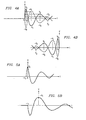
- FIGURE 4A is a plot of an exemplary shifting of standard voltage response to construct the stimulus input according to the teachings of the present invention.
- FIGURE 4B is a plot of an exemplary system response waveform in reverse time order
- FIGURES 5A through 5D are plots of exemplary shifted voltage responses by t i or t j according to the teachings of the present invention.
- FIGURE 6 is a plot of an exemplary input stimulus current operable to induce a worst-case voltage response according to the teachings of the present invention
- FIGURE 7 is a plot of an exemplary stimulus current and inverse standard stimulus current according to the teachings of the present invention.
- FIGURE 8 is a plot of an exemplary standard voltage response and inverse standard voltage response according to the teachings of the present invention.
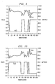
- FIGURE 9 is a plot of an exemplary worst case minimum voltage and stimulus current according to the teachings of the present invention.
- FIGURE 10 is a plot of an exemplary worst-case maximum voltage and stimulus current according to the teachings of the present invention.
- FIGURES 1 through 10 of the drawings like numerals being used for like and corresponding parts of the various drawings.
- FIGURE 1 is a simplified block diagram illustrating an embodiment of the present invention.
- the present invention is applicable to mechanical or electrical systems.
- a system 10 receives an input as a function of time, such as I(t).
- the input may be unevenness in the road for an automotive suspension system, for example, or the input current of an electrical/electronic circuit such as a microprocessor.
- the output or system response to the input as a function of time is V(t). It is of interest to system designers to determine whether system 10 is able to function properly when it is subjected to an input that subjects system 10 to the maximum excitation.
- FIGURE 2 is a flowchart of an embodiment of a method 12 of determining the input that would create the maximum system response according to the teachings of the present invention.
- System 10 is first subject to a step input.
- FIGURE 3 is an exemplary plot of a step current function having a high current level at t ⁇ 0 and at a low current level at t > 0.
- this input may be some standard input or excitation that would generate a measurable system response. Note that there is some finite time during which the time the current level transitions from high to low levels.
- FIGURE 3 further shows a voltage step response to the input current. The points in time, t 0 , t 1 , t 2 , t 3 ,...,where local maxima (V 0 and V 2 , for example, as shown in FIGURE 3) and minima (V 1 and V 3 , for example) responses occur are noted, as shown in blocks 14 and 16 of FIGURE 2. The maxima and minima time occurrences are noted until V(t) tapers to insignificant or unimportant measurements. The occurrences of the maximum points should alternate with the minimum points. In other words, there is only one maximum between any two adjacent minimum points, and there is only one minimum between any two adjacent maximum points.
- a time, T is chosen that is equal or later in time than the maximum of time points t 0 , t 1 , t 2 , t 3 ,....
- the worst-case stimuli is defined as the input that results in maximum or minimum response value.
- the positive and negative voltage step responses can be shifted by shifting the positive and negative input current transients so. that the worst-case voltage response occurs at T, as seen in FIGURE 4.
- a shift of the voltage step response by -to is made, and an input at the maximum input value is determined, as shown in FIGURE 5A.
- FIGURE 5B a shift of the negative or inverse voltage step response by -t 1 is made.
- FIGURE 5C a shift of the voltage step response by -t 2 is made.
- FIGURE 5D a shift of the negative voltage step response by -t 3 is made.
- FIGURE 5E shows a composite plot of all the shifted voltage step response and negative voltage step responses. At time T, the worst-case system response would occur.
- FIGURE 7 a plot of an exemplary standard stimulus current and inverse standard stimulus current plotted by a circuit simulation software.
- FIGURE 8 is a plot of an exemplary standard voltage response and inverse standard voltage response, V(t).
- FIGURE 9 is a plot of an exemplary worst case minimum voltage and stimulus current according to the teachings of the present invention, and
- FIGURE 10 is a plot of an exemplary worst case maximum voltage and stimulus current according to the teachings of the present invention.
- the method of the present invention is operable to determine the input excitation that would induce the maximum and minimum response in the target system. In test conditions the stimulus input is maintained within its maximum and minimum bounds while the waveform is random.
- the present invention has been described with respect to electrical or electronic systems, the present invention is also applicable to mechanical systems such as automotive suspension systems, for example, where it is of interest to subject the system to an input that would create the worst-case response to verify the system design and operations.
- the unit step input for a suspension system may be a bump of a predetermined height, such as five inches.
- the system response would be the amount of deviation from neutral in the upward and downward directions, and the times t i for maximum deviation in the upward direction and times t j for maximum deviation in the downward direction. It may be seen that the present invention may be modified and adapted to the testing and modeling of other types of systems either in a laboratory or in a simulated model.
- the present invention may be embodied in a test system or simulation system that first determines the worst-case excitation input of the target system, and then subjects the target system to the worst-case excitation input. Again, the system may test the actual system or simulate the testing with a model of the system.
- a test system or simulation system that first determines the worst-case excitation input of the target system, and then subjects the target system to the worst-case excitation input.
- the system may test the actual system or simulate the testing with a model of the system.
- Such a system is likely to be microprocessor-based and have an interface that is operable to supply the excitation input to the system being tested and to receive output from the system.
Landscapes
- Engineering & Computer Science (AREA)
- Computer Hardware Design (AREA)
- Theoretical Computer Science (AREA)
- Physics & Mathematics (AREA)
- General Engineering & Computer Science (AREA)
- General Physics & Mathematics (AREA)
- Geometry (AREA)
- Evolutionary Computation (AREA)
- Microelectronics & Electronic Packaging (AREA)
- Quality & Reliability (AREA)
- Tests Of Electronic Circuits (AREA)
- Test And Diagnosis Of Digital Computers (AREA)
- Management, Administration, Business Operations System, And Electronic Commerce (AREA)
- Vehicle Body Suspensions (AREA)
Abstract
Description
- The present invention relates generally to the field of system analysis, and in particular a system and method of system response testing and modeling.
- When a system design is under analysis, it is of interest to determine the profile of an input to the system that would lead to the worst-case excitation or response. When the system is under maximum stress, the system behavior can be studied and any undesirable system response can be remedied by design modifications. Systems that can benefit from this analysis include mechanical systems such as automotive suspension system, as well as electronic circuits and systems such as microprocessors.
- The ever-increasing clock frequencies and power requirements of microprocessors is putting more demands on the power distribution system. It is critically important that the power distribution system is able to supply the large current demands of the microprocessor at a voltage fixed within certain tolerances. Since the amount of current the microprocessor requires changes in time, both within the period of the microprocessor clock and over many clock cycles, the traditional method for analyzing, modeling and testing the power distribution system has been focused on measuring impedance as a function of frequency. However, focusing on the frequency domain behavior of the power distribution system does not factor in the actual voltage profile of the microprocessor. Such information may be extremely helpful.
- In accordance with an embodiment of the present invention, a method comprises exciting a system with a step input having predetermined maximum and minimum input values, selecting time points ti and tj in a system response having a plurality of maximum response values at time points ti and a plurality of minimum response values at time points tj. A maximum worst-case excitation input is then generated. The maximum worst-case excitation input has a positive transition from the predetermined minimum input value to the predetermined maximum input value at each time point (T - ti), and a negative transition from the predetermined maximum input value to the predetermined minimum input value at each time point (T - tj).
- In accordance with another embodiment of the invention, a method comprises exciting a system with a worst-case excitation input. The worst-case excitation input is generated by selecting time points ti and tj in a standard system response to a standard input having a plurality of maximum response values at time points ti and a plurality of minimum response values at time points tj, the standard input having predetermined minimum and maximum input values. A maximum worst-case excitation input is generated, which has a positive transition from the predetermined minimum input value to the predetermined maximum input value at each time (T - ti), and a negative transition from the predetermined maximum input value to the predetermined minimum input value at each time (T - tj). A worst-case system response to the worst-case excitation input is then observed.
- In accordance with yet another embodiment of the present invention, a system comprises an interface to a target system, the interface operable to supply input to the target system and receive output from the target system, and a microprocessor coupled to the interface and operable to generate a worst-case excitation input. The worst-case excitation input is generated by: selecting time points ti and tj in a standard system response to a standard input having a plurality of maximum response values at time points ti and a plurality of minimum response values at time points tj, the standard input having predetermined minimum and maximum input values, and generating a maximum worst-case excitation waveform having a positive transition from the predetermined minimum input value to the predetermined maximum input value at each time (T - ti), and a negative transition from the predetermined maximum input value to the predetermined minimum input value at each time (T - tj).
- In accordance with another embodiment of the present invention, a system comprising a computer-executable medium having encoded thereon a process is provided. The process is operable to excite a system with a step input having predetermined maximum and minimum input values, select time points ti and tj in a system response having a plurality of maximum response values at time points ti and a plurality of minimum response values at time points tj, and generate a maximum worst-case excitation input having a positive transition from the predetermined minimum input value to the predetermined maximum input value at each time point (T - ti), and a negative transition from the predetermined maximum input value to the predetermined minimum input value at each time point (T - tj).
- For a more complete understanding of the present invention, the objects and advantages thereof, reference is now made to the following descriptions taken in connection with the accompanying drawings in which:
- FIGURE 1 is a simplified block diagram illustrating an embodiment of the present invention;
- FIGURE 2 is a flowchart of an embodiment of a method of determining the maximum system response according to the teachings of the present invention;
- FIGURES 3A and 3B are a plots of an exemplary stimulus current and standard voltage response, respectively, according to the teachings of the present invention;
- FIGURE 4A is a plot of an exemplary shifting of standard voltage response to construct the stimulus input according to the teachings of the present invention;
- FIGURE 4B is a plot of an exemplary system response waveform in reverse time order;
- FIGURES 5A through 5D are plots of exemplary shifted voltage responses by ti or tj according to the teachings of the present invention;
- FIGURE 6 is a plot of an exemplary input stimulus current operable to induce a worst-case voltage response according to the teachings of the present invention;
- FIGURE 7 is a plot of an exemplary stimulus current and inverse standard stimulus current according to the teachings of the present invention;
- FIGURE 8 is a plot of an exemplary standard voltage response and inverse standard voltage response according to the teachings of the present invention;
- FIGURE 9 is a plot of an exemplary worst case minimum voltage and stimulus current according to the teachings of the present invention; and
- FIGURE 10 is a plot of an exemplary worst-case maximum voltage and stimulus current according to the teachings of the present invention.
- The preferred embodiment of the present invention and its advantages are best understood by referring to FIGURES 1 through 10 of the drawings, like numerals being used for like and corresponding parts of the various drawings.
- FIGURE 1 is a simplified block diagram illustrating an embodiment of the present invention. The present invention is applicable to mechanical or electrical systems. A
system 10 receives an input as a function of time, such as I(t). Depending on the type of system, the input may be unevenness in the road for an automotive suspension system, for example, or the input current of an electrical/electronic circuit such as a microprocessor. The output or system response to the input as a function of time is V(t). It is of interest to system designers to determine whethersystem 10 is able to function properly when it is subjected to an input thatsubjects system 10 to the maximum excitation. - FIGURE 2 is a flowchart of an embodiment of a
method 12 of determining the input that would create the maximum system response according to the teachings of the present invention.System 10 is first subject to a step input. FIGURE 3 is an exemplary plot of a step current function having a high current level at t < 0 and at a low current level at t > 0. For mechanical systems, this input may be some standard input or excitation that would generate a measurable system response. Note that there is some finite time during which the time the current level transitions from high to low levels. If the step function is a unit step function, it can be expressed as:

blocks - In
block 18, a time, T, is chosen that is equal or later in time than the maximum of time points t0, t1, t2, t3,.... The quantities (T - t0), (T - t1), (T - t2), (T - t3),...are then computed. Because T is greater than the maximum and minimum time points, these quantities are positive. T will be the point in time that is chosen for the occurrence of the worst-case response. The worst-case stimuli is defined as the input that results in maximum or minimum response value. To obtain the stimulus for maximum response value of the system at time moment T, all positive transitions from low-to-high levels of the input at all such time moments (T - ti) are set such that the points ti are the points of maximum for the transient response. The negative transitions from high-to-low levels of the input are also set for all such time moments (T - tj). Points tj are the points in time where the local minima occur. To obtain the stimulus for minimum response value of the system at time moment T, all negative transitions from high to low levels of the input at all such time moments (T - ti) are set such that the points ti are the points of maximum for the transient response. The positive transitions from low to high levels of the input at time (T - tj) are set such that tj are points of minimum. These two steps are shown inblocks - Therefore, the positive and negative voltage step responses can be shifted by shifting the positive and negative input current transients so. that the worst-case voltage response occurs at T, as seen in FIGURE 4. In the example, because at to a low-to-high voltage response transition occurs, a shift of the voltage step response by -to is made, and an input at the maximum input value is determined, as shown in FIGURE 5A. In FIGURE 5B, a shift of the negative or inverse voltage step response by -t1 is made. In FIGURE 5C, a shift of the voltage step response by -t2 is made. In FIGURE 5D, a shift of the negative voltage step response by -t3 is made. FIGURE 5E shows a composite plot of all the shifted voltage step response and negative voltage step responses. At time T, the worst-case system response would occur.
- All maxima of the system response and all maxima of the inverse system response will be gathered by this special input waveform at the time moment T. Constructed in this manner, each positive transition starting at time moment (T - ti) will cause a maximum of the transient response exactly at the time moment T. Each negative transition will cause a maximum of the inverse transient response at the time moment T. All maxima of the system response and all maxima of the inverse system response are therefore accumulated at the time moment T. In effect, the system response is flipped with respect to the time axis so that the times used to build the worst case stimulus are in the reverse order of the points of maxima and minima of the system step response, as shown in FIGURE 4B. A plot illustrating an exemplary excitation input current that corresponds to the voltage response in FIGURES 3 through 5 is shown in FIGURE 6. It may be seen that all maximum and minimum points are shifted so that they occur at the chosen time T. Therefore, in this example,


- As shown in FIGURE 7, a plot of an exemplary standard stimulus current and inverse standard stimulus current plotted by a circuit simulation software. FIGURE 8 is a plot of an exemplary standard voltage response and inverse standard voltage response, V(t). FIGURE 9 is a plot of an exemplary worst case minimum voltage and stimulus current according to the teachings of the present invention, and FIGURE 10 is a plot of an exemplary worst case maximum voltage and stimulus current according to the teachings of the present invention.
- In conventional system testing and modeling, the typical choice of step function or meander wave with constant pulse repetition frequency do not induce the worst case system response. The method of the present invention is operable to determine the input excitation that would induce the maximum and minimum response in the target system. In test conditions the stimulus input is maintained within its maximum and minimum bounds while the waveform is random.
- Although the present invention has been described with respect to electrical or electronic systems, the present invention is also applicable to mechanical systems such as automotive suspension systems, for example, where it is of interest to subject the system to an input that would create the worst-case response to verify the system design and operations. For example, the unit step input for a suspension system may be a bump of a predetermined height, such as five inches. The system response would be the amount of deviation from neutral in the upward and downward directions, and the times ti for maximum deviation in the upward direction and times tj for maximum deviation in the downward direction. It may be seen that the present invention may be modified and adapted to the testing and modeling of other types of systems either in a laboratory or in a simulated model.
The present invention may be embodied in a test system or simulation system that first determines the worst-case excitation input of the target system, and then subjects the target system to the worst-case excitation input. Again, the system may test the actual system or simulate the testing with a model of the system. Such a system is likely to be microprocessor-based and have an interface that is operable to supply the excitation input to the system being tested and to receive output from the system.
Claims (10)
- A method (12), comprising:exciting a system (10) with a standard input having predetermined maximum and minimum input values (14);selecting time points ti and tj in a system response having a plurality of maximum response values at time points ti and a plurality of minimum response values at time points tj (16); andgenerating a maximum worst-case excitation input having a positive transition from the predetermined minimum input value to the predetermined maximum input value at each time point (T - ti), and a negative transition from the predetermined maximum input value to the predetermined minimum input value at each time point (T - tj) (18, 20).
- The method, as set forth in claim 1, further comprising generating a minimum worst-case excitation input having a negative transition from the predetermined minimum input value to the predetermined maximum input value at each time point (T - ti), and a positive transition from the predetermined maximum input value to the predetermined minimum input value at each time point (T - tj) (18, 22).
- The method, as set forth in claim 1, wherein exciting a system comprises exciting the system with a unit step current input (14).
- The method, as set forth in claim 1, wherein selecting time points comprises selecting any two adjacent maximum response values with a minimum response value therebetween.
- The method, as set forth in claim 2, further comprising exciting the system using at least one of the maximum and minimum worst-case excitation input.
- The method, as set forth in claim 2, further comprising exciting a simulation model of the system using at least one of the maximum and minimum worst-case excitation input.
- A system comprising:computer-executable medium having encoded therein a process operable to:excite a system with a step input having predetermined maximum and minimum input values (14);select time points ti and tj in a system response having a plurality of maximum response values at time points ti and a plurality of minimum response values at time points tj (16); andgenerate a maximum worst-case excitation input having a positive transition from the predetermined minimum input value to the predetermined maximum input value at each time point (T - ti), and a negative transition from the predetermined maximum input value to the predetermined minimum input value at each time point (T - tj) (18, 20).
- The system, as set forth in claim 7, wherein the process is further operable to generate a minimum worst-case excitation input having a negative transition from the predetermined minimum input value to the predetermined maximum input value at each time point (T - ti), and a positive transition from the predetermined maximum input value to the predetermined minimum input value at each time point (T - tj) (18, 22).
- The system, as set forth in claim 7, wherein the process is further operable to excite the system with a unit step current input (14).
- The system, as set forth in claim 7, wherein the process is further operable to select any two adjacent maximum response values with a minimum response value therebetween.
Applications Claiming Priority (2)
| Application Number | Priority Date | Filing Date | Title |
|---|---|---|---|
| US10/274,712 US20040078183A1 (en) | 2002-10-21 | 2002-10-21 | System and method of system response testing and modeling |
| US274712 | 2002-10-21 |
Publications (2)
| Publication Number | Publication Date |
|---|---|
| EP1413965A2 true EP1413965A2 (en) | 2004-04-28 |
| EP1413965A3 EP1413965A3 (en) | 2004-12-08 |
Family
ID=32069294
Family Applications (1)
| Application Number | Title | Priority Date | Filing Date |
|---|---|---|---|
| EP03256574A Withdrawn EP1413965A3 (en) | 2002-10-21 | 2003-10-17 | System response testing and modeling |
Country Status (6)
| Country | Link |
|---|---|
| US (1) | US20040078183A1 (en) |
| EP (1) | EP1413965A3 (en) |
| JP (1) | JP2004145882A (en) |
| KR (1) | KR20040034533A (en) |
| IL (1) | IL155929A (en) |
| TW (1) | TWI223198B (en) |
Cited By (1)
| Publication number | Priority date | Publication date | Assignee | Title |
|---|---|---|---|---|
| CN110096750A (en) * | 2019-04-02 | 2019-08-06 | 燕山大学 | Consider the adaptive dynamic surface control method of non-linear Active suspension actuator |
Family Cites Families (18)
| Publication number | Priority date | Publication date | Assignee | Title |
|---|---|---|---|---|
| US4924430A (en) * | 1988-01-28 | 1990-05-08 | Teradyne, Inc. | Static timing analysis of semiconductor digital circuits |
| JPH06276039A (en) * | 1993-03-17 | 1994-09-30 | Sanyo Electric Co Ltd | Method for designing high frequency circuit |
| JP3727103B2 (en) * | 1996-04-05 | 2005-12-14 | 三菱電機株式会社 | Test method for semiconductor devices |
| US6049219A (en) * | 1996-05-13 | 2000-04-11 | The United States Of America As Represented By The Secretary Of The Air Force | Signal probing of microwave integrated circuit internal nodes |
| US6185723B1 (en) * | 1996-11-27 | 2001-02-06 | International Business Machines Corporation | Method for performing timing analysis of a clock-shaping circuit |
| BR9909905B1 (en) * | 1998-04-03 | 2012-12-11 | operator for an overhead power switch and method of operating an overhead power switch. | |
| US6567773B1 (en) * | 1999-11-17 | 2003-05-20 | International Business Machines Corporation | Use of static noise analysis for integrated circuits fabricated in a silicon-on-insulator process technology |
| JP2001208803A (en) * | 2000-01-24 | 2001-08-03 | Advantest Corp | Failure simulation method and failure simulator for semiconductor integrated circuit |
| US6518782B1 (en) * | 2000-08-29 | 2003-02-11 | Delta Design, Inc. | Active power monitoring using externally located current sensors |
| JP2002110489A (en) * | 2000-09-26 | 2002-04-12 | Toshiba Corp | Simulator for circuit characteristics of semiconductor device and simulation method |
| US6442741B1 (en) * | 2000-10-06 | 2002-08-27 | Lsi Logic Corporation | Method of automatically generating schematic and waveform diagrams for analysis of timing margins and signal skews of relevant logic cells using input signal predictors and transition times |
| US6472899B2 (en) * | 2000-12-29 | 2002-10-29 | Intel Corporation | Method for determining a load line based variable voltage input for an integrated circuit product |
| US6665843B2 (en) * | 2001-01-20 | 2003-12-16 | International Business Machines Corporation | Method and system for quantifying the integrity of an on-chip power supply network |
| US6564365B1 (en) * | 2001-08-03 | 2003-05-13 | Hewlett-Packard Development Company, L.P. | Method of simultaneously displaying schematic and timing data |
| US7062734B2 (en) * | 2002-04-05 | 2006-06-13 | Collins Jr Truman Wesley | Slack time analysis through latches on a circuit design |
| US7840803B2 (en) * | 2002-04-16 | 2010-11-23 | Massachusetts Institute Of Technology | Authentication of integrated circuits |
| US7155691B2 (en) * | 2003-06-06 | 2006-12-26 | Nascentric, Inc. | Apparatus and methods for compiled static timing analysis |
| US7102357B2 (en) * | 2004-03-22 | 2006-09-05 | Hewlett-Packard Development Company, L.P. | Determination of worst case voltage in a power supply loop |
-
2002
- 2002-10-21 US US10/274,712 patent/US20040078183A1/en not_active Abandoned
-
2003
- 2003-05-15 IL IL155929A patent/IL155929A/en not_active IP Right Cessation
- 2003-05-20 TW TW092113582A patent/TWI223198B/en not_active IP Right Cessation
- 2003-10-09 JP JP2003350743A patent/JP2004145882A/en not_active Withdrawn
- 2003-10-17 EP EP03256574A patent/EP1413965A3/en not_active Withdrawn
- 2003-10-20 KR KR1020030072838A patent/KR20040034533A/en not_active Withdrawn
Cited By (2)
| Publication number | Priority date | Publication date | Assignee | Title |
|---|---|---|---|---|
| CN110096750A (en) * | 2019-04-02 | 2019-08-06 | 燕山大学 | Consider the adaptive dynamic surface control method of non-linear Active suspension actuator |
| CN110096750B (en) * | 2019-04-02 | 2020-12-11 | 燕山大学 | Adaptive Dynamic Surface Control Method Considering Nonlinear Active Suspension Actuators |
Also Published As
| Publication number | Publication date |
|---|---|
| JP2004145882A (en) | 2004-05-20 |
| KR20040034533A (en) | 2004-04-28 |
| US20040078183A1 (en) | 2004-04-22 |
| TWI223198B (en) | 2004-11-01 |
| IL155929A0 (en) | 2003-12-23 |
| IL155929A (en) | 2006-08-20 |
| TW200406706A (en) | 2004-05-01 |
| EP1413965A3 (en) | 2004-12-08 |
Similar Documents
| Publication | Publication Date | Title |
|---|---|---|
| EP3936877B1 (en) | Measurement instrument, measurement system, and signal processing method | |
| EP2345905A2 (en) | Battery characteristic evaluator | |
| US20040049750A1 (en) | Process and system for identifying wires at risk of electromigration | |
| US20040078175A1 (en) | Method and apparatus for modeling and simulating the effects of bridge defects in integrated circuits | |
| JP4500338B2 (en) | Test pattern evaluation method and test pattern evaluation apparatus | |
| US6795802B2 (en) | Apparatus and method for calculating temporal deterioration margin amount of LSI, and LSI inspection method | |
| US20050024064A1 (en) | System and method for testing devices | |
| EP1413965A2 (en) | System response testing and modeling | |
| EP0590575A1 (en) | Test control circuit for scan path | |
| US20080155484A1 (en) | System and method for memory element characterization | |
| US6934670B2 (en) | Virtual test environment | |
| JP4600823B2 (en) | Electronic circuit analysis program, method and apparatus | |
| CN114355161B (en) | Interconnection status online monitoring circuit and method | |
| Stievano et al. | Behavioral models of digital IC ports from measured transient waveforms | |
| US20060190872A1 (en) | System and method for signal integrity testing of electronic circuits | |
| Gunther | A proposed flicker meter test protocol | |
| JP4295894B2 (en) | Semiconductor device test apparatus and test method | |
| US20040002847A1 (en) | Method for creating and displaying signaling eye-plots | |
| EP3786651B1 (en) | Method and device for providing a behaviour model for simulating electromagnetic interference emissions of an electrical or electronic component | |
| JP2003030270A (en) | Method and device for verifying property of synchronous sequential circuit | |
| EP0853280A2 (en) | Timing verification method and device | |
| JP2624135B2 (en) | Timing analysis method | |
| CN119667438A (en) | A RISC-V DSP chip test waveform automatic generation method, system and storage medium | |
| JP3123982B2 (en) | Logic simulation method | |
| Doyle et al. | Techniques and considerations for verification of model causality |
Legal Events
| Date | Code | Title | Description |
|---|---|---|---|
| PUAI | Public reference made under article 153(3) epc to a published international application that has entered the european phase |
Free format text: ORIGINAL CODE: 0009012 |
|
| AK | Designated contracting states |
Kind code of ref document: A2 Designated state(s): AT BE BG CH CY CZ DE DK EE ES FI FR GB GR HU IE IT LI LU MC NL PT RO SE SI SK TR |
|
| AX | Request for extension of the european patent |
Extension state: AL LT LV MK |
|
| PUAL | Search report despatched |
Free format text: ORIGINAL CODE: 0009013 |
|
| AK | Designated contracting states |
Kind code of ref document: A3 Designated state(s): AT BE BG CH CY CZ DE DK EE ES FI FR GB GR HU IE IT LI LU MC NL PT RO SE SI SK TR |
|
| AX | Request for extension of the european patent |
Extension state: AL LT LV MK |
|
| 17P | Request for examination filed |
Effective date: 20050606 |
|
| AKX | Designation fees paid |
Designated state(s): DE FR GB IT |
|
| STAA | Information on the status of an ep patent application or granted ep patent |
Free format text: STATUS: THE APPLICATION IS DEEMED TO BE WITHDRAWN |
|
| 18D | Application deemed to be withdrawn |
Effective date: 20080503 |