EP1411589A2 - High-frequency transceiver apparatus and method of manufacturing the same - Google Patents
High-frequency transceiver apparatus and method of manufacturing the same Download PDFInfo
- Publication number
- EP1411589A2 EP1411589A2 EP03023689A EP03023689A EP1411589A2 EP 1411589 A2 EP1411589 A2 EP 1411589A2 EP 03023689 A EP03023689 A EP 03023689A EP 03023689 A EP03023689 A EP 03023689A EP 1411589 A2 EP1411589 A2 EP 1411589A2
- Authority
- EP
- European Patent Office
- Prior art keywords
- frequency
- transceiver apparatus
- base plate
- projection
- frequency transceiver
- Prior art date
- Legal status (The legal status is an assumption and is not a legal conclusion. Google has not performed a legal analysis and makes no representation as to the accuracy of the status listed.)
- Withdrawn
Links
Images


Classifications
-
- H—ELECTRICITY
- H01—ELECTRIC ELEMENTS
- H01Q—ANTENNAS, i.e. RADIO AERIALS
- H01Q1/00—Details of, or arrangements associated with, antennas
- H01Q1/27—Adaptation for use in or on movable bodies
- H01Q1/32—Adaptation for use in or on road or rail vehicles
- H01Q1/3208—Adaptation for use in or on road or rail vehicles characterised by the application wherein the antenna is used
- H01Q1/3233—Adaptation for use in or on road or rail vehicles characterised by the application wherein the antenna is used particular used as part of a sensor or in a security system, e.g. for automotive radar, navigation systems
-
- H—ELECTRICITY
- H01—ELECTRIC ELEMENTS
- H01Q—ANTENNAS, i.e. RADIO AERIALS
- H01Q21/00—Antenna arrays or systems
- H01Q21/0087—Apparatus or processes specially adapted for manufacturing antenna arrays
-
- H—ELECTRICITY
- H01—ELECTRIC ELEMENTS
- H01Q—ANTENNAS, i.e. RADIO AERIALS
- H01Q21/00—Antenna arrays or systems
- H01Q21/06—Arrays of individually energised antenna units similarly polarised and spaced apart
- H01Q21/061—Two dimensional planar arrays
- H01Q21/065—Patch antenna array
-
- H—ELECTRICITY
- H01—ELECTRIC ELEMENTS
- H01Q—ANTENNAS, i.e. RADIO AERIALS
- H01Q23/00—Antennas with active circuits or circuit elements integrated within them or attached to them
-
- G—PHYSICS
- G01—MEASURING; TESTING
- G01S—RADIO DIRECTION-FINDING; RADIO NAVIGATION; DETERMINING DISTANCE OR VELOCITY BY USE OF RADIO WAVES; LOCATING OR PRESENCE-DETECTING BY USE OF THE REFLECTION OR RERADIATION OF RADIO WAVES; ANALOGOUS ARRANGEMENTS USING OTHER WAVES
- G01S13/00—Systems using the reflection or reradiation of radio waves, e.g. radar systems; Analogous systems using reflection or reradiation of waves whose nature or wavelength is irrelevant or unspecified
- G01S13/88—Radar or analogous systems specially adapted for specific applications
- G01S13/93—Radar or analogous systems specially adapted for specific applications for anti-collision purposes
- G01S13/931—Radar or analogous systems specially adapted for specific applications for anti-collision purposes of land vehicles
- G01S2013/9327—Sensor installation details
- G01S2013/93271—Sensor installation details in the front of the vehicles
Definitions
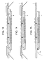
- an upper lid is previously provided with a cut hole for mounting the patch antenna thereon, so that a board having the patch antenna mounted thereon is bonded onto the cut hole.
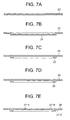
- Such a shaped product A 24 having the roughly-shaped projection 23 as shown in Fig. 7C is then subjected to third-stage shaping operation by such a press die 50 as shown in Fig. 10.
- the press die 50 is made up of a lower die part 51 as a fixed side and an upper die part 52 as a driving side.
- the lower die part 51 includes a die 53 which has a recess 54.
- the upper die part 52 is provided with a projection 55 which fits into the recess 54 of the lower die part 51.
- the shaped product B 26 of Fig. 7D having the projection 25 shaped with a good edge angle accuracy is finish-shaped by such a press die 60 as shown in Fig. 11.
- the press die 60 similarly to the press die 50, is made up of a lower die part 61 as a fixed side and an upper die part 62 as a driving side.
- the press die 60 is different from the press die 50. That is, the press die 60 is not a bending die but a punching die. That is, punches 63, which are provided to the upper die part 62, function to make holes in the shaped product B 26 at predetermined positions.
- the antenna mounting base (base plate) 1 is manufactured by methods other than the aforementioned method, including machining.
- the apparatus is smaller in productivity than the apparatus manufactured by the aforementioned pressing, but its processing accuracy is too high to be compared with that by pressing.
- the cover 5 has a cup shape, and the output line 12 is led out from the side surface of the cover 5.
- the high-frequency transceiver apparatus when used as a headway distance detecting apparatus (millimeter wave radar), its performance can be increased and its detection distance can be prolonged by securing the flatness accuracy of the patch antenna element. Further, when the antenna mounting base (base plate) is manufactured by pressing, its cost can be lowered and its performance can be enhanced.
Landscapes
- Engineering & Computer Science (AREA)
- Computer Security & Cryptography (AREA)
- Radar, Positioning & Navigation (AREA)
- Remote Sensing (AREA)
- Manufacturing & Machinery (AREA)
- Radar Systems Or Details Thereof (AREA)
- Variable-Direction Aerials And Aerial Arrays (AREA)
- Details Of Aerials (AREA)
- Waveguide Aerials (AREA)
Abstract
Description
Claims (14)
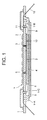
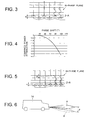
- A high-frequency transceiver apparatus (100), wherein an antenna substrate (2) made of a dielectric material and having an antenna conductor pattern (7) formed thereon is bonded onto one surface of a base plate (1) to transmit and receive a high frequency wave signal, and the flatness accuracy of a surface of said antenna substrate (2) is set at λ/20 or less when λ denotes effective wavelength.
- The high-frequency transceiver apparatus (100) as set forth in claim 1, wherein a high-frequency circuit substrate (3) made of a dielectric material and forming a transceiver circuit is provided on the other surface of said base plate.
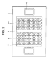
- The high-frequency transceiver apparatus as set forth in claim 2, wherein said transceiver circuit includes a circuit conductor pattern formed on the surface of said high-frequency circuit substrate (3) and a semiconductor chip (4) connected to said circuit conductor pattern (10), and said antenna conductor pattern is arranged as connected with a plurality of patch antenna elements (2-A).
- The high-frequency transceiver apparatus as set forth in claim 2 or 3, wherein said antenna substrate (7) and said high-frequency circuit substrate (3) are integrally formed for transmission and reception.
- The high-frequency transceiver apparatus as set forth in claim 3 or 4, wherein a cover (5) having a radio wave absorber (8) is mounted on a surface of said base plate having the high-frequency circuit substrate mounted thereon.
- The high-frequency transceiver apparatus as set forth in claim 5, wherein a projection (1-A) is formed in the other surface of said base plate so as to surround a periphery of the high-frequency circuit substrate (3), and said cover having said radio wave absorber (8) is mounted on an upper face of said projection.
- The high-frequency transceiver apparatus as set forth in claim 1, 2, 3, 4, 5 or 6, wherein an effective wavelength frequency is any frequency in a range from 76 to 77GHz.
- The high-frequency transceiver apparatus as set forth in claim 3, 4, 5, 6 or 7, wherein said semiconductor chip (4) is made of a compound of Ga and As, and said high-frequency circuit substrate (3) is air-tightly sealed by joining the cover (5) thereto.
- The high-frequency transceiver apparatus as set forth in claim 1, 2, 3, 4, 5, 6, 7 or 8, wherein said base plate (1) is formed by press processing.
- The high-frequency transceiver apparatus as set forth in claim 9, wherein a surface of said base plate (1) onto which said antenna substrate (2) is to be bonded is subjected to annealing operation to remove distortion.
- The high-frequency transceiver apparatus as set forth in claim 6, wherein said base plate is manufactured by shaping a metallic plate work into a plate having dimensions corresponding nearly to an outer periphery of the projection, shaping said shaped plate into a plate having dimensions corresponding nearly to an inner periphery of said projection inside the projection, annealing said shaped plate to remove distortion, and then shaping the cover mounting face of said projection.
- A high-frequency transceiver apparatus (100) to be mounted on a car, wherein an antenna substrate (2) having an antenna conductor pattern (7) formed thereon as connected with a plurality of patch antenna elements (2-A) is bonded onto one surface of a base plate (1), a high-frequency circuit substrate (3) including a circuit conductor pattern (10) and a semiconductor chip (4) connected to said circuit conductor pattern is provided on the other surface of said base plate, said antenna substrate (2) and said high-frequency circuit substrate are integrally formed for transmission and reception, a projection (1-A) is formed on the other surface of said base plate so as to surround said high-frequency circuit substrate, a cover (5) having a radio wave absorber (8) is mounted on an upper face of said projection, said high-frequency transceiver apparatus for transmitting and receiving a high frequency wave signal is used for the purpose of detecting a distance between cars, and a flatness accuracy of a surface of said antenna substrate of the high-frequency transceiver apparatus is set at λ/20 or less when λ denotes effective wavelength, and an effective frequency of the high-frequency transceiver apparatus is set at any frequency in a range from 76 to 77GHz.
- The high-frequency transceiver apparatus as set forth in claim 12, wherein said base plate is formed by press processing.
- The high-frequency transceiver apparatus as set forth in claim 12 or 14, wherein said base plate is manufactured by shaping a metallic plate work into a plate having dimensions corresponding nearly to an outer periphery of the projection, shaping said shaped plate into a plate having dimensions corresponding nearly to an inner periphery of said projection inside the projection, annealing said shaped plate to remove distortion, and then shaping the cover mounting face of said projection.
Applications Claiming Priority (2)
| Application Number | Priority Date | Filing Date | Title |
|---|---|---|---|
| JP2002303897A JP2004140632A (en) | 2002-10-18 | 2002-10-18 | High frequency transmitting / receiving device and method of manufacturing the same |
| JP2002303897 | 2002-10-18 |
Publications (2)
| Publication Number | Publication Date |
|---|---|
| EP1411589A2 true EP1411589A2 (en) | 2004-04-21 |
| EP1411589A3 EP1411589A3 (en) | 2005-03-23 |
Family
ID=32040850
Family Applications (1)
| Application Number | Title | Priority Date | Filing Date |
|---|---|---|---|
| EP03023689A Withdrawn EP1411589A3 (en) | 2002-10-18 | 2003-10-17 | High-frequency transceiver apparatus and method of manufacturing the same |
Country Status (3)
| Country | Link |
|---|---|
| US (1) | US20050014539A1 (en) |
| EP (1) | EP1411589A3 (en) |
| JP (1) | JP2004140632A (en) |
Cited By (3)
| Publication number | Priority date | Publication date | Assignee | Title |
|---|---|---|---|---|
| WO2022088714A1 (en) * | 2020-10-30 | 2022-05-05 | 京东方科技集团股份有限公司 | Antenna and communication system |
| CN115224485A (en) * | 2021-04-15 | 2022-10-21 | 华为技术有限公司 | Detection device, antenna housing, millimeter wave radar and terminal equipment |
| US12531349B2 (en) | 2023-04-07 | 2026-01-20 | Beijing Boe Sensor Technology Co., Ltd. | Antenna and electronic device |
Families Citing this family (4)
| Publication number | Priority date | Publication date | Assignee | Title |
|---|---|---|---|---|
| JP5018168B2 (en) * | 2007-03-26 | 2012-09-05 | 三菱電機株式会社 | Antenna device |
| DE102012022960B4 (en) * | 2012-11-23 | 2021-12-30 | Schott Ag | Housing component, in particular for an electronics housing, and method for producing a housing component |
| JP6905438B2 (en) * | 2017-09-22 | 2021-07-21 | 株式会社フジクラ | Wireless communication module |
| EP3588673B1 (en) * | 2018-06-29 | 2024-04-03 | Advanced Automotive Antennas, S.L. | Under-roof antenna modules for vehicles |
Family Cites Families (4)
| Publication number | Priority date | Publication date | Assignee | Title |
|---|---|---|---|---|
| JP3471617B2 (en) * | 1997-09-30 | 2003-12-02 | 三菱電機株式会社 | Planar antenna device |
| US6809688B2 (en) * | 2000-06-30 | 2004-10-26 | Sharp Kabushiki Kaisha | Radio communication device with integrated antenna, transmitter, and receiver |
| US20020149107A1 (en) * | 2001-02-02 | 2002-10-17 | Avery Dennison Corporation | Method of making a flexible substrate containing self-assembling microstructures |
| JP3941416B2 (en) * | 2001-04-26 | 2007-07-04 | ソニー株式会社 | High frequency module device and manufacturing method thereof |
-
2002
- 2002-10-18 JP JP2002303897A patent/JP2004140632A/en active Pending
-
2003
- 2003-10-17 US US10/686,703 patent/US20050014539A1/en not_active Abandoned
- 2003-10-17 EP EP03023689A patent/EP1411589A3/en not_active Withdrawn
Cited By (3)
| Publication number | Priority date | Publication date | Assignee | Title |
|---|---|---|---|---|
| WO2022088714A1 (en) * | 2020-10-30 | 2022-05-05 | 京东方科技集团股份有限公司 | Antenna and communication system |
| CN115224485A (en) * | 2021-04-15 | 2022-10-21 | 华为技术有限公司 | Detection device, antenna housing, millimeter wave radar and terminal equipment |
| US12531349B2 (en) | 2023-04-07 | 2026-01-20 | Beijing Boe Sensor Technology Co., Ltd. | Antenna and electronic device |
Also Published As
| Publication number | Publication date |
|---|---|
| EP1411589A3 (en) | 2005-03-23 |
| JP2004140632A (en) | 2004-05-13 |
| US20050014539A1 (en) | 2005-01-20 |
Similar Documents
| Publication | Publication Date | Title |
|---|---|---|
| JP7303815B2 (en) | Radar system for vehicle perimeter detection with synthetic resin antenna | |
| Hasch et al. | Millimeter-wave technology for automotive radar sensors in the 77 GHz frequency band | |
| US7154432B2 (en) | Radar sensor | |
| US11277902B2 (en) | Single layer radio frequency integrated circuit package and related low loss grounded coplanar transmission line | |
| US9525206B2 (en) | Antenna unit, radar device, and composite sensor device | |
| CN102823062B (en) | Integrated Transceiver Antenna for Built-in Radar | |
| JP3964873B2 (en) | In-vehicle millimeter wave radar system | |
| CN102414574B (en) | Radar device and antenna device | |
| JP3302848B2 (en) | In-vehicle radar device | |
| EP1777551A2 (en) | Millimeter-wave radar apparatus and millimeter radar system | |
| CN102565782A (en) | Automotive radar system and method for using same | |
| US12313735B2 (en) | Radar sensor, motor vehicle, and method for operating a radar sensor | |
| JP2010256327A (en) | Dual-band antenna array and RF front end for millimeter-wave imagers and radar | |
| WO2005055366A1 (en) | Vehicle-mounted radar | |
| WO2006049877A2 (en) | Tapered slot feed for an automotive radar ant | |
| Schnabel et al. | Reflection, refraction, and self-jamming | |
| US7321338B2 (en) | On-board antenna | |
| EP1411589A2 (en) | High-frequency transceiver apparatus and method of manufacturing the same | |
| CN118632775A (en) | Coated automotive glass window with integrated radar unit | |
| US7671806B2 (en) | Antenna system for a radar transceiver | |
| CN115902859A (en) | radar system | |
| CN109428175B (en) | Antenna components, in-vehicle radar and automotive | |
| US20240210521A1 (en) | Radar device and method for producing a radar device | |
| CN110474164A (en) | A kind of vehicle-mounted millimeter wave broad-band chip integrated waveguide slot antenna | |
| CN210296625U (en) | A vehicle-mounted millimeter-wave broadband substrate integrated waveguide slot antenna |
Legal Events
| Date | Code | Title | Description |
|---|---|---|---|
| PUAI | Public reference made under article 153(3) epc to a published international application that has entered the european phase |
Free format text: ORIGINAL CODE: 0009012 |
|
| AK | Designated contracting states |
Kind code of ref document: A2 Designated state(s): AT BE BG CH CY CZ DE DK EE ES FI FR GB GR HU IE IT LI LU MC NL PT RO SE SI SK TR |
|
| AX | Request for extension of the european patent |
Extension state: AL LT LV MK |
|
| PUAL | Search report despatched |
Free format text: ORIGINAL CODE: 0009013 |
|
| AK | Designated contracting states |
Kind code of ref document: A3 Designated state(s): AT BE BG CH CY CZ DE DK EE ES FI FR GB GR HU IE IT LI LU MC NL PT RO SE SI SK TR |
|
| AX | Request for extension of the european patent |
Extension state: AL LT LV MK |
|
| RIN1 | Information on inventor provided before grant (corrected) |
Inventor name: MATSUURA, KAZUO Inventor name: KAWAHARA, KEIJI Inventor name: KOSHIZAKA, ATSUSHI |
|
| 17P | Request for examination filed |
Effective date: 20050714 |
|
| AKX | Designation fees paid |
Designated state(s): DE FR |
|
| STAA | Information on the status of an ep patent application or granted ep patent |
Free format text: STATUS: THE APPLICATION IS DEEMED TO BE WITHDRAWN |
|
| 18D | Application deemed to be withdrawn |
Effective date: 20060808 |