EP1411548A2 - Providing high precision resistance in an integrated circuit using a thin film resistor of controlled dimension - Google Patents
Providing high precision resistance in an integrated circuit using a thin film resistor of controlled dimension Download PDFInfo
- Publication number
- EP1411548A2 EP1411548A2 EP03103821A EP03103821A EP1411548A2 EP 1411548 A2 EP1411548 A2 EP 1411548A2 EP 03103821 A EP03103821 A EP 03103821A EP 03103821 A EP03103821 A EP 03103821A EP 1411548 A2 EP1411548 A2 EP 1411548A2
- Authority
- EP
- European Patent Office
- Prior art keywords
- thin film
- film resistor
- stencil structure
- channel
- mask material
- Prior art date
- Legal status (The legal status is an assumption and is not a legal conclusion. Google has not performed a legal analysis and makes no representation as to the accuracy of the status listed.)
- Withdrawn
Links
- 239000010409 thin film Substances 0.000 title claims abstract description 164
- 239000000463 material Substances 0.000 claims abstract description 190
- 238000000034 method Methods 0.000 claims abstract description 57
- 239000000758 substrate Substances 0.000 claims abstract description 26
- 239000004020 conductor Substances 0.000 claims abstract description 12
- 230000009467 reduction Effects 0.000 claims abstract description 12
- 239000003989 dielectric material Substances 0.000 claims description 13
- 238000000151 deposition Methods 0.000 claims description 9
- 238000005530 etching Methods 0.000 claims description 7
- XAGFODPZIPBFFR-UHFFFAOYSA-N aluminium Chemical compound [Al] XAGFODPZIPBFFR-UHFFFAOYSA-N 0.000 claims description 4
- 229910052782 aluminium Inorganic materials 0.000 claims description 4
- 229920002120 photoresistant polymer Polymers 0.000 claims description 4
- RYGMFSIKBFXOCR-UHFFFAOYSA-N Copper Chemical compound [Cu] RYGMFSIKBFXOCR-UHFFFAOYSA-N 0.000 claims description 3
- 229910000599 Cr alloy Inorganic materials 0.000 claims description 3
- 229910000990 Ni alloy Inorganic materials 0.000 claims description 3
- 239000010949 copper Substances 0.000 claims description 3
- 229910052802 copper Inorganic materials 0.000 claims description 3
- VYZAMTAEIAYCRO-UHFFFAOYSA-N Chromium Chemical compound [Cr] VYZAMTAEIAYCRO-UHFFFAOYSA-N 0.000 claims description 2
- 239000004642 Polyimide Substances 0.000 claims description 2
- 229910001069 Ti alloy Inorganic materials 0.000 claims description 2
- 229910001080 W alloy Inorganic materials 0.000 claims description 2
- 239000011651 chromium Substances 0.000 claims description 2
- 238000009792 diffusion process Methods 0.000 claims description 2
- 239000011368 organic material Substances 0.000 claims description 2
- 229920001721 polyimide Polymers 0.000 claims description 2
- WFKWXMTUELFFGS-UHFFFAOYSA-N tungsten Chemical compound [W] WFKWXMTUELFFGS-UHFFFAOYSA-N 0.000 claims description 2
- 239000010937 tungsten Substances 0.000 claims description 2
- 230000004888 barrier function Effects 0.000 claims 1
- 239000010410 layer Substances 0.000 description 38
- 238000001039 wet etching Methods 0.000 description 12
- 230000008569 process Effects 0.000 description 9
- VYPSYNLAJGMNEJ-UHFFFAOYSA-N Silicium dioxide Chemical compound O=[Si]=O VYPSYNLAJGMNEJ-UHFFFAOYSA-N 0.000 description 8
- 230000003247 decreasing effect Effects 0.000 description 5
- KRHYYFGTRYWZRS-UHFFFAOYSA-N Fluorane Chemical compound F KRHYYFGTRYWZRS-UHFFFAOYSA-N 0.000 description 4
- 238000004380 ashing Methods 0.000 description 4
- 238000004519 manufacturing process Methods 0.000 description 4
- 235000012239 silicon dioxide Nutrition 0.000 description 4
- 239000000377 silicon dioxide Substances 0.000 description 4
- 230000015572 biosynthetic process Effects 0.000 description 3
- 238000007796 conventional method Methods 0.000 description 3
- 230000000873 masking effect Effects 0.000 description 3
- 238000000059 patterning Methods 0.000 description 3
- PXHVJJICTQNCMI-UHFFFAOYSA-N Nickel Chemical compound [Ni] PXHVJJICTQNCMI-UHFFFAOYSA-N 0.000 description 2
- BOTDANWDWHJENH-UHFFFAOYSA-N Tetraethyl orthosilicate Chemical compound CCO[Si](OCC)(OCC)OCC BOTDANWDWHJENH-UHFFFAOYSA-N 0.000 description 2
- 230000004075 alteration Effects 0.000 description 2
- 238000001312 dry etching Methods 0.000 description 2
- 238000012986 modification Methods 0.000 description 2
- 230000004048 modification Effects 0.000 description 2
- 150000004767 nitrides Chemical class 0.000 description 2
- 239000011241 protective layer Substances 0.000 description 2
- 239000005368 silicate glass Substances 0.000 description 2
- 238000006467 substitution reaction Methods 0.000 description 2
- 238000009966 trimming Methods 0.000 description 2
- BPQQTUXANYXVAA-UHFFFAOYSA-N Orthosilicate Chemical compound [O-][Si]([O-])([O-])[O-] BPQQTUXANYXVAA-UHFFFAOYSA-N 0.000 description 1
- 239000002253 acid Substances 0.000 description 1
- 229910045601 alloy Inorganic materials 0.000 description 1
- 239000000956 alloy Substances 0.000 description 1
- 238000006243 chemical reaction Methods 0.000 description 1
- 239000000788 chromium alloy Substances 0.000 description 1
- VNNRSPGTAMTISX-UHFFFAOYSA-N chromium nickel Chemical compound [Cr].[Ni] VNNRSPGTAMTISX-UHFFFAOYSA-N 0.000 description 1
- 230000008021 deposition Effects 0.000 description 1
- 239000011521 glass Substances 0.000 description 1
- BHEPBYXIRTUNPN-UHFFFAOYSA-N hydridophosphorus(.) (triplet) Chemical compound [PH] BHEPBYXIRTUNPN-UHFFFAOYSA-N 0.000 description 1
- 229910001120 nichrome Inorganic materials 0.000 description 1
- 238000005498 polishing Methods 0.000 description 1
- 229910052710 silicon Inorganic materials 0.000 description 1
- 239000010703 silicon Substances 0.000 description 1
- 239000002356 single layer Substances 0.000 description 1
- 239000002904 solvent Substances 0.000 description 1
- 239000000126 substance Substances 0.000 description 1
- 238000003631 wet chemical etching Methods 0.000 description 1
Images




Classifications
-
- H—ELECTRICITY
- H10—SEMICONDUCTOR DEVICES; ELECTRIC SOLID-STATE DEVICES NOT OTHERWISE PROVIDED FOR
- H10D—INORGANIC ELECTRIC SEMICONDUCTOR DEVICES
- H10D84/00—Integrated devices formed in or on semiconductor substrates that comprise only semiconducting layers, e.g. on Si wafers or on GaAs-on-Si wafers
- H10D84/201—Integrated devices formed in or on semiconductor substrates that comprise only semiconducting layers, e.g. on Si wafers or on GaAs-on-Si wafers characterised by the integration of only components covered by H10D1/00 or H10D8/00, e.g. RLC circuits
- H10D84/204—Integrated devices formed in or on semiconductor substrates that comprise only semiconducting layers, e.g. on Si wafers or on GaAs-on-Si wafers characterised by the integration of only components covered by H10D1/00 or H10D8/00, e.g. RLC circuits of combinations of diodes or capacitors or resistors
- H10D84/209—Integrated devices formed in or on semiconductor substrates that comprise only semiconducting layers, e.g. on Si wafers or on GaAs-on-Si wafers characterised by the integration of only components covered by H10D1/00 or H10D8/00, e.g. RLC circuits of combinations of diodes or capacitors or resistors of only resistors
-
- H—ELECTRICITY
- H10—SEMICONDUCTOR DEVICES; ELECTRIC SOLID-STATE DEVICES NOT OTHERWISE PROVIDED FOR
- H10D—INORGANIC ELECTRIC SEMICONDUCTOR DEVICES
- H10D1/00—Resistors, capacitors or inductors
- H10D1/40—Resistors
- H10D1/47—Resistors having no potential barriers
- H10D1/474—Resistors having no potential barriers comprising refractory metals, transition metals, noble metals, metal compounds or metal alloys, e.g. silicides
Definitions
- This invention relates generally to integrated circuits, and more particularly to providing high precision resistance in an integrated circuit using a thin film resistor of controlled dimension.
- Thin film resistors are often used in precision analog-to-digital and digital-to-analog integrated circuits for precision data conversion, which may require precise control of the resistance of the thin film resistor over the operating temperatures. Often the final fine control of the resistance of these precision thin film resistors must be done using laser trimming.
- a low resistivity material may be required to, for example: reduce the resistive-capacitive (RC)-time constant of the integrated circuit; minimize the thickness of the thin film resistor for ease of laser trimming; and reduce the integrated circuit area for low cost.
- a widely used thin film resistor may be formed, for example, from a deposited layer of nickel and chromium alloy and defined using wet chemical etching to remove unwanted thin film resistor material.
- wet etching techniques are used because currently the thin film resistor material may not be removable using dry etching techniques suitable for large-scale manufacturing of integrated circuits.
- wet etching techniques may suffer from dimension control problems such as etch-back or undercutting of the thin film resistor body, resulting in undesirable width reduction and variation in overall width of the thin film resistor body.
- the width of the thin film resistor can substantially affect the resistance of the thin film resistor, such dimension control problems may impair the ability to construct thin film resistors having a precise resistance and may result in yield losses during manufacturing of precision integrated analog circuits incorporating such thin film resistors.
- an integrated circuit includes a thin film resistor, which includes a resistor material that has been deposited on a substrate surface within a channel defined by opposing first and second portions of a stencil structure formed on the substrate surface, the resistor material having an initial width determined by a width of the channel.
- the stencil structure has been adapted to receive a planarizing material that protects against reduction of the initial width of the resistor material during subsequent process steps for removing the stencil structure.
- a head mask overlays an end portion of the thin film resistor and a dielectric overlays the head mask, the dielectric defining a via formed in the dielectric above a portion of the head mask.
- a conductive material has been deposited in the via, coupled to the portion of the head mask and electrically connecting the thin film resistor to other components of the integrated circuit.
- Particular embodiments of the present invention may provide one or more technical advantages. For example, certain embodiments may provide the ability to more uniformly and precisely control the width of the thin film resistor relative to previous techniques. The etch-back or undercutting of the thin film resistor associated with wet etching may be significantly reduced or eliminated completely, resulting in decreased width reduction and decreased variation in the overall width of the thin film resistor. In certain embodiments, for example, the thin film resistor has a final width of less than approximately 2 ⁇ m and the minimum width reduction of the thin film resistor may be scaled down to less than approximately 0.1 ⁇ m, less than approximately 0.05 ⁇ m, less than approximately 0.02 ⁇ m, or better.
- Improved dimension control may allow thin film resistors having more precise resistance to be constructed for precision analog integrated circuits having a reduced minimum thin film resistor width, possibly reducing the overall size of these integrated circuits. Additionally, at least some of these advantages may be achieved in certain embodiments without an additional masking step associated with previous techniques and, instead, with merely non-critical alignment and dimension control patterning steps.
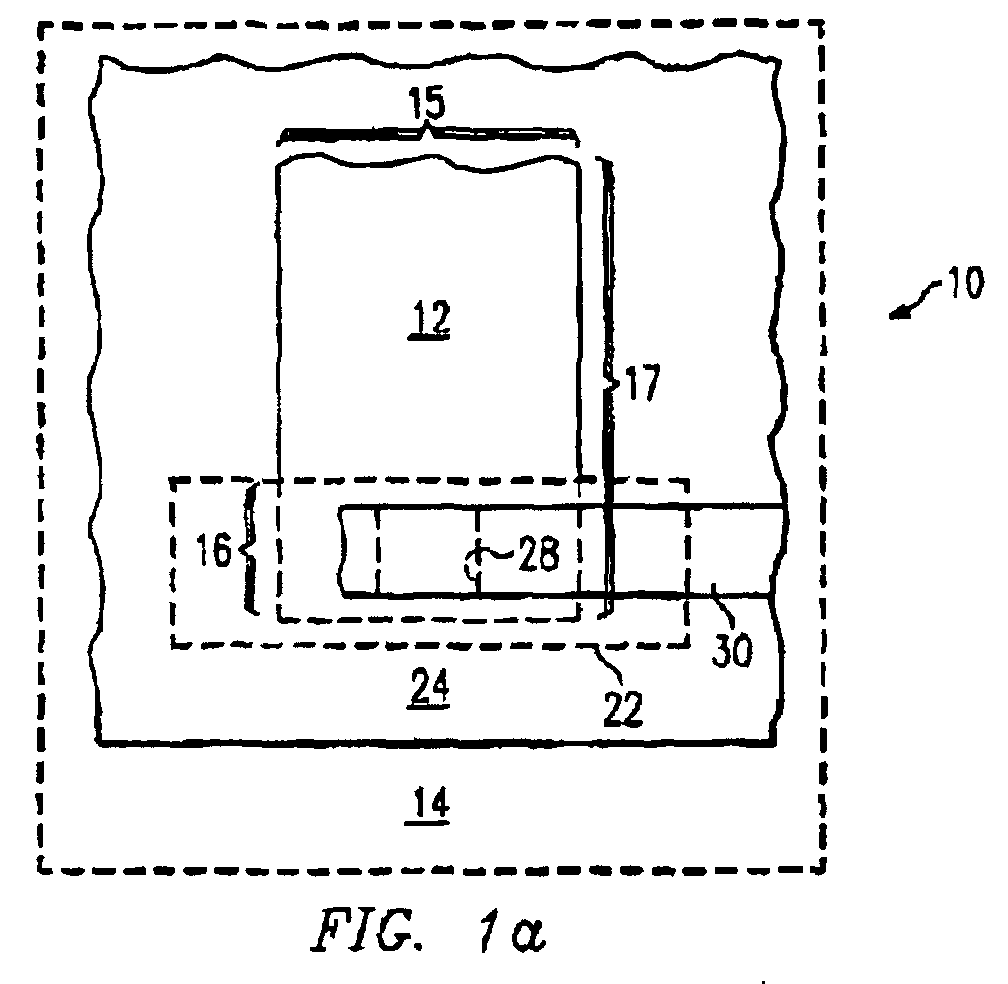
- FIGURES 1A and 1B illustrate top and cross-sectional side views of a portion of an example integrated circuit 10 incorporating a thin film resistor 12 of controlled dimension.
- Integrated circuit 10 may be any suitable type of integrated circuit, for example, a high precision analog integrated circuit.
- Thin film resistor 12 is deposited on a silicon dioxide or other dielectric material 14, below which lies silicon of integrated circuit 10.
- Thin film resistor 12 may include an alloy of nickel and chromium, an alloy of NiCr and aluminum, or any other material suitable for use as a thin film resistor.
- thin film resistor 12 may be approximately 100 ⁇ thick, although the present invention contemplates thin film resistor 12 having any suitable thickness according to particular needs.
- the length and width may be determined to provide a desired resistance of thin film resistor 12 for operation within integrated circuit 10. In particular, it may be desirable to precisely control width 15 of thin film resistor 12.
- the present invention contemplates thin film resistor 12 having any suitable width 15 according to particular needs.
- Thin film resistor 12 includes first and second end portions 16, of which only one is shown.
- a hard mask material 20 may be deposited on and substantially cover a body portion 17 of thin film resistor 12, serving as a hard mask that substantially prevents body portion 17 of thin film resistor 12 from being etched and protects body portion 17 of thin film resistor 12 against diffusion of other materials and contaminates such as planarizing materials into thin film resistor 12.
- hard mask material 20 may include an alloy of titanium and tungsten or any other material suitable for protecting body portion 17 of thin film resistor 12 against seepage of other materials into thin film resistor 12.
- a head mask material 22 such as aluminum, copper, or any other suitable material may cover end portion 16 of thin film resistor 12.
- head mask material 22 is approximately 2500A thick over end portion 16 of thin film resistor 12.
- a dielectric material 24 may cover a portion of head mask material 22 and defme a via 28 formed in dielectric material 24 above an uncovered portion 26 of head mask material 22.
- Dielectric material 24 may include silicon dioxide or any other suitable material.
- a conductive material 30 may be deposited in via 28 and coupled to uncovered portion 26 of head mask material 22 to electrically connect thin film resistor 12 to one or more other components of integrated circuit 10.
- Conductive material 30 may include aluminum, copper, or any other suitable material.
- conductive material 30 and head mask material 22 include substantially similar materials.
- thin film resistor 12 may, in particular embodiments, provide one or more technical advantages. For example, certain embodiments of the present invention may provide the ability to more uniformly and precisely control width 15 of thin film resistor 12 relative to previous techniques. The etch-back or undercutting of thin film resistor 12 associated with wet etching may be significantly reduced or eliminated completely, resulting in decreased width reduction and decreased variation in overall width 15 of thin film resistor 12. In certain embodiments, for example, thin film resistor 12 has a final width of less than approximately 2 ⁇ m and a minimum width 15 reduction that may be scaled down to less than approximately 0.1 ⁇ m, less than approximately 0.05 ⁇ m, less than approximately 0.02 ⁇ m, or better.
- Improved dimension control may allow thin film resistors 12 having more precise resistance to be constructed for precision analog integrated circuits having a reduced minimum width 15 of thin film resistor 12, possibly reducing the overall size of these integrated circuits. Additionally, at least some of these advantages may be achieved in certain embodiments without an additional masking step associated with previous techniques and, instead, with merely non-critical alignment and dimension control patterning steps.
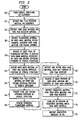
- FIGURE 2 illustrates an example method for constructing thin film resistor 12 of controlled dimension for integrated circuit 10.
- a stencil structure is formed on substrate surface 14, the stencil structure including one or more layers and defining a channel separating first and second opposing portions of the stencil structure.
- the stencil structure may be a lipped stencil structure 80a having a lipped profile.
- Lipped stencil structure 80a may be formed on substrate surface 14 and may include a first stencil structure layer 82, a second stencil structure layer 84, and a channel 86 separating opposing first and second portions 88 of stencil structure 80a, each portion 88 having a lipped profile 90 such that channel 86 is wider at the level of first stencil structure layer 82 than at the level of second stencil structure layer 84.
- first stencil structure layer 82 may include an oxide, phosphorous silicate glass (PSG), undoped silicate glass (USG), or any other suitable material
- second stencil structure layer 84 may include a nitride, USG, or any other suitable material.
- the stencil structure may be an angled stencil structure 80b having an angled profile. Angled stencil structure 80b may be formed on substrate 14 and may include a single layer of a negative resist material 94. A channel 86 separating first and second opposing portions 88 of stencil structure 80b, each portion having an angled profile 92 such that channel 86 is wider at the bottom than at the top.
- FIGURES 3 and 4 illustrate example stencil structures 80 only. Although the remainder of the example method is described with reference to lipped stencil structure 80a, those skilled in the art will appreciate that any suitable stencil structure may be used without departing from the intended scope of the present invention.
- the thin film resistor material is deposited on the surface of substrate 14, with at least some of the thin film resistor material being deposited as desired within channel 86 to define thin film resistor 12. Some of the thin film resistor material may also be deposited outside of channel 86 on first and second opposing portions 88 of stencil structure 80. In one embodiment, the thin film resistor material is deposited using collimated beams directed substantially perpendicular to the surface of substrate 14. At step 54, hard mask material 20 may be deposited on thin film resistor 12 within channel 86 as desired, substantially covering thin film resistor 12.
- hard mask material 20 may also be deposited outside of channel 86 on first and second opposing portions 88 of stencil structure 80, including any thin film resistor material previously deposited on opposing portions 88.
- hard mask material 20 is deposited using collimated beams, which include hard mask material 20 and are directed substantially perpendicular to the surface of substrate 14.
- a planarizing material is deposited on hard mask material 20 within channel 86, the planarizing material substantially filling channel 86 to cover and isolate thin film resistor 12 and hard mask material 20 within channel 86.
- the planarizing material may also substantially cover first and second opposing portions 88 of stencil structure 80, including any thin film resistor material and hard mask material 20 previously deposited on opposing portions 88.
- step 58 at least some of the planarizing material is removed to expose hard mask material 20 deposited outside of channel 86 on first and second opposing portions 88 of stencil structure 80.
- Hard mask material 20 deposited on thin film resistor 12 within channel 86 remains substantially covered by the planarizing material.
- step 60 hard mask material 20 deposited on first and second opposing portions 88 of stencil structure 80 is removed and, at step 62, the thin film resistor material deposited on first and second opposing portions 88 of stencil structure 80 is removed.
- Hard mask material 20 and thin film resistor material deposited on first and second opposing portions 88 of stencil structure 80 may be removed using conventional wet etching techniques, the planarizing material within channel 86 protecting thin film resistor 12 against undesirable etch-back and undercutting and thus from undesirable width reduction.
- first and second opposing portions 88 of stencil structure 80 are removed, leaving thin film resistor 12, hard mask material 20 deposited on thin film resistor 12, and the planarizing material deposited on hard mask material 20 within channel 86 (now resembling an exposed plug) remaining.
- the remaining planarizing material is removed, for example, using conventional techniques.
- head mask material 22 is deposited over end portion 16 of thin film resistor 12, substantially covering end portion 16 of thin film resistor 12 (and thus hard mask material 20 deposited on end portion 16 of thin film resistor 12).
- head mask material 22 is removed, for example, using conventional techniques. In one embodiment, the portion of hard mask material 20 removed is sufficient to expose the entire portion of thin film resister 12 not covered by head mask material 22.
- Dielectric material 24 may be deposited over head mask material 22 and thin film resistor 12 at step 72 and, at step 74, a via 28 may be formed in dielectric material 24 above head mask material 22 to define uncovered portion 26 of head mask material 22.
- conductive material 30 may be deposited in via 28 and coupled to uncovered portion 26 of head mask material 22 to electrically connect thin film resistor 12 to one or more other components of integrated circuit 10, and the method ends.
- FIGURES 5A-5S illustrate an example process for constructing a thin film resistor 12 using a lipped stencil structure 80a.
- a lipped stencil structure 80a angled stencil structure 80b or any other suitable stencil structure may be used according to particular needs.
- first stencil structure layer 82 is deposited on substrate 14 and second stencil structure layer 84 is deposited on first stencil structure layer 82.
- second stencil structure layer 84 is deposited on first stencil structure layer 82.
- a resist 100 is placed on second stencil structure layer 84 and patterned so as to define interior walls 102.
- resist 100 is a positive or negative photoresist patterned using a suitable lithographic masking process.
- channel 86 is formed in first stencil structure layer 82 and second stencil structure layer 84 separating first and second opposing portions 88 of stencil structure 80a.
- Channel 86 may be formed using a dry etching process or any other suitable etching process.
- lipped profile 90 may be formed using an etching process that is selective to the material of first stencil structure layer 82 relative to the material of second stencil structure layer 84, such that first stencil structure layer 82 is etched at a faster rate than second stencil structure layer 84.
- the etching process used to form lipped profile 90 may include exposing stencil structure 80a to a vapor containing hydrofluoric acid (commonly referred to as an "HF" process).
- first stencil structure layer 82 includes a PSG or USG oxide and second stencil structure layer 84 includes a USG oxide or a nitride
- resist 100 is removed from lipped stencil structure 80a using, for example, a lift-off technique such as a standard ashing technique.
- Lipped stencil structure 80a now includes first stencil structure layer 82, second stencil structure layer 84, and channel 86 separating opposing first and second portions 88, each portion 88 including lipped profile 90 such that such that channel 86 is wider at the level of first stencil structure layer 82 than at the level of second stencil structure layer 84.
- the thin film resistor material is deposited on lipped stencil structure 80a, at least some of the thin film resistor material being deposited on the surface of substrate 14 within channel 86 to define thin film resistor 12.
- a portion of the thin film resistor material 104 may also be deposited outside of channel 86 on first and second opposing portions 88 of lipped stencil structure 80a.
- the width of channel 86 at or near the bottom of second stencil structure layer 84 which may be substantially similar to the width of channel 86 at or near the top of second stencil structure layer 84, may determine width 15 of thin film resistor 12 at the bottom of channel 86.
- the width of channel 86 at or near the top of angled stencil structure 80b may determine width 15 of thin film resistor 12 at the bottom of channel 86.
- the thin film resistor material is deposited using collimated beams 106 that include the thin film resistor material and are directed substantially perpendicular to the surface of substrate 14.
- collimated beams 106 directed substantially perpendicular to the surface of substrate 14, combined with lipped profile 90 of lipped stencil structure 80a, may be preferable to increase the probability that width 15 of thin film resistor 12 is substantially similar to the width of channel 86 at or near second stencil structure layer 84 and that thin film resistor 12 is substantially separated from and does not contact first stencil structure layer 82 within channel 86. As described below, this may help ensure that thin film resistor 12 is substantially isolated from first stencil structure layer 82 when channel 86 is filled with the planarizing material, which may in turn substantially reduce or eliminate etch-back or undercutting of thin film resistor 12 during wet etching to remove stencil structure layers 82 and 84.
- hard mask material 20 may be deposited on thin film resistor 12 within channel 86, substantially covering thin film resistor 12. Hard mask material 20 may also be deposited outside of channel 86 on first and second opposing portions 88 of lipped stencil structure 80, including any thin film resistor material 104 previously deposited on opposing portions 88. In one embodiment, hard mask material 20 is deposited using collimated beams 108 that include hard mask material 20 and are directed substantially perpendicular to the surface of substrate 14. The use of collimated beams 108 directed substantially perpendicular to the surface of substrate 14 may be preferable to increase the probability that hard mask material 20 is substantially separated from and does not contact first stencil structure layer 82 within channel 86. Although hard mask material 20 is described, the present invention contemplates formation of thin film resistor 12 without subsequent deposition of hard mask material 20.
- planarizing material 110 is deposited on hard mask material 20 within channel 86, planarizing material 110 substantially filling channel 86 to cover and isolate thin film resistor 12 and hard mask material 20 within channel 86.
- Planarizing material 110 preferably fills the area within channel 86 below stencil structure layer 84 and between first stencil structure layer 82 and thin film resistor 12 so as to substantially separate thin film resistor 12 from first stencil structure layer 82.
- Planarizing material 110 may also substantially cover first and second opposing portions 88 of lipped stencil structure 80a outside of channel 86.
- planarizing material 110 may include polyimide, a photoresist material, a suitable organic material, a plasma oxide, an inorganic dielectric, silicate spin-on glass (SOG) oxide, PC3-1500 manufactured by FUTURREX, INC., or any other suitable material according to particular needs. As shown in FIGURE 51, at least some planarizing material 110 is removed to expose hard mask material 20 deposited outside of channel 86 on first and second opposing portions 88 of lipped stencil structure 80a.
- Planarizing material 110 may be removed using standard ashing techniques, non-critical reverse-block patterning and etch-back, or any other suitable technique according to particular needs. Hard mask material 20 deposited on thin film resistor 12 within channel 86 remains substantially covered by planarizing material 110.
- planarizing material 110 includes an inorganic dielectric such as plasma-enhanced tetra-ethyl-ortho-silicate (TEOS) or silicon dioxide.
- TEOS plasma-enhanced tetra-ethyl-ortho-silicate
- CMP chemical mechanical polishing
- thin film resistor material 104 and hard mask material 20 deposited outside of channel 86 on first and second opposing portions 88 of lipped stencil structure 80a may be removed using standard etching techniques.
- thin film resistor material 104 and hard mask material 20 deposited outside of channel 86 are removed using a standard wet etching technique.
- a CMP technique may be used to remove thin film resistor material 104 and hard mask material 20 deposited outside of channel 86.
- first and second opposing portions 88 of lipped stencil structure 80a may be continued to remove thin film resistor material 104 and hard mask material 20 deposited outside of channel 86.
- the first and second opposing portions 88 of lipped stencil structure 80a, thin film resistor 12, hard mask material 20 deposited on thin film resistor 12, and planarizing material 110 deposited on hard mask material 20 within channel 86 remain.
- Planarizing material 110 deposited on hard mask material 20 within channel 86 may serve as a protective layer for thin film resistor 12 and hard mask material 20 deposited on thin film resistor 12. This may allow a standard wet etching technique to be used to remove thin film resistor material 104 and hard mask material 20 deposited outside of channel 86, and to remove first and second opposing portions 88 of lipped stencil structure 80a themselves, without exposing thin film resistor 12 or hard mask material 20 to wet etching. Thus, the etch-back or undercutting of thin film resistor 12 associated with wet etching may be significantly reduced or eliminated completely, resulting in decreased or eliminated width reduction and variation in overall width 15 of thin film resistor 12 due to such wet etching.
- thin film resistor 12 has a final width of less than approximately 2 ⁇ m and a minimum width reduction that may be scaled down to less than approximately 0.1 ⁇ m, less than approximately 0.05 ⁇ m, less than approximately 0.02 ⁇ m, or better. Improved dimension control may allow thin film resistors 12 having more precise resistance to be constructed, which may decrease yield losses during manufacturing of high precision analog circuits incorporating such thin film resistors 12.
- thin film resistor material 104 and hard mask material 20 deposited outside of channel 86 on first and second opposing portions 88 of lipped stencil structure 80a may be removed using any suitable technique.
- second stencil structure layer 84 may be removed using a plasma strip, dry etch with fluorinated gas, an HF strip, or any other suitable technique.
- first stencil structure layer 82 may be removed using a hydrofluoric acid wet etch or any other suitable technique.
- a CMP technique may be used to remove second stencil structure layer 84. For example, if a CMP technique was used to remove planarizing material 110 to expose hard mask material 20 deposited outside channel 86 on first and second opposing portions 88 of lipped stencil structure 80a and to remove thin film resistor material 104 and hard mask material 20 deposited outside of channel 86, the same CMP technique may be continued to remove second stencil structure layer 84.
- first and second opposing portions 88 may be removed, for example, using a standard ashing technique. As shown in FIGURE 5M, the remaining planarizing material 110 (now resembling an exposed plug) may be removed using a standard ashing technique, solvent strip, or any other suitable technique. Thin film resistor 12 and hard mask material 20 deposited on thin film resistor 12 remain.
- head mask material 22 may be deposited over end portion 16 of thin film resistor 12, substantially covering end portion 16 of thin film resistor 12 (and thus hard mask material 20 deposited on end portion 16 of thin film resistor 12). In one embodiment, approximately 2500A of head mask material 22 are deposited over end portion 16 of thin film resistor 12, although head mask material 22 may have any suitable thickness according to particular needs.
- FIGURE 50 illustrates a top view of a portion of integrated circuit 10 having thin film resistor 12 as formed in FIGURE 5N. In one embodiment, head mask material 22 is deposited over substantially all of integrated circuit 10 and then etched to expose a portion of hard mask material 20 deposited on thin film resistor 12 between ends 16 of thin film resistor 12.
- the exposed portion of hard mask material 20 deposited on thin film resistor 12 may serve as a protective layer for thin film resistor 12 during etching of head mask material 22.
- at least a portion of hard mask material 20 not covered by head mask material 22 is removed, for example, using conventional techniques.
- the portion of hard mask material 20 removed is sufficient to expose the entire portion of thin film resistor 12 not covered by head mask material 22.
- a wet etch, dry etch (e.g., using fluorinated plasma), or other suitable etching technique may be used to remove the portion of hard mask material 20 not covered by head mask material 22.
- dielectric material 24 may be deposited over head mask material 22.
- Dielectric material 24 may include silicon dioxide or any other suitable material.
- a via 28 may be formed in dielectric material 24 above head mask material 22 to define uncovered portion 26 of head mask material 22.
- conductive material 30 may be deposited in via 28 and coupled to uncovered portion 26 of head mask material 22 to electrically connect thin film resistor 12 to one or more other components of integrated circuit 10, and the process ends.
Landscapes
- Semiconductor Integrated Circuits (AREA)
- Apparatuses And Processes For Manufacturing Resistors (AREA)
Abstract
Description
- This invention relates generally to integrated circuits, and more particularly to providing high precision resistance in an integrated circuit using a thin film resistor of controlled dimension.
- Thin film resistors are often used in precision analog-to-digital and digital-to-analog integrated circuits for precision data conversion, which may require precise control of the resistance of the thin film resistor over the operating temperatures. Often the final fine control of the resistance of these precision thin film resistors must be done using laser trimming. For certain integrated circuits, such as high-speed and/or high-frequency precision circuits for example, a low resistivity material may be required to, for example: reduce the resistive-capacitive (RC)-time constant of the integrated circuit; minimize the thickness of the thin film resistor for ease of laser trimming; and reduce the integrated circuit area for low cost. A widely used thin film resistor may be formed, for example, from a deposited layer of nickel and chromium alloy and defined using wet chemical etching to remove unwanted thin film resistor material. Such wet etching techniques are used because currently the thin film resistor material may not be removable using dry etching techniques suitable for large-scale manufacturing of integrated circuits. However, such wet etching techniques may suffer from dimension control problems such as etch-back or undercutting of the thin film resistor body, resulting in undesirable width reduction and variation in overall width of the thin film resistor body. Because the width of the thin film resistor can substantially affect the resistance of the thin film resistor, such dimension control problems may impair the ability to construct thin film resistors having a precise resistance and may result in yield losses during manufacturing of precision integrated analog circuits incorporating such thin film resistors.
- According to the present invention, disadvantages and problems associated with previous techniques for defining thin film resistors for integrated circuits may be reduced or eliminated.
- In one embodiment of the present invention, an integrated circuit includes a thin film resistor, which includes a resistor material that has been deposited on a substrate surface within a channel defined by opposing first and second portions of a stencil structure formed on the substrate surface, the resistor material having an initial width determined by a width of the channel. The stencil structure has been adapted to receive a planarizing material that protects against reduction of the initial width of the resistor material during subsequent process steps for removing the stencil structure. A head mask overlays an end portion of the thin film resistor and a dielectric overlays the head mask, the dielectric defining a via formed in the dielectric above a portion of the head mask. A conductive material has been deposited in the via, coupled to the portion of the head mask and electrically connecting the thin film resistor to other components of the integrated circuit.
- Particular embodiments of the present invention may provide one or more technical advantages. For example, certain embodiments may provide the ability to more uniformly and precisely control the width of the thin film resistor relative to previous techniques. The etch-back or undercutting of the thin film resistor associated with wet etching may be significantly reduced or eliminated completely, resulting in decreased width reduction and decreased variation in the overall width of the thin film resistor. In certain embodiments, for example, the thin film resistor has a final width of less than approximately 2µm and the minimum width reduction of the thin film resistor may be scaled down to less than approximately 0.1µm, less than approximately 0.05µm, less than approximately 0.02µm, or better. Improved dimension control may allow thin film resistors having more precise resistance to be constructed for precision analog integrated circuits having a reduced minimum thin film resistor width, possibly reducing the overall size of these integrated circuits. Additionally, at least some of these advantages may be achieved in certain embodiments without an additional masking step associated with previous techniques and, instead, with merely non-critical alignment and dimension control patterning steps.
- Systems and methods incorporating one or more of these or other technical advantages may be well suited for modem integrated circuit fabrication. Certain embodiments of the present invention may provide all, some, or none of the above advantages. Certain embodiments may provide one or more other technical advantages, one or more of which may be readily apparent to those skilled in the art from the figures, descriptions, and claims included herein.
- For a more complete understanding of the present invention and the advantages thereof, reference is now made to the following descriptions, taken in conjunction with the accompanying drawings in which:
- FIGURES 1A and 1B illustrate top and cross-sectional side views of a portion of an example integrated circuit incorporating a thin film resistor of controlled dimension;
- FIGURE 2 illustrates an example method for constructing a thin film resistor of controlled dimension for an integrated circuit;
- FIGURE 3 illustrates an example stencil structure having a lipped profile;
- FIGURE 4 illustrates an example stencil structure having an angled profile; and
- FIGURES 5A-5S illustrate an example process for constructing a thin film resistor using a stencil structure having a lipped profile.
-
- FIGURES 1A and 1B illustrate top and cross-sectional side views of a portion of an example integrated
circuit 10 incorporating athin film resistor 12 of controlled dimension.Integrated circuit 10 may be any suitable type of integrated circuit, for example, a high precision analog integrated circuit.Thin film resistor 12 is deposited on a silicon dioxide or otherdielectric material 14, below which lies silicon of integratedcircuit 10.Thin film resistor 12 may include an alloy of nickel and chromium, an alloy of NiCr and aluminum, or any other material suitable for use as a thin film resistor. In a particular embodiment,thin film resistor 12 may be approximately 100Å thick, although the present invention contemplatesthin film resistor 12 having any suitable thickness according to particular needs. The length and width may be determined to provide a desired resistance ofthin film resistor 12 for operation within integratedcircuit 10. In particular, it may be desirable to precisely controlwidth 15 ofthin film resistor 12. The present invention contemplatesthin film resistor 12 having anysuitable width 15 according to particular needs. -
Thin film resistor 12 includes first andsecond end portions 16, of which only one is shown. Ahard mask material 20 may be deposited on and substantially cover abody portion 17 ofthin film resistor 12, serving as a hard mask that substantially preventsbody portion 17 ofthin film resistor 12 from being etched and protectsbody portion 17 ofthin film resistor 12 against diffusion of other materials and contaminates such as planarizing materials intothin film resistor 12. Afterbody portion 17 ofthin film resistor 12, which is covered withhard mask material 20, has been formed according to the methods of the present invention,hard mask material 20 may include an alloy of titanium and tungsten or any other material suitable for protectingbody portion 17 ofthin film resistor 12 against seepage of other materials intothin film resistor 12. Ahead mask material 22 such as aluminum, copper, or any other suitable material may coverend portion 16 ofthin film resistor 12. In one embodiment,head mask material 22 is approximately 2500A thick overend portion 16 ofthin film resistor 12. Adielectric material 24 may cover a portion ofhead mask material 22 and defme avia 28 formed indielectric material 24 above anuncovered portion 26 ofhead mask material 22.Dielectric material 24 may include silicon dioxide or any other suitable material. Aconductive material 30 may be deposited in via 28 and coupled to uncoveredportion 26 ofhead mask material 22 to electrically connectthin film resistor 12 to one or more other components of integratedcircuit 10.Conductive material 30 may include aluminum, copper, or any other suitable material. In one embodiment,conductive material 30 andhead mask material 22 include substantially similar materials. - Formation of
thin film resistor 12 according to the present invention may, in particular embodiments, provide one or more technical advantages. For example, certain embodiments of the present invention may provide the ability to more uniformly and precisely controlwidth 15 ofthin film resistor 12 relative to previous techniques. The etch-back or undercutting ofthin film resistor 12 associated with wet etching may be significantly reduced or eliminated completely, resulting in decreased width reduction and decreased variation inoverall width 15 ofthin film resistor 12. In certain embodiments, for example,thin film resistor 12 has a final width of less than approximately 2µm and aminimum width 15 reduction that may be scaled down to less than approximately 0.1µm, less than approximately 0.05µm, less than approximately 0.02µm, or better. Improved dimension control may allowthin film resistors 12 having more precise resistance to be constructed for precision analog integrated circuits having a reducedminimum width 15 ofthin film resistor 12, possibly reducing the overall size of these integrated circuits. Additionally, at least some of these advantages may be achieved in certain embodiments without an additional masking step associated with previous techniques and, instead, with merely non-critical alignment and dimension control patterning steps. - FIGURE 2 illustrates an example method for constructing
thin film resistor 12 of controlled dimension for integratedcircuit 10. Atstep 50, a stencil structure is formed onsubstrate surface 14, the stencil structure including one or more layers and defining a channel separating first and second opposing portions of the stencil structure. - For example, referring to FIGURE 3, the stencil structure may be a lipped
stencil structure 80a having a lipped profile.Lipped stencil structure 80a may be formed onsubstrate surface 14 and may include a firststencil structure layer 82, a secondstencil structure layer 84, and achannel 86 separating opposing first andsecond portions 88 ofstencil structure 80a, eachportion 88 having a lippedprofile 90 such thatchannel 86 is wider at the level of firststencil structure layer 82 than at the level of secondstencil structure layer 84. In one embodiment, firststencil structure layer 82 may include an oxide, phosphorous silicate glass (PSG), undoped silicate glass (USG), or any other suitable material, and secondstencil structure layer 84 may include a nitride, USG, or any other suitable material. As another example, referring to FIGURE 4, the stencil structure may be anangled stencil structure 80b having an angled profile.Angled stencil structure 80b may be formed onsubstrate 14 and may include a single layer of anegative resist material 94. Achannel 86 separating first and secondopposing portions 88 ofstencil structure 80b, each portion having anangled profile 92 such thatchannel 86 is wider at the bottom than at the top. FIGURES 3 and 4 illustrate example stencil structures 80 only. Although the remainder of the example method is described with reference tolipped stencil structure 80a, those skilled in the art will appreciate that any suitable stencil structure may be used without departing from the intended scope of the present invention. - Returning to FIGURE 2, at
step 52, the thin film resistor material is deposited on the surface ofsubstrate 14, with at least some of the thin film resistor material being deposited as desired withinchannel 86 to definethin film resistor 12. Some of the thin film resistor material may also be deposited outside ofchannel 86 on first and second opposingportions 88 of stencil structure 80. In one embodiment, the thin film resistor material is deposited using collimated beams directed substantially perpendicular to the surface ofsubstrate 14. Atstep 54,hard mask material 20 may be deposited onthin film resistor 12 withinchannel 86 as desired, substantially coveringthin film resistor 12. Somehard mask material 20 may also be deposited outside ofchannel 86 on first and second opposingportions 88 of stencil structure 80, including any thin film resistor material previously deposited on opposingportions 88. In one embodiment,hard mask material 20 is deposited using collimated beams, which includehard mask material 20 and are directed substantially perpendicular to the surface ofsubstrate 14. At step 56, a planarizing material is deposited onhard mask material 20 withinchannel 86, the planarizing material substantially fillingchannel 86 to cover and isolatethin film resistor 12 andhard mask material 20 withinchannel 86. The planarizing material may also substantially cover first and second opposingportions 88 of stencil structure 80, including any thin film resistor material andhard mask material 20 previously deposited on opposingportions 88. - At
step 58, at least some of the planarizing material is removed to exposehard mask material 20 deposited outside ofchannel 86 on first and second opposingportions 88 of stencil structure 80.Hard mask material 20 deposited onthin film resistor 12 withinchannel 86 remains substantially covered by the planarizing material. Atstep 60,hard mask material 20 deposited on first and second opposingportions 88 of stencil structure 80 is removed and, atstep 62, the thin film resistor material deposited on first and second opposingportions 88 of stencil structure 80 is removed.Hard mask material 20 and thin film resistor material deposited on first and second opposingportions 88 of stencil structure 80 may be removed using conventional wet etching techniques, the planarizing material withinchannel 86 protectingthin film resistor 12 against undesirable etch-back and undercutting and thus from undesirable width reduction. Atstep 64, first and second opposingportions 88 of stencil structure 80 are removed, leavingthin film resistor 12,hard mask material 20 deposited onthin film resistor 12, and the planarizing material deposited onhard mask material 20 within channel 86 (now resembling an exposed plug) remaining. Atstep 66, the remaining planarizing material is removed, for example, using conventional techniques. - At
step 68,head mask material 22 is deposited overend portion 16 ofthin film resistor 12, substantially coveringend portion 16 of thin film resistor 12 (and thushard mask material 20 deposited onend portion 16 of thin film resistor 12). Atstep 70, at least a portion ofhard mask material 20 not covered byhead mask material 22 is removed, for example, using conventional techniques. In one embodiment, the portion ofhard mask material 20 removed is sufficient to expose the entire portion ofthin film resister 12 not covered byhead mask material 22.Dielectric material 24 may be deposited overhead mask material 22 andthin film resistor 12 atstep 72 and, atstep 74, a via 28 may be formed indielectric material 24 abovehead mask material 22 to define uncoveredportion 26 ofhead mask material 22. Atstep 76,conductive material 30 may be deposited in via 28 and coupled to uncoveredportion 26 ofhead mask material 22 to electrically connectthin film resistor 12 to one or more other components ofintegrated circuit 10, and the method ends. - FIGURES 5A-5S illustrate an example process for constructing a
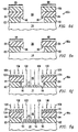
thin film resistor 12 using alipped stencil structure 80a. Although the illustrated example involves alipped stencil structure 80a,angled stencil structure 80b or any other suitable stencil structure may be used according to particular needs. As shown in FIGURE 5A, to formlipped stencil structure 80a, firststencil structure layer 82 is deposited onsubstrate 14 and secondstencil structure layer 84 is deposited on firststencil structure layer 82. As shown in FIGURE 5B, a resist 100 is placed on secondstencil structure layer 84 and patterned so as to defineinterior walls 102. In one embodiment, resist 100 is a positive or negative photoresist patterned using a suitable lithographic masking process. - As shown in FIGURE 5C,
channel 86 is formed in firststencil structure layer 82 and secondstencil structure layer 84 separating first and second opposingportions 88 ofstencil structure 80a.Channel 86 may be formed using a dry etching process or any other suitable etching process. As shown in FIGURE 5D,lipped profile 90 may be formed using an etching process that is selective to the material of firststencil structure layer 82 relative to the material of secondstencil structure layer 84, such that firststencil structure layer 82 is etched at a faster rate than secondstencil structure layer 84. The etching process used to formlipped profile 90 may include exposingstencil structure 80a to a vapor containing hydrofluoric acid (commonly referred to as an "HF" process). As an example, if firststencil structure layer 82 includes a PSG or USG oxide and secondstencil structure layer 84 includes a USG oxide or a nitride, it may be preferable to exposelipped stencil structure 80a to a dilute hydrofluoric vapor or acid to formlipped profile 90. As shown in FIGURE 5E, resist 100 is removed fromlipped stencil structure 80a using, for example, a lift-off technique such as a standard ashing technique.Lipped stencil structure 80a now includes firststencil structure layer 82, secondstencil structure layer 84, andchannel 86 separating opposing first andsecond portions 88, eachportion 88 includinglipped profile 90 such that such thatchannel 86 is wider at the level of firststencil structure layer 82 than at the level of secondstencil structure layer 84. - As shown in FIGURE 5F, the thin film resistor material is deposited on
lipped stencil structure 80a, at least some of the thin film resistor material being deposited on the surface ofsubstrate 14 withinchannel 86 to definethin film resistor 12. A portion of the thinfilm resistor material 104 may also be deposited outside ofchannel 86 on first and second opposingportions 88 oflipped stencil structure 80a. The width ofchannel 86 at or near the bottom of secondstencil structure layer 84, which may be substantially similar to the width ofchannel 86 at or near the top of secondstencil structure layer 84, may determinewidth 15 ofthin film resistor 12 at the bottom ofchannel 86. Similarly, in an alternative embodiment in which angledstencil structure 80b is used, the width ofchannel 86 at or near the top ofangled stencil structure 80b may determinewidth 15 ofthin film resistor 12 at the bottom ofchannel 86. In one embodiment, the thin film resistor material is deposited using collimatedbeams 106 that include the thin film resistor material and are directed substantially perpendicular to the surface ofsubstrate 14. The use of collimatedbeams 106 directed substantially perpendicular to the surface ofsubstrate 14, combined withlipped profile 90 oflipped stencil structure 80a, may be preferable to increase the probability thatwidth 15 ofthin film resistor 12 is substantially similar to the width ofchannel 86 at or near secondstencil structure layer 84 and thatthin film resistor 12 is substantially separated from and does not contact firststencil structure layer 82 withinchannel 86. As described below, this may help ensure thatthin film resistor 12 is substantially isolated from firststencil structure layer 82 whenchannel 86 is filled with the planarizing material, which may in turn substantially reduce or eliminate etch-back or undercutting ofthin film resistor 12 during wet etching to remove stencil structure layers 82 and 84. - As shown in FIGURE 5G,
hard mask material 20 may be deposited onthin film resistor 12 withinchannel 86, substantially coveringthin film resistor 12.Hard mask material 20 may also be deposited outside ofchannel 86 on first and second opposingportions 88 of lipped stencil structure 80, including any thinfilm resistor material 104 previously deposited on opposingportions 88. In one embodiment,hard mask material 20 is deposited using collimatedbeams 108 that includehard mask material 20 and are directed substantially perpendicular to the surface ofsubstrate 14. The use of collimatedbeams 108 directed substantially perpendicular to the surface ofsubstrate 14 may be preferable to increase the probability thathard mask material 20 is substantially separated from and does not contact firststencil structure layer 82 withinchannel 86. Althoughhard mask material 20 is described, the present invention contemplates formation ofthin film resistor 12 without subsequent deposition ofhard mask material 20. - As shown in FIGURE 5H,
planarizing material 110 is deposited onhard mask material 20 withinchannel 86,planarizing material 110 substantially fillingchannel 86 to cover and isolatethin film resistor 12 andhard mask material 20 withinchannel 86.Planarizing material 110 preferably fills the area withinchannel 86 belowstencil structure layer 84 and between firststencil structure layer 82 andthin film resistor 12 so as to substantially separatethin film resistor 12 from firststencil structure layer 82.Planarizing material 110 may also substantially cover first and second opposingportions 88 oflipped stencil structure 80a outside ofchannel 86. It may be preferable to minimize formation of a significant recess in the top surface ofplanarizing material 110 overchannel 86, such thatplanarizing material 110 preferably completely fillschannel 86 and the top surface ofplanarizing material 110 is substantially level.Planarizing material 110 may include polyimide, a photoresist material, a suitable organic material, a plasma oxide, an inorganic dielectric, silicate spin-on glass (SOG) oxide, PC3-1500 manufactured by FUTURREX, INC., or any other suitable material according to particular needs. As shown in FIGURE 51, at least someplanarizing material 110 is removed to exposehard mask material 20 deposited outside ofchannel 86 on first and second opposingportions 88 oflipped stencil structure 80a.Planarizing material 110 may be removed using standard ashing techniques, non-critical reverse-block patterning and etch-back, or any other suitable technique according to particular needs.Hard mask material 20 deposited onthin film resistor 12 withinchannel 86 remains substantially covered byplanarizing material 110. In certain embodiments,planarizing material 110 includes an inorganic dielectric such as plasma-enhanced tetra-ethyl-ortho-silicate (TEOS) or silicon dioxide. In this embodiment, a chemical mechanical polishing (CMP) technique may be used to removeplanarizing material 110 to exposehard mask material 20 deposited outside ofchannel 86 on first and second opposingportions 88 oflipped stencil structure 80a. - As shown in FIGURE 5J, thin
film resistor material 104 andhard mask material 20 deposited outside ofchannel 86 on first and second opposingportions 88 oflipped stencil structure 80a may be removed using standard etching techniques. In one embodiment, thinfilm resistor material 104 andhard mask material 20 deposited outside ofchannel 86 are removed using a standard wet etching technique. In an alternative embodiment, a CMP technique may be used to remove thinfilm resistor material 104 andhard mask material 20 deposited outside ofchannel 86. For example, if a CMP technique was used to removeplanarizing material 110 to exposehard mask material 20 deposited outsidechannel 86 on first and second opposingportions 88 oflipped stencil structure 80a, the same CMP technique may be continued to remove thinfilm resistor material 104 andhard mask material 20 deposited outside ofchannel 86. The first and second opposingportions 88 oflipped stencil structure 80a,thin film resistor 12,hard mask material 20 deposited onthin film resistor 12, andplanarizing material 110 deposited onhard mask material 20 withinchannel 86 remain. -
Planarizing material 110 deposited onhard mask material 20 withinchannel 86 may serve as a protective layer forthin film resistor 12 andhard mask material 20 deposited onthin film resistor 12. This may allow a standard wet etching technique to be used to remove thinfilm resistor material 104 andhard mask material 20 deposited outside ofchannel 86, and to remove first and second opposingportions 88 oflipped stencil structure 80a themselves, without exposingthin film resistor 12 orhard mask material 20 to wet etching. Thus, the etch-back or undercutting ofthin film resistor 12 associated with wet etching may be significantly reduced or eliminated completely, resulting in decreased or eliminated width reduction and variation inoverall width 15 ofthin film resistor 12 due to such wet etching. In certain embodiments, for example,thin film resistor 12 has a final width of less than approximately 2µm and a minimum width reduction that may be scaled down to less than approximately 0.1µm, less than approximately 0.05µm, less than approximately 0.02µm, or better. Improved dimension control may allowthin film resistors 12 having more precise resistance to be constructed, which may decrease yield losses during manufacturing of high precision analog circuits incorporating suchthin film resistors 12. Although wet etching is described, thinfilm resistor material 104 andhard mask material 20 deposited outside ofchannel 86 on first and second opposingportions 88 oflipped stencil structure 80a may be removed using any suitable technique. - As shown in FIGURE 5K, second
stencil structure layer 84 may be removed using a plasma strip, dry etch with fluorinated gas, an HF strip, or any other suitable technique. As shown in FIGURE 5L, firststencil structure layer 82 may be removed using a hydrofluoric acid wet etch or any other suitable technique. In one embodiment, a CMP technique may be used to remove secondstencil structure layer 84. For example, if a CMP technique was used to removeplanarizing material 110 to exposehard mask material 20 deposited outsidechannel 86 on first and second opposingportions 88 oflipped stencil structure 80a and to remove thinfilm resistor material 104 andhard mask material 20 deposited outside ofchannel 86, the same CMP technique may be continued to remove secondstencil structure layer 84. In an alternative embodiment, ifangled stencil structure 80b is used, first and second opposingportions 88 may be removed, for example, using a standard ashing technique. As shown in FIGURE 5M, the remaining planarizing material 110 (now resembling an exposed plug) may be removed using a standard ashing technique, solvent strip, or any other suitable technique.Thin film resistor 12 andhard mask material 20 deposited onthin film resistor 12 remain. - As shown in FIGURE 5N,
head mask material 22 may be deposited overend portion 16 ofthin film resistor 12, substantially coveringend portion 16 of thin film resistor 12 (and thushard mask material 20 deposited onend portion 16 of thin film resistor 12). In one embodiment, approximately 2500A ofhead mask material 22 are deposited overend portion 16 ofthin film resistor 12, althoughhead mask material 22 may have any suitable thickness according to particular needs. FIGURE 50 illustrates a top view of a portion ofintegrated circuit 10 havingthin film resistor 12 as formed in FIGURE 5N. In one embodiment,head mask material 22 is deposited over substantially all ofintegrated circuit 10 and then etched to expose a portion ofhard mask material 20 deposited onthin film resistor 12 between ends 16 ofthin film resistor 12. The exposed portion ofhard mask material 20 deposited onthin film resistor 12 may serve as a protective layer forthin film resistor 12 during etching ofhead mask material 22. As shown in FIGURE 5P, at least a portion ofhard mask material 20 not covered byhead mask material 22 is removed, for example, using conventional techniques. In one embodiment, the portion ofhard mask material 20 removed is sufficient to expose the entire portion ofthin film resistor 12 not covered byhead mask material 22. A wet etch, dry etch (e.g., using fluorinated plasma), or other suitable etching technique may be used to remove the portion ofhard mask material 20 not covered byhead mask material 22. - As shown in FIGURE 5Q,
dielectric material 24 may be deposited overhead mask material 22.Dielectric material 24 may include silicon dioxide or any other suitable material. As shown in FIGURE 5R, a via 28 may be formed indielectric material 24 abovehead mask material 22 to define uncoveredportion 26 ofhead mask material 22. As shown in FIGURE 5S,conductive material 30 may be deposited in via 28 and coupled to uncoveredportion 26 ofhead mask material 22 to electrically connectthin film resistor 12 to one or more other components ofintegrated circuit 10, and the process ends. - Although the present invention has been described with several embodiments, diverse changes, substitutions, variations, alterations, and modifications may be suggested to one skilled in the art, and it is intended that the invention encompass all such changes, substitutions, variations, alterations, and modifications as fall within the scope of the appended claims.
Claims (10)
- An integrated circuit, comprising:a thin film resistor comprising a thin film resistor material that has been deposited on a substrate surface within a channel defined by opposing first and second portions of a stencil structure formed on the substrate surface, the thin film resistor material having an initial width determined by a width of the channel, the stencil structure having been adapted to receive a planarizing material so as to substantially surround the thin film resistor material within the channel and protect against reduction of the initial width of the thin film resistor material during subsequent process steps for removing the stencil structure from the substrate surface;a head mask material overlaying an end portion of the thin film resistor;a dielectric material overlaying the head mask material and defining a via formed in the dielectric material above a portion of the head mask material; anda conductive material deposited in the via and coupled to the portion of the head mask material, the conductive material electrically connecting the thin film resistor to one or more other components of the integrated circuit.
- The integrated circuit of Claim 1, wherein the integrated circuit comprises a high precision analog integrated circuit.
- A method for constructing a thin film resistor for an integrated circuit, comprising:forming a stencil structure on a substrate surface, the stencil structure comprising one or more layers and defining a channel separating first and second opposing portions of the stencil structure;depositing a thin film resistor material, some of the thin film resistor material being deposited on the substrate surface within the channel to define the thin film resistor, some of the thin film resistor material being deposited outside the channel on the first and second opposing portions of the stencil structure, the thin film resistor having an initial width determined by a width of the channel;depositing a planarizing material within the channel so as to substantially surround the thin film resistor within the channel and protect against reduction of the initial width of the thin film resistor during subsequent process steps for removing the stencil structure from the substrate surface;removing at least some of the planarizing material sufficient to expose the thin film resistor material deposited outside the channel on the first and second opposing portions of the stencil structure, the thin film resistor within the channel remaining covered by the planarizing material;removing the thin film resistor material deposited outside the channel on the first and second opposing portions of the stencil structure;removing the first and second opposing portions of the stencil structure; andremoving the remaining planarizing material deposited on the thin film resistor within the channel.
- The method of Claim 3, wherein the thin film resistor has a final width of less than approximately 2µm.
- The method of Claim 3, wherein the thin film resistor has a final width that differs from the initial width of the thin film resistor by less than approximately 0.1 µm.
- The method of any one of Claims 3 to 5, wherein forming the stencil structure on the substrate surface further comprises:depositing a first stencil structure layer on the substrate surface; anddepositing a second stencil structure layer on the first stencil structure layer, the second stencil structure layer comprising a different material than the first stencil structure layer, the second stencil structure layer extending further into the channel than the first stencil structure layer due to preferential etching of the first stencil structure layer relative to the second stencil structure layer, the width of the channel between opposing second stencil structure layers determining the initial width of the thin film resistor.
- The method of any one of Claims 3 to 6, further comprising:depositing a head mask material overlaying an end portion of the thin film resistor;depositing a dielectric material overlaying the head mask material and defming a via formed in the dielectric material above a portion of the head mask material; anddepositing a conductive material in the via and coupled to the portion of the head mask material, the conductive material electrically connecting the thin film resistor to one or more other components of the integrated circuit.
- The method of Claim 7, further comprising:depositing a hard mask material on substantially all of the thin film resistor within the channel to protect against diffusion of the head mask material into the thin film resistor during operation of the integrated circuit; andremoving a portion of the hard mask material such that the hard mask material covers the end portion of the thin film resistor underlying the head mask material.
- The method of Claim 8, wherein:the thin film resistor material is deposited using first collimated beams comprising the thin film resistor material and directed substantially perpendicular to the substrate surface; andthe hard mask material is deposited using second collimated beams comprising the barrier material and directed substantially perpendicular to the substrate surface.
- The method of Claim 8 or 9, wherein:the thin film resistor material comprises an alloy of nickel and chromium;the hard mask material comprises an alloy of titanium and tungsten;the planarizing material comprises at least one of polyimide, a photoresist material, an organic material, a plasma oxide, and an inorganic dielectric; andthe head mask material and the conductive material comprise at least one of aluminum and copper.
Applications Claiming Priority (2)
| Application Number | Priority Date | Filing Date | Title |
|---|---|---|---|
| US10/271,495 US20040070048A1 (en) | 2002-10-15 | 2002-10-15 | Providing high precision resistance in an integrated circuit using a thin film resistor of controlled dimension |
| US271495 | 2002-10-15 |
Publications (2)
| Publication Number | Publication Date |
|---|---|
| EP1411548A2 true EP1411548A2 (en) | 2004-04-21 |
| EP1411548A3 EP1411548A3 (en) | 2004-06-30 |
Family
ID=32042914
Family Applications (1)
| Application Number | Title | Priority Date | Filing Date |
|---|---|---|---|
| EP03103821A Withdrawn EP1411548A3 (en) | 2002-10-15 | 2003-10-15 | Providing high precision resistance in an integrated circuit using a thin film resistor of controlled dimension |
Country Status (2)
| Country | Link |
|---|---|
| US (2) | US20040070048A1 (en) |
| EP (1) | EP1411548A3 (en) |
Families Citing this family (4)
| Publication number | Priority date | Publication date | Assignee | Title |
|---|---|---|---|---|
| US7112286B2 (en) * | 2003-12-04 | 2006-09-26 | Texas Instruments Incorporated | Thin film resistor structure and method of fabricating a thin film resistor structure |
| US6989327B2 (en) * | 2004-01-31 | 2006-01-24 | Hewlett-Packard Development Company, L.P. | Forming a contact in a thin-film device |
| US8013394B2 (en) * | 2007-03-28 | 2011-09-06 | International Business Machines Corporation | Integrated circuit having resistor between BEOL interconnect and FEOL structure and related method |
| US7733212B2 (en) | 2007-04-26 | 2010-06-08 | Hewlett-Packard Development Company, L.P. | Resistor |
Citations (5)
| Publication number | Priority date | Publication date | Assignee | Title |
|---|---|---|---|---|
| US4256816A (en) * | 1977-10-13 | 1981-03-17 | Bell Telephone Laboratories, Incorporated | Mask structure for depositing patterned thin films |
| EP0230615A2 (en) * | 1986-01-31 | 1987-08-05 | International Business Machines Corporation | Silicon-containing polyimides as oxygen etch stop and dual dielectric coatings |
| US5258264A (en) * | 1989-07-06 | 1993-11-02 | International Business Machines Corporation | Process of forming a dual overhang collimated lift-off stencil with subsequent metal deposition |
| US5670820A (en) | 1987-05-01 | 1997-09-23 | Inmos Limited | Semiconductor element incorporating a resistive device |
| US6400252B1 (en) | 1998-11-13 | 2002-06-04 | Telefonaktiebolaget Lm Ericsson | Polysilicon resistor and a method of producing it |
Family Cites Families (12)
| Publication number | Priority date | Publication date | Assignee | Title |
|---|---|---|---|---|
| US4584761A (en) * | 1984-05-15 | 1986-04-29 | Digital Equipment Corporation | Integrated circuit chip processing techniques and integrated chip produced thereby |
| US4767721A (en) * | 1986-02-10 | 1988-08-30 | Hughes Aircraft Company | Double layer photoresist process for well self-align and ion implantation masking |
| US5420063A (en) * | 1994-04-11 | 1995-05-30 | National Semiconductor Corporation | Method of producing a resistor in an integrated circuit |
| US5547896A (en) * | 1995-02-13 | 1996-08-20 | Harris Corporation | Direct etch for thin film resistor using a hard mask |
| JP3678814B2 (en) * | 1995-09-29 | 2005-08-03 | 日本バーブラウン株式会社 | Integrated circuit resistor array |
| US6165862A (en) * | 1997-08-29 | 2000-12-26 | Denso Corporation | Method of producing a thin film resistor |
| US6441447B1 (en) * | 1998-02-12 | 2002-08-27 | Intersil Corporation | Co-patterning thin-film resistors of different compositions with a conductive hard mask and method for same |
| US6228735B1 (en) * | 1998-12-15 | 2001-05-08 | United Microelectronics Corp. | Method of fabricating thin-film transistor |
| AU6211000A (en) | 1999-07-14 | 2001-02-05 | Lucent Technologies Inc. | A thin film resistor device and a method of manufacture therefor |
| JP3627617B2 (en) * | 2000-04-06 | 2005-03-09 | 株式会社デンソー | Method for processing refractory metal and method for manufacturing semiconductor device using this metal |
| US6426268B1 (en) * | 2000-11-28 | 2002-07-30 | Analog Devices, Inc. | Thin film resistor fabrication method |
| US6607962B2 (en) * | 2001-08-09 | 2003-08-19 | Maxim Integrated Products, Inc. | Globally planarized backend compatible thin film resistor contact/interconnect process |
-
2002
- 2002-10-15 US US10/271,495 patent/US20040070048A1/en not_active Abandoned
-
2003
- 2003-10-15 EP EP03103821A patent/EP1411548A3/en not_active Withdrawn
-
2004
- 2004-06-24 US US10/875,846 patent/US7005361B2/en not_active Expired - Lifetime
Patent Citations (5)
| Publication number | Priority date | Publication date | Assignee | Title |
|---|---|---|---|---|
| US4256816A (en) * | 1977-10-13 | 1981-03-17 | Bell Telephone Laboratories, Incorporated | Mask structure for depositing patterned thin films |
| EP0230615A2 (en) * | 1986-01-31 | 1987-08-05 | International Business Machines Corporation | Silicon-containing polyimides as oxygen etch stop and dual dielectric coatings |
| US5670820A (en) | 1987-05-01 | 1997-09-23 | Inmos Limited | Semiconductor element incorporating a resistive device |
| US5258264A (en) * | 1989-07-06 | 1993-11-02 | International Business Machines Corporation | Process of forming a dual overhang collimated lift-off stencil with subsequent metal deposition |
| US6400252B1 (en) | 1998-11-13 | 2002-06-04 | Telefonaktiebolaget Lm Ericsson | Polysilicon resistor and a method of producing it |
Also Published As
| Publication number | Publication date |
|---|---|
| EP1411548A3 (en) | 2004-06-30 |
| US20040070048A1 (en) | 2004-04-15 |
| US7005361B2 (en) | 2006-02-28 |
| US20040227614A1 (en) | 2004-11-18 |
Similar Documents
| Publication | Publication Date | Title |
|---|---|---|
| US7232736B2 (en) | Semiconductor devices with capacitors of metal/insulator/metal structure and methods for forming the same | |
| US7960240B1 (en) | System and method for providing a dual via architecture for thin film resistors | |
| US6232647B1 (en) | Air gap with borderless contact | |
| US5534462A (en) | Method for forming a plug and semiconductor device having the same | |
| KR100204691B1 (en) | Process for forming a self aligned contact structure | |
| US7323751B2 (en) | Thin film resistor integration in a dual damascene structure | |
| EP1235264A2 (en) | Direct etch for thin film resistor using a hard mask | |
| US8012844B2 (en) | Method of manufacturing an integrated circuit | |
| US7808048B1 (en) | System and method for providing a buried thin film resistor having end caps defined by a dielectric mask | |
| EP1463067B1 (en) | Method of forming an integrated circuit thin film resistor | |
| US20010021581A1 (en) | Patterning conductive lines in circuit structures | |
| EP0326293A1 (en) | Method for forming interconnects | |
| US20010046784A1 (en) | Method of manufacturing a semiconductor device | |
| JP4317015B2 (en) | Metal-to-metal antifuses using carbon-containing antifuse materials | |
| US6497824B1 (en) | One mask solution for the integration of the thin film resistor | |
| US5854503A (en) | Maximization of low dielectric constant material between interconnect traces of a semiconductor circuit | |
| US6117760A (en) | Method of making a high density interconnect formation | |
| US7112286B2 (en) | Thin film resistor structure and method of fabricating a thin film resistor structure | |
| US20010049199A1 (en) | Method of integrating a thin film resistor in a multi-level metal tungsten-plug interconnect | |
| US6218287B1 (en) | Method of fabricating a semiconductor structure | |
| US7005361B2 (en) | Providing high precision resistance in an integrated circuit using a thin film resistor of controlled dimension | |
| US5922515A (en) | Approaches to integrate the deep contact module | |
| US20030030107A1 (en) | Globally planarized backend compatible thin film resistor contact/interconnect process | |
| EP0981161A2 (en) | Semiconductor structure including a conductive fuse and process for fabrication thereof | |
| US8679932B1 (en) | System and method for manufacturing thin film resistors using a trench and chemical mechanical polishing |
Legal Events
| Date | Code | Title | Description |
|---|---|---|---|
| PUAI | Public reference made under article 153(3) epc to a published international application that has entered the european phase |
Free format text: ORIGINAL CODE: 0009012 |
|
| AK | Designated contracting states |
Kind code of ref document: A2 Designated state(s): AT BE BG CH CY CZ DE DK EE ES FI FR GB GR HU IE IT LI LU MC NL PT RO SE SI SK TR |
|
| AX | Request for extension of the european patent |
Extension state: AL LT LV MK |
|
| PUAL | Search report despatched |
Free format text: ORIGINAL CODE: 0009013 |
|
| AK | Designated contracting states |
Kind code of ref document: A3 Designated state(s): AT BE BG CH CY CZ DE DK EE ES FI FR GB GR HU IE IT LI LU MC NL PT RO SE SI SK TR |
|
| AX | Request for extension of the european patent |
Extension state: AL LT LV MK |
|
| RIC1 | Information provided on ipc code assigned before grant |
Ipc: 7H 01L 21/033 B Ipc: 7H 01L 21/02 B Ipc: 7H 01L 27/01 B Ipc: 7H 01L 21/70 A |
|
| 17P | Request for examination filed |
Effective date: 20041230 |
|
| 17Q | First examination report despatched |
Effective date: 20050207 |
|
| AKX | Designation fees paid |
Designated state(s): DE FR GB |
|
| APBK | Appeal reference recorded |
Free format text: ORIGINAL CODE: EPIDOSNREFNE |
|
| APBN | Date of receipt of notice of appeal recorded |
Free format text: ORIGINAL CODE: EPIDOSNNOA2E |
|
| APBR | Date of receipt of statement of grounds of appeal recorded |
Free format text: ORIGINAL CODE: EPIDOSNNOA3E |
|
| APAF | Appeal reference modified |
Free format text: ORIGINAL CODE: EPIDOSCREFNE |
|
| APBX | Invitation to file observations in appeal sent |
Free format text: ORIGINAL CODE: EPIDOSNOBA2E |
|
| APBZ | Receipt of observations in appeal recorded |
Free format text: ORIGINAL CODE: EPIDOSNOBA4E |
|
| APAQ | Information on invitation to file observation in appeal modified |
Free format text: ORIGINAL CODE: EPIDOSCOBA2E |
|
| APBH | Information on receipt of observation in appeal deleted |
Free format text: ORIGINAL CODE: EPIDOSDOBA4E |
|
| APBT | Appeal procedure closed |
Free format text: ORIGINAL CODE: EPIDOSNNOA9E |
|
| STAA | Information on the status of an ep patent application or granted ep patent |
Free format text: STATUS: THE APPLICATION IS DEEMED TO BE WITHDRAWN |
|
| 18D | Application deemed to be withdrawn |
Effective date: 20190612 |