EP1411155A1 - 3c-sic nanowhisker synthesizing method and 3c-sic nanowhisker - Google Patents
3c-sic nanowhisker synthesizing method and 3c-sic nanowhisker Download PDFInfo
- Publication number
- EP1411155A1 EP1411155A1 EP02738776A EP02738776A EP1411155A1 EP 1411155 A1 EP1411155 A1 EP 1411155A1 EP 02738776 A EP02738776 A EP 02738776A EP 02738776 A EP02738776 A EP 02738776A EP 1411155 A1 EP1411155 A1 EP 1411155A1
- Authority
- EP
- European Patent Office
- Prior art keywords
- sic
- substrate
- nanowhisker
- sic nanowhisker
- diameter
- Prior art date
- Legal status (The legal status is an assumption and is not a legal conclusion. Google has not performed a legal analysis and makes no representation as to the accuracy of the status listed.)
- Withdrawn
Links
Images





Classifications
-
- B—PERFORMING OPERATIONS; TRANSPORTING
- B82—NANOTECHNOLOGY
- B82Y—SPECIFIC USES OR APPLICATIONS OF NANOSTRUCTURES; MEASUREMENT OR ANALYSIS OF NANOSTRUCTURES; MANUFACTURE OR TREATMENT OF NANOSTRUCTURES
- B82Y30/00—Nanotechnology for materials or surface science, e.g. nanocomposites
-
- C—CHEMISTRY; METALLURGY
- C01—INORGANIC CHEMISTRY
- C01B—NON-METALLIC ELEMENTS; COMPOUNDS THEREOF; METALLOIDS OR COMPOUNDS THEREOF NOT COVERED BY SUBCLASS C01C
- C01B32/00—Carbon; Compounds thereof
- C01B32/90—Carbides
- C01B32/914—Carbides of single elements
- C01B32/956—Silicon carbide
-
- C—CHEMISTRY; METALLURGY
- C01—INORGANIC CHEMISTRY
- C01B—NON-METALLIC ELEMENTS; COMPOUNDS THEREOF; METALLOIDS OR COMPOUNDS THEREOF NOT COVERED BY SUBCLASS C01C
- C01B32/00—Carbon; Compounds thereof
- C01B32/90—Carbides
- C01B32/914—Carbides of single elements
- C01B32/956—Silicon carbide
- C01B32/963—Preparation from compounds containing silicon
- C01B32/984—Preparation from elemental silicon
-
- C—CHEMISTRY; METALLURGY
- C30—CRYSTAL GROWTH
- C30B—SINGLE-CRYSTAL GROWTH; UNIDIRECTIONAL SOLIDIFICATION OF EUTECTIC MATERIAL OR UNIDIRECTIONAL DEMIXING OF EUTECTOID MATERIAL; REFINING BY ZONE-MELTING OF MATERIAL; PRODUCTION OF A HOMOGENEOUS POLYCRYSTALLINE MATERIAL WITH DEFINED STRUCTURE; SINGLE CRYSTALS OR HOMOGENEOUS POLYCRYSTALLINE MATERIAL WITH DEFINED STRUCTURE; AFTER-TREATMENT OF SINGLE CRYSTALS OR A HOMOGENEOUS POLYCRYSTALLINE MATERIAL WITH DEFINED STRUCTURE; APPARATUS THEREFOR
- C30B11/00—Single-crystal growth by normal freezing or freezing under temperature gradient, e.g. Bridgman-Stockbarger method
-
- C—CHEMISTRY; METALLURGY
- C30—CRYSTAL GROWTH
- C30B—SINGLE-CRYSTAL GROWTH; UNIDIRECTIONAL SOLIDIFICATION OF EUTECTIC MATERIAL OR UNIDIRECTIONAL DEMIXING OF EUTECTOID MATERIAL; REFINING BY ZONE-MELTING OF MATERIAL; PRODUCTION OF A HOMOGENEOUS POLYCRYSTALLINE MATERIAL WITH DEFINED STRUCTURE; SINGLE CRYSTALS OR HOMOGENEOUS POLYCRYSTALLINE MATERIAL WITH DEFINED STRUCTURE; AFTER-TREATMENT OF SINGLE CRYSTALS OR A HOMOGENEOUS POLYCRYSTALLINE MATERIAL WITH DEFINED STRUCTURE; APPARATUS THEREFOR
- C30B25/00—Single-crystal growth by chemical reaction of reactive gases, e.g. chemical vapour-deposition growth
- C30B25/005—Growth of whiskers or needles
-
- C—CHEMISTRY; METALLURGY
- C30—CRYSTAL GROWTH
- C30B—SINGLE-CRYSTAL GROWTH; UNIDIRECTIONAL SOLIDIFICATION OF EUTECTIC MATERIAL OR UNIDIRECTIONAL DEMIXING OF EUTECTOID MATERIAL; REFINING BY ZONE-MELTING OF MATERIAL; PRODUCTION OF A HOMOGENEOUS POLYCRYSTALLINE MATERIAL WITH DEFINED STRUCTURE; SINGLE CRYSTALS OR HOMOGENEOUS POLYCRYSTALLINE MATERIAL WITH DEFINED STRUCTURE; AFTER-TREATMENT OF SINGLE CRYSTALS OR A HOMOGENEOUS POLYCRYSTALLINE MATERIAL WITH DEFINED STRUCTURE; APPARATUS THEREFOR
- C30B25/00—Single-crystal growth by chemical reaction of reactive gases, e.g. chemical vapour-deposition growth
- C30B25/02—Epitaxial-layer growth
- C30B25/10—Heating of the reaction chamber or the substrate
- C30B25/105—Heating of the reaction chamber or the substrate by irradiation or electric discharge
-
- C—CHEMISTRY; METALLURGY
- C30—CRYSTAL GROWTH
- C30B—SINGLE-CRYSTAL GROWTH; UNIDIRECTIONAL SOLIDIFICATION OF EUTECTIC MATERIAL OR UNIDIRECTIONAL DEMIXING OF EUTECTOID MATERIAL; REFINING BY ZONE-MELTING OF MATERIAL; PRODUCTION OF A HOMOGENEOUS POLYCRYSTALLINE MATERIAL WITH DEFINED STRUCTURE; SINGLE CRYSTALS OR HOMOGENEOUS POLYCRYSTALLINE MATERIAL WITH DEFINED STRUCTURE; AFTER-TREATMENT OF SINGLE CRYSTALS OR A HOMOGENEOUS POLYCRYSTALLINE MATERIAL WITH DEFINED STRUCTURE; APPARATUS THEREFOR
- C30B29/00—Single crystals or homogeneous polycrystalline material with defined structure characterised by the material or by their shape
- C30B29/10—Inorganic compounds or compositions
- C30B29/36—Carbides
-
- C—CHEMISTRY; METALLURGY
- C30—CRYSTAL GROWTH
- C30B—SINGLE-CRYSTAL GROWTH; UNIDIRECTIONAL SOLIDIFICATION OF EUTECTIC MATERIAL OR UNIDIRECTIONAL DEMIXING OF EUTECTOID MATERIAL; REFINING BY ZONE-MELTING OF MATERIAL; PRODUCTION OF A HOMOGENEOUS POLYCRYSTALLINE MATERIAL WITH DEFINED STRUCTURE; SINGLE CRYSTALS OR HOMOGENEOUS POLYCRYSTALLINE MATERIAL WITH DEFINED STRUCTURE; AFTER-TREATMENT OF SINGLE CRYSTALS OR A HOMOGENEOUS POLYCRYSTALLINE MATERIAL WITH DEFINED STRUCTURE; APPARATUS THEREFOR
- C30B29/00—Single crystals or homogeneous polycrystalline material with defined structure characterised by the material or by their shape
- C30B29/60—Single crystals or homogeneous polycrystalline material with defined structure characterised by the material or by their shape characterised by shape
- C30B29/605—Products containing multiple oriented crystallites, e.g. columnar crystallites
-
- C—CHEMISTRY; METALLURGY
- C30—CRYSTAL GROWTH
- C30B—SINGLE-CRYSTAL GROWTH; UNIDIRECTIONAL SOLIDIFICATION OF EUTECTIC MATERIAL OR UNIDIRECTIONAL DEMIXING OF EUTECTOID MATERIAL; REFINING BY ZONE-MELTING OF MATERIAL; PRODUCTION OF A HOMOGENEOUS POLYCRYSTALLINE MATERIAL WITH DEFINED STRUCTURE; SINGLE CRYSTALS OR HOMOGENEOUS POLYCRYSTALLINE MATERIAL WITH DEFINED STRUCTURE; AFTER-TREATMENT OF SINGLE CRYSTALS OR A HOMOGENEOUS POLYCRYSTALLINE MATERIAL WITH DEFINED STRUCTURE; APPARATUS THEREFOR
- C30B29/00—Single crystals or homogeneous polycrystalline material with defined structure characterised by the material or by their shape
- C30B29/60—Single crystals or homogeneous polycrystalline material with defined structure characterised by the material or by their shape characterised by shape
- C30B29/62—Whiskers or needles
-
- C—CHEMISTRY; METALLURGY
- C01—INORGANIC CHEMISTRY
- C01P—INDEXING SCHEME RELATING TO STRUCTURAL AND PHYSICAL ASPECTS OF SOLID INORGANIC COMPOUNDS
- C01P2002/00—Crystal-structural characteristics
- C01P2002/70—Crystal-structural characteristics defined by measured X-ray, neutron or electron diffraction data
- C01P2002/72—Crystal-structural characteristics defined by measured X-ray, neutron or electron diffraction data by d-values or two theta-values, e.g. as X-ray diagram
-
- C—CHEMISTRY; METALLURGY
- C01—INORGANIC CHEMISTRY
- C01P—INDEXING SCHEME RELATING TO STRUCTURAL AND PHYSICAL ASPECTS OF SOLID INORGANIC COMPOUNDS
- C01P2002/00—Crystal-structural characteristics
- C01P2002/80—Crystal-structural characteristics defined by measured data other than those specified in group C01P2002/70
-
- C—CHEMISTRY; METALLURGY
- C01—INORGANIC CHEMISTRY
- C01P—INDEXING SCHEME RELATING TO STRUCTURAL AND PHYSICAL ASPECTS OF SOLID INORGANIC COMPOUNDS
- C01P2004/00—Particle morphology
- C01P2004/01—Particle morphology depicted by an image
- C01P2004/04—Particle morphology depicted by an image obtained by TEM, STEM, STM or AFM
-
- C—CHEMISTRY; METALLURGY
- C01—INORGANIC CHEMISTRY
- C01P—INDEXING SCHEME RELATING TO STRUCTURAL AND PHYSICAL ASPECTS OF SOLID INORGANIC COMPOUNDS
- C01P2004/00—Particle morphology
- C01P2004/10—Particle morphology extending in one dimension, e.g. needle-like
- C01P2004/16—Nanowires or nanorods, i.e. solid nanofibres with two nearly equal dimensions between 1-100 nanometer
-
- C—CHEMISTRY; METALLURGY
- C01—INORGANIC CHEMISTRY
- C01P—INDEXING SCHEME RELATING TO STRUCTURAL AND PHYSICAL ASPECTS OF SOLID INORGANIC COMPOUNDS
- C01P2004/00—Particle morphology
- C01P2004/51—Particles with a specific particle size distribution
-
- C—CHEMISTRY; METALLURGY
- C01—INORGANIC CHEMISTRY
- C01P—INDEXING SCHEME RELATING TO STRUCTURAL AND PHYSICAL ASPECTS OF SOLID INORGANIC COMPOUNDS
- C01P2004/00—Particle morphology
- C01P2004/60—Particles characterised by their size
- C01P2004/64—Nanometer sized, i.e. from 1-100 nanometer
-
- Y—GENERAL TAGGING OF NEW TECHNOLOGICAL DEVELOPMENTS; GENERAL TAGGING OF CROSS-SECTIONAL TECHNOLOGIES SPANNING OVER SEVERAL SECTIONS OF THE IPC; TECHNICAL SUBJECTS COVERED BY FORMER USPC CROSS-REFERENCE ART COLLECTIONS [XRACs] AND DIGESTS
- Y10—TECHNICAL SUBJECTS COVERED BY FORMER USPC
- Y10S—TECHNICAL SUBJECTS COVERED BY FORMER USPC CROSS-REFERENCE ART COLLECTIONS [XRACs] AND DIGESTS
- Y10S423/00—Chemistry of inorganic compounds
- Y10S423/09—Reaction techniques
- Y10S423/10—Plasma energized
-
- Y—GENERAL TAGGING OF NEW TECHNOLOGICAL DEVELOPMENTS; GENERAL TAGGING OF CROSS-SECTIONAL TECHNOLOGIES SPANNING OVER SEVERAL SECTIONS OF THE IPC; TECHNICAL SUBJECTS COVERED BY FORMER USPC CROSS-REFERENCE ART COLLECTIONS [XRACs] AND DIGESTS
- Y10—TECHNICAL SUBJECTS COVERED BY FORMER USPC
- Y10T—TECHNICAL SUBJECTS COVERED BY FORMER US CLASSIFICATION
- Y10T428/00—Stock material or miscellaneous articles
- Y10T428/25—Web or sheet containing structurally defined element or component and including a second component containing structurally defined particles
- Y10T428/259—Silicic material
-
- Y—GENERAL TAGGING OF NEW TECHNOLOGICAL DEVELOPMENTS; GENERAL TAGGING OF CROSS-SECTIONAL TECHNOLOGIES SPANNING OVER SEVERAL SECTIONS OF THE IPC; TECHNICAL SUBJECTS COVERED BY FORMER USPC CROSS-REFERENCE ART COLLECTIONS [XRACs] AND DIGESTS
- Y10—TECHNICAL SUBJECTS COVERED BY FORMER USPC
- Y10T—TECHNICAL SUBJECTS COVERED BY FORMER US CLASSIFICATION
- Y10T428/00—Stock material or miscellaneous articles
- Y10T428/29—Coated or structually defined flake, particle, cell, strand, strand portion, rod, filament, macroscopic fiber or mass thereof
- Y10T428/2982—Particulate matter [e.g., sphere, flake, etc.]
- Y10T428/2991—Coated
- Y10T428/2993—Silicic or refractory material containing [e.g., tungsten oxide, glass, cement, etc.]
Definitions
- the present invention relates to 3C-SiC nanowhisker and nanowhiskers, having cubic lattice, nanometer size diameter, and chemical formula SiC, and relates to the synthesizing method of the same.
- Crystalline materials having a size of nanometer are well known such as nanotubes, nanorods, and nanowhiskers. Such crystalline materials of nanometer size have specific geometrical and structural characteristics, therefore, for example, carbon nanotube can be used as electric field emission type electron source, storage system of chemical species, and mechanical reinforcing material.
- those crystalline materials of nanometer size are the materials of having such very microscopic dimension as nanometer, they show various quantum size effects which bulky materials can not show. If those crystalline materials of nanometer size can be synthesized with their sizes controlled, their quantum effect can be controlled and then a nanoscale quantum device can be obtained.
- a semiconductor crystalline material having indirect transition type band structure in bulk form is formed into nanometer size, its band type changes to direct transition type because of quantum size effect and then it can emit lights.
- bulk cubic crystal of SiC(silicon carbide) called as 3C-SiC(or ⁇ -SiC) has band-gap energy of 2.3 eV which is equivalent to the wavelength of visible spectrum 540 nm, high carrier mobility and high saturation drift velocity. But it can not have been used for light-emitting device or light-receiving device because of its indirect transition type band structure.
- 3C-SiC nanowhisker having a size of nanometer can be synthesized, the indirect transition type band structure of 3C-SiC in bulk form changes to direct transition type band structure by quantum confinement effect, and then it becomes possible to use 3C-SiC nanowhisker having a size of nanometer for optoelectronic device. Moreover, if the diameter of 3C-SiC nanowhisker can be controlled, it becomes possible to emit visible light of any desired wave length from this 3C-SiC nanowhisker because the band width can be controlled by quantum confinement effect.
- the 3C-SiC nanowhisker of nanometer size can be grown on Si substrate, conventional Si device and the device formed by the 3C-SiC nanowhisker can be integrated on the same substrate, and then an optoelectronic one chip device operable in high functions can be realized.
- 3C-SiC nanowhisker can be synthesized, if its diameter can be controlled, and if it can be grown on Si substrate, so formed 3C-SiC nanowhisker can be used not only as a raw material of having high carrier mobility and high saturation drift velocity for high speed electronic device of next generation, but also, by utilizing its wide band-gap energy, as a raw material for device being operable in high temperature environment at high power operation, for device being resistant in submicron-wavelength-radiation field, for luminescent device, and as well as for optoelectronic device.
- the 3C-SiC nanowhisker has very many fields of utilization, but has had so far no method of the manufacture.
- the present invention has for its objects to provide a synthesizing method of 3C-SiC nanowhisker that allows to grow 3C-SiC nanowhisker, and nanowhiskers of which the diameter and the length are controlled on Si substrate, and to synthesize it at low cost. Also there is another object to provide 3C-SiC nanowhisker which can emit visible lights.
- the synthesizing method of 3C-SiC nanowhisker characterized in that it comprises the steps of: depositing a thin film composed of a metal element or metal elements on Si substrate; and holding this substrate in the plasma consisting of hydrogen and hydrocarbon for predetermined time period at predetermined substrate temperature.
- said metal element can select one element or more elements from the group which consists of Fe, Co and Ni. It is preferable to control the diameter of said 3C-SiC nanowhisker by controlling the thickness of said thin film. It is preferable to control the length of said 3C-SiC nanowhiskr by controlling said holding time period of the Si substrate and said Si substrate temperature.
- the 3C-SiC nanowhisker which has its root buried in the Si substrate can grow on the substrate surface. Also, by controlling the thickness of said thin film of the metal element, it is possible to grow 3C-SiC single crystal nanowhisker having a desired diameter being proportional to the thickness of said thin film. Further, it is possible to control the length of the 3C-SiC single crystal nanowhisker by controlling said Si substrate temperature.
- the thin film of a metal element or metal elements becomes fine particles composed of metal liquid having a nanometer size, the particles are distributed insularly and densely on the Si substrate surface by heating the Si substrate, the particles are dissolved with Si atoms from the Si substrate and C atoms from the plasma being supersaturated, the dissolved Si and C atoms crystallize on the surface of the particle to form the nuclei of the whisker, and the nuclei are grown to form the nanowhisker with Si and C atoms continuously supplied from the particle, while the diameter of the whiskers is kept constant because the surface of the whiskers are terminated with hydrogen atoms from the plasma.
- any face oriented substrate may be usable, and also polycrystalline substrate may be usable.
- the metal element may preferably be Fe, and hydrocarbon may be selected from any one of the group of paraffin hydrocarbon expressed by chemical formula C n H 2n+2 , for example, methane, ethane, or butane.
- the preferred film thickness of thin film of Fe may be 5 to 105 nm.
- the substrate temperature in the plasma of hydrogen and hydrocarbon may preferably be in the range of 800 to 1100°C.
- the plasma herein may be microwave plasma.
- the 3C-SiC nanowhisker of desired diameter in the range of 8 to 50 nm can be synthesized depending on the film thickness of Fe thin film.
- the 3C-SiC nanowhisker according to the present invention is characterized by the diameter of nanosize thereof, by the cubic crystal lattice thereof, and by the chemical formula SiC thereof.
- the whisker diameter can be selected to any one of the diameter in the preferred range of 8 to 50 nm, and its diameter is uniform in the direction of axis thereof.
- the root thereof is buried in the Si substrate and tightly fixed with it, and the whisker grows nearly perpendicular to the Si substrate surface.
- the wavelength of the emitted light can be differed depending on the diameter thereof.
- the 3C-SiC nanowhisker of the present invention can emit visible light owing to quantum confinement effect, and can vary wavelength of the emitted light by the diameter thereof. Therefore, for example, a display device which can emit more than one wavelength can be obtained by forming the 3C-SiC nanowhiskers with various diameters. Also, various electronic devices of making from Si and of light-emitting devices making from 3C-SiC nanowhiskers can be formed on the same Si substrate. Since the nanowhiskers are tightly and densely fixed on the substrate, it is very easy to handle these for making use of various devices.
- the synthesizing process of 3C-SiC nanowhisker according to the present invention is described.
- Si substrate surface is cleaned with organic solvents and such acid as hydrofluoric acid.
- metal thin film is deposited on the cleaned Si substrate by means of such film-forming method as spattering.
- the thickness of the metal thin film is chosen depending on the aimed diameter of the 3C-SiC nanowhisker.
- the Si substrate with the metal thin film deposited thereon is set in plasma CVD apparatus, hydrogen and hydrocarbon gases are flown at predetermined flow rate, and plasma discharge is excited while predetermined pressure is being maintained.
- a controlling device for the substrate temperature may not necessarily be used, but it may be controlled with heat of the plasma radiation by controlling the plasma discharging power properly.
- the 3C-SiC nanowhisker can be formed by holding the substrate for predetermined time in the plasma discharged with predetermined power.
- Fig.1 is the figure illustrating the forming mechanism of 3C-SiC nanowhisker of the present invention.
- metal thin film 2 deposited on Si substrate 1 becomes liquid phase by heating the Si substrate 1, and simultaneously metal liquid phase are formed into fine particles 3 being distributed insularly on the Si substrate 1, as shown in Fig.1(a) and (b).
- the particle diameter of liquid fine particle 3 is large if metal thin film 2 is thick, and small if it is thin.
- Liquid fine particles 3 of the desired nanometer size can be distributed insularly with desired density on Si substrate by choosing properly the kind of metal element, the thickness of metal thin film, and the substrate temperature.
- silicon(Si) of Si substrate 1 and carbon(C) from the hydrocarbon decomposed in the plasma dissolve into metal liquid fine particle 3 being supersaturated.
- Si and C atoms are continuously supplied to the nuclei from metal liquid fine particles 3 to grow whisker 4, while the growth for the direction perpendicular to the surface of whisker 4 being prevented because of the atoms forming the surface of thus grown whisker 4 being terminated with hydrogen atoms from the plasma, and thus, 3C-SiC nanowhisker can grow while maintaining whisker diameter 4 constant.
- the length in the axis direction of whisker 4 can be controlled.
- the metal liquid fine particles 3 existing at the root of the whisker 4 penetrate into Si substrate with dissolving Si atoms of the Si substrate into the metal liquid fine particles 3, form silicide with Si substrate, and so the 3C-SiC nanowhisker is tightly fixed on the Si substrate 1.
- 3C-SiC nanowhisker of the present invention By using the synthesizing method of 3C-SiC nanowhisker of the present invention, 3C-SiC nanowhiskers with desired diameter and length being densely and tightly fixed on Si substrate are obtained. Also by using this method, solid Si, not such dangerous gas as silane, can be used as Si atom source, so that the synthesizing is safe and it can be provided at low cost.
- the whisker of the present invention is described by the chemical formula SiC, forms cubic lattice, and is a single crystal whisker with nanosize diameter.
- the diameter of the 3C-SiC nanowhisker can be arbitrarily chosen from the range 8 to 50 nm, and it is uniform in the direction of whisker axis. Its root is buried and fixed in the Si substrate, and it grows densely and nearly perpendicular to Si substrate surface.
- the 3C-SiC nanowhisker of the present invention emits visible light by quantum confinement effect, and can vary the wavelength of the emitted light by its diameter.
- Si device and device made of the 3C-SiC nanowhisker can be formed together on the same Si substrate.
- a very compact display device which emit lights with more than one wavelengths can be realized, by forming the light emission device made of the 3C-SiC nanowhiskers varying the diameter and by forming various electronic devices made of Si on the same Si substrate for controlling the emission of the light emission device made of the 3C-SiC nanowhiskers.
- the quartz tube chamber was pumped to vacuum of about 0.5m Torr, and H 2 gas at 100 SCCM and CH 4 gas at about 0.05 SCCM flow rate were introduced, and the vacuum of 40 Torr was maintained. And microwave plasma of 420 - 550 W was excited. Si substrate was heated by microwave plasma, and its temperature was measured by optical-pyro thermometer focused on the surface of Si substrate. The growth time was 6 hours. The 3C-SiC nanowhisker was able to grow in the substrate temperature range of 800 - 1100°C.
- the 3C-SiC nanowhisker grown on the Si substrate looked like with a naked eye a thin layer of dust.
- the growth rate of the 3C-SiC nanowhisker increased with increasing of the substrate temperature, and its length increased with increasing of the growth time.
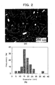
- Fig.2 shows 3C-SiC nanowhisker grown with Fe thin film of 24nm thickness and at substrate temperature of 900 °C.
- Fig.2(a) shows SEM(Scanning Electron Microscopy) image of the sample surface
- Fig.2(b) shows the distribution of diameters of the formed 3C-SiC nanowhiskers.
- the whole surface of Si substrate was covered with the 3C-SiC nanowhiskers, and its diameter was distributed in the range of 5 - 38.5 nm with the distribution peak at 15.4 nm.
- the density of 3C-SiC nanowhisker was uniform over the Si substrate surface. Its length was 1.5 - 2.1 micrometer. Its axis direction was nearly perpendicular to Si substrate surface.
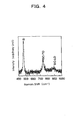
- Fig.3 shows TEM image and electron beam diffraction image of the whisker of the present invention measured by TEM.
- the whisker of the present invention has basically smooth surface and thin and long form. It was also seen that this whisker was almost straight and showed no bent or distortion. Most of these whiskers had cylindrical form with circular cross section, and some others had cylindrical form with cross sections of square, rectangle, triangle, and hexagon. However, all the whiskers of diameter 10nm or less had circular cross section.
- Fig.3(b) and (c) are the high magnitude TEM images of the whiskers with diameter 11nm and 45nm respectively. As is seen from these figures, these whiskers have the structure of single crystal 3C-SiC.
- the 200 diffraction spot in the diffraction pattern are a typical character of the 3C-SiC crystal structure owing to the asymmetric effect of the elements C and Si in the crystal lattice, because the 200 diffraction spot are forbidden or could arise weakly from double diffraction inhibiting rule of a single crystal like Si and diamond.
- nanowhisker formed on Si (100) substrate
- a series of samples were prepared by depositing Fe thin film with various film thickness and synthesizing at various substrate temperatures. It was found as the result that nanowhisker can be grown in the range of substrate temperature 800 - 1000°C, and with Fe thin film thickness 9 - 105 nm. The diameters of all the nanowhisker were smaller than the thickness of Fe thin film. 90 nanowhiskers were chosen from each of all the samples, their diameters were measured, the most frequently occuring diameter was determined, and the dependency of the most frequently occuring diameter on the substrate temperature and on the thickness of Fe thin film were obtained.
- Fig.5 shows the dependency on the substrate temperature and on the thickness of Fe thin film
- Fig.5(a) shows the dependency on the substrate temperature with constant Fe thin film thickness
- Fig.5(b) is the dependency on the thickness of Fe thin film at constant substrate temperature.
- the diameter which is 8nm at the substrate temperature 800 °C increases with increase of the temperature, reaches to its maximum 32nm at the temperature 950°C, and then decreases with increase of the temperature from 950°C to 1000°C, and the diameter increased monotonically from 9 nm to 58 nm with increase of the thickness of Fe thin film from 9 nm to 105 nm.
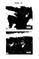
- Fig.6 shows the nanowhisker growing through the hole of Si substrate
- Fig.6(a) is SEM image of the sample surface
- Fig.6(b) is SEM image of the sample cross section. It can be seen from SEM image of the sample surface of Fig.6(a) that the root of nanowhisker is below Si substrate surface (shown by white arrow in the figure). It is also seen from SEM image of the sample cross section of Fig.6(b) that there are many holes and the whisker's roots are buried fairly deep from Si substrate surface.
- PL(Photo Luminescence) of 3C-SiC nanowhisker synthesized by the method of the present invention is explained below.
- Fig.7 is PL spectrum measured at room temperature, and the wavelength of its excited light was 325 nm.
- PL spectra designated as (a), (b), (c), (d), and (e) in the figure are those of the samples, respectively, of 3C-SiC nanowhiskers synthesized at substrate temperature 800, 850, 900, 950, and 1000°C.
- PL spectrum has more or less asymmetric shape, and broad distribution which can not be separated to several simple peaks.
- PL intensity is increased with increase of the substrate temperature.
- the increase of PL intensity mainly depend on the amount of 3C-SiC nanowhisker in the irradiation region of PL excited light.
- Fig.8 shows the relationship between PL peak energy and the diameter of 3C-SiC nanowhisker, and its abscissa is the diameter of 3C-SiC nanowhisker and ordinate is PL leak energy.
- PL peak energy shifts to blue with decreasing the diameter of 3C-SiC nanowhisker.
- the fact that PL peak energy varies monotonously with 3C-SiC nanowhisker diameter indicates the existence of quantum confinement effect.
- the two dimensional quantum confinement effect makes it possible the PL peak energy to exceed the band gap energy of 3C-SiC in bulk form.
- Forchel et al verified a blueshift of the PL peak for the lowest energy levels of a zincblend structure and rectangular cross-sectional whisker with a fixed side length of the rectangles, and proved that the quantum energy and consequently the energy gap between electron and hole level varied as E ⁇ 1/Lx 2 with whisker width Lx(Semicond. Sci. Technol. 11, 1529, 1996).
- E peak 2.16 + 32 d m0 -2 (eV) where d m0 is the most commonly occurring diameter of the 3C-SiC nanowhiskers in the sample.
- the PL peak energy may not exactly corresponds to the energy gap
- the first term 2.16 eV in the first term of Equation (1) is relatively close to the energy gap of 3C-SiC in bulk form. Equation (1) is quite useful for the manufacturing of the optoelectonic device which utilize the 3C-SiC nanowhisker.
- 3C-SiC nanowhisker firmly fixed on Si substrate can be synthesized densely with the controlled diameter and the length. According to the present invention, the 3C-SiC nanowhisker can be synthesized safely and at a low cost.
- the 3C-SiC nanowhisker of the present invention can be used as the light emitting source which is able to be manufactured by Si device manufacturing process. And extremely useful device can be formed, if the 3C-SiC nanowhisker light emitting device owing to quantum confinement effect and conventional Si device are formed on the same substrate.
Landscapes
- Chemical & Material Sciences (AREA)
- Organic Chemistry (AREA)
- Engineering & Computer Science (AREA)
- Crystallography & Structural Chemistry (AREA)
- Materials Engineering (AREA)
- Metallurgy (AREA)
- Inorganic Chemistry (AREA)
- General Chemical & Material Sciences (AREA)
- Chemical Kinetics & Catalysis (AREA)
- Nanotechnology (AREA)
- Physics & Mathematics (AREA)
- Composite Materials (AREA)
- Condensed Matter Physics & Semiconductors (AREA)
- General Physics & Mathematics (AREA)
- Crystals, And After-Treatments Of Crystals (AREA)
- Carbon And Carbon Compounds (AREA)
Abstract
Description
Claims (12)
- A synthesizing method of 3C-SiC nanowhisker, characterized in that it comprises the steps of:depositing a thin film made of a metal element or metal elements on Si substrate; andholding the substrate in a plasma consisting of hydrogen and hydrocarbon for a time period at a substrate temperature.
- A synthesizing method of 3C-SiC nanowhisker as set forth in claim 1, characterized in that said metal element is one or more elements selected from the group which consists of Fe, Co and Ni.
- A synthesizing method of 3C-SiC nanowhisker as set forth in claim 1 or 2, characterized in that a diameter of said 3C-SiC nanowhisker is controlled by controlling a thickness of said thin film.
- A synthesizing method of 3C-SiC nanowhisker as set forth in claim 1, characterized in that a length of said 3C-SiC whisker is controlled by controlling said time period and said substrate temperature.
- A synthesizing method of 3C-SiC nanowhisker as set forth in claim 1 or 2, characterized in that said metal element of said thin film is Fe, and said hydrocarbon is one selected from the group of paraffin hydrocarbon expressed as chemical formula CnH2n+2.
- A synthesizing method of 3C-SiC nanowhisker as set forth in claim 5, characterized in that a thickness of said thin film is any thickness between 5nm and 105 nm.
- A synthesizing method of 3C-SiC nanowhisker as set forth in claim 1, characterized in that said substrate temperature is within the range of 800 to 1100°C.
- A synthesizing method of 3C-SiC nanowhisker as set forth in claim 1 or 4, characterized in that said plasma is microwave plasma.
- A 3C-SiC nanowhisker, characterized in that it has:the chemical formula of SiC;the cubic crystal lattice; anda diameter of nanosize.
- A 3C-SiC nanowhisker as set forth in claim 9, characterized in that said diameter is any diameter between 8nm and 50 nm, and is uniform in a direction of said 3C-SiC nanowhisker axis.
- A 3C-SiC nanowhisker as set forth in claim 9, characterized in that a root of said 3C-SiC nanowhisker is buried and fixed in Si substrate, and said 3C-SiC nanowhisker is grown nearly perpendicular to a surface of said Si substrate.
- A 3C-SiC nanowhisker as set forth in claim 9, characterized in that a wavelength of emitted light of the 3C-SiC nanowhisker can be varied by the diameter thereof.
Applications Claiming Priority (3)
| Application Number | Priority Date | Filing Date | Title |
|---|---|---|---|
| JP2001191226 | 2001-06-25 | ||
| JP2001191226A JP3918073B2 (en) | 2001-06-25 | 2001-06-25 | Method for synthesizing 3C-SiC nanowhiskers and 3C-SiC nanowhiskers |
| PCT/JP2002/006236 WO2003000965A1 (en) | 2001-06-25 | 2002-06-21 | 3c-sic nanowhisker synthesizing method and 3c-sic nanowhisker |
Publications (2)
| Publication Number | Publication Date |
|---|---|
| EP1411155A1 true EP1411155A1 (en) | 2004-04-21 |
| EP1411155A4 EP1411155A4 (en) | 2008-07-02 |
Family
ID=19029883
Family Applications (1)
| Application Number | Title | Priority Date | Filing Date |
|---|---|---|---|
| EP02738776A Withdrawn EP1411155A4 (en) | 2001-06-25 | 2002-06-21 | PROCESS FOR SYNTHESIS OF 3C-SIC NANOWHISKERS AND 3C-SIC NANOWHISKERS |
Country Status (5)
| Country | Link |
|---|---|
| US (2) | US7364714B2 (en) |
| EP (1) | EP1411155A4 (en) |
| JP (1) | JP3918073B2 (en) |
| TW (1) | TWI296291B (en) |
| WO (1) | WO2003000965A1 (en) |
Cited By (1)
| Publication number | Priority date | Publication date | Assignee | Title |
|---|---|---|---|---|
| WO2019137942A1 (en) * | 2018-01-12 | 2019-07-18 | Universität Paderborn | Device and method for producing silicon carbide |
Families Citing this family (9)
| Publication number | Priority date | Publication date | Assignee | Title |
|---|---|---|---|---|
| EP1634334A1 (en) * | 2003-04-04 | 2006-03-15 | Startskottet 22286 AB | Nanowhiskers with pn junctions and methods of fabricating thereof |
| US20070189953A1 (en) * | 2004-01-30 | 2007-08-16 | Centre National De La Recherche Scientifique (Cnrs) | Method for obtaining carbon nanotubes on supports and composites comprising same |
| US7597814B2 (en) * | 2004-03-23 | 2009-10-06 | Hewlett Packard Development Company, L.P. | Structure formed with template having nanoscale features |
| KR100807081B1 (en) | 2005-10-22 | 2008-02-25 | 한국원자력연구원 | Selective growth method of one-dimensional silicon carbide deposition |
| US8067303B1 (en) * | 2006-09-12 | 2011-11-29 | Partial Assignment University of Central Florida | Solid state energy conversion device |
| US7754600B2 (en) * | 2007-03-01 | 2010-07-13 | Hewlett-Packard Development Company, L.P. | Methods of forming nanostructures on metal-silicide crystallites, and resulting structures and devices |
| JP2010241666A (en) * | 2009-03-31 | 2010-10-28 | Tokyo Institute Of Technology | Core-shell structure type silicon carbide nanowire and method for producing the same |
| JP2013540353A (en) * | 2010-09-29 | 2013-10-31 | エンパイア テクノロジー ディベロップメント エルエルシー | Phase change energy storage in ceramic nanotube composites |
| DE102018100681A1 (en) * | 2018-01-12 | 2019-07-18 | Universität Paderborn | Method for producing silicon carbide |
Family Cites Families (8)
| Publication number | Priority date | Publication date | Assignee | Title |
|---|---|---|---|---|
| JPS6236100A (en) | 1985-08-09 | 1987-02-17 | Ube Ind Ltd | Production of silicon carbide whisker |
| US5116679A (en) * | 1988-07-29 | 1992-05-26 | Alcan International Limited | Process for producing fibres composed of or coated with carbides or nitrides |
| FI82231C (en) * | 1988-11-30 | 1991-02-11 | Kemira Oy | FOERFARANDE FOER FRAMSTAELLNING AV KERAMRAOMATERIAL. |
| WO1992022922A2 (en) * | 1991-06-12 | 1992-12-23 | Case Western Reserve University | Process for the controlled growth of single-crystal films of silicon carbide polytypes on silicon carbide wafers |
| US5514350A (en) * | 1994-04-22 | 1996-05-07 | Rutgers, The State University Of New Jersey | Apparatus for making nanostructured ceramic powders and whiskers |
| JPH10203810A (en) * | 1997-01-21 | 1998-08-04 | Canon Inc | Manufacturing method of carbon nanotube |
| US5997832A (en) * | 1997-03-07 | 1999-12-07 | President And Fellows Of Harvard College | Preparation of carbide nanorods |
| US6221154B1 (en) * | 1999-02-18 | 2001-04-24 | City University Of Hong Kong | Method for growing beta-silicon carbide nanorods, and preparation of patterned field-emitters by chemical vapor depositon (CVD) |
-
2001
- 2001-06-25 JP JP2001191226A patent/JP3918073B2/en not_active Expired - Fee Related
-
2002
- 2002-06-21 EP EP02738776A patent/EP1411155A4/en not_active Withdrawn
- 2002-06-21 TW TW091113575A patent/TWI296291B/en not_active IP Right Cessation
- 2002-06-21 WO PCT/JP2002/006236 patent/WO2003000965A1/en not_active Ceased
- 2002-06-21 US US10/481,578 patent/US7364714B2/en not_active Expired - Fee Related
-
2007
- 2007-01-03 US US11/648,569 patent/US7521034B2/en not_active Expired - Fee Related
Cited By (1)
| Publication number | Priority date | Publication date | Assignee | Title |
|---|---|---|---|---|
| WO2019137942A1 (en) * | 2018-01-12 | 2019-07-18 | Universität Paderborn | Device and method for producing silicon carbide |
Also Published As
| Publication number | Publication date |
|---|---|
| US20080003162A1 (en) | 2008-01-03 |
| US7364714B2 (en) | 2008-04-29 |
| US7521034B2 (en) | 2009-04-21 |
| WO2003000965A1 (en) | 2003-01-03 |
| EP1411155A4 (en) | 2008-07-02 |
| JP3918073B2 (en) | 2007-05-23 |
| TWI296291B (en) | 2008-05-01 |
| US20050089680A1 (en) | 2005-04-28 |
| JP2003002800A (en) | 2003-01-08 |
Similar Documents
| Publication | Publication Date | Title |
|---|---|---|
| Xiang et al. | Green-light-emitting ZnSe nanowires fabricated via vapor phase growth | |
| Zhang et al. | Germanium nanowires sheathed with an oxide layer | |
| Zhang et al. | Diameter modification of silicon nanowires by ambient gas | |
| Zhang et al. | Fabrication and photoluminescence of ordered GaN nanowire arrays | |
| Tang et al. | Synthesis and characterization of single-crystal indium nitride nanowires | |
| Zhang et al. | Synthesis of 3C–SiC nanowhiskers and emission of visible photoluminescence | |
| Yang et al. | Fabrication of silicon-vacancy color centers in diamond films: tetramethylsilane as a new dopant source | |
| US7521034B2 (en) | 3C-SiC nanowhisker | |
| Xing et al. | Solid–liquid–solid (SLS) growth of coaxial nanocables: silicon carbide sheathed with silicon oxide | |
| Hassan et al. | Optical and structural studies of Ge nanocrystals embedded in AlN matrix fabricated by pulsed laser deposition | |
| Zhang et al. | Fabrication, structural characterization and optical properties of semiconducting gallium oxide nanobelts | |
| Opolchentsev et al. | UV luminescence and lasing in ensembles of zinc-oxide microcrystals with copper | |
| Yoo et al. | Fabrication and Optical Characteristics of Position‐Controlled ZnO Nanotubes and ZnO/Zn0. 8Mg0. 2O Coaxial Nanotube Quantum Structure Arrays | |
| Liu et al. | Size-controlled growth of ZnO nanowires by catalyst-free high-pressure pulsed laser deposition and their optical properties | |
| Reiser et al. | Controlled catalytic growth and characterization of zinc oxide nanopillars on a-plane sapphire | |
| Ursaki et al. | Optical characterization of hierarchical ZnO structures grown with a simplified vapour transport method | |
| Sedov et al. | Formation of Ge-V color centers in poly-and monocrystalline CVD diamond: A comparative study | |
| Kim et al. | Gallium oxide nanomaterials produced on SiO2 substrates via thermal evaporation | |
| JP4431745B2 (en) | Method for producing aluminum nitride nanoribbon | |
| Chang et al. | Modulation of luminescence emission spectra of N-doped ß-Ga2O3 nanowires by thermal evaporation | |
| Hamidinezhad et al. | Influence of growth time on morphology and structural properties of silicon nanowires grown by VHF-PECVD | |
| dengan Kaedah | Si Nanowires Produced by Very High Frequency Plasma Enhanced Chemical Vapor Deposition (PECVD) via VLS Mechanism | |
| Rizal et al. | Spectroscopic Characterization of Gallium Nitride Nanowires | |
| Silakhori et al. | Fabrication and photoluminescence of one dimensional AlN nanostructures for application as light emitting devices | |
| Zinovyev et al. | Structural and optical properties of two-dimensional Si and Ge layers formed by molecular beam epitaxy on CaF2/Si (111) substrates |
Legal Events
| Date | Code | Title | Description |
|---|---|---|---|
| PUAI | Public reference made under article 153(3) epc to a published international application that has entered the european phase |
Free format text: ORIGINAL CODE: 0009012 |
|
| 17P | Request for examination filed |
Effective date: 20040115 |
|
| AK | Designated contracting states |
Kind code of ref document: A1 Designated state(s): AT BE CH CY DE DK ES FI FR GB GR IE IT LI LU MC NL PT SE TR |
|
| RIN1 | Information on inventor provided before grant (corrected) |
Inventor name: ZHANG, YAFEI Inventor name: GAMO, MIKA Inventor name: ANDO, TOSHIHIRO |
|
| RIN1 | Information on inventor provided before grant (corrected) |
Inventor name: ANDO, TOSHIHIRO Inventor name: ZHANG, YAFEI C/ORESEARCH INSTITUTE FOR MICRO/NANOM Inventor name: GAMO, MIKA |
|
| A4 | Supplementary search report drawn up and despatched |
Effective date: 20080603 |
|
| 17Q | First examination report despatched |
Effective date: 20090608 |
|
| STAA | Information on the status of an ep patent application or granted ep patent |
Free format text: STATUS: THE APPLICATION IS DEEMED TO BE WITHDRAWN |
|
| 18D | Application deemed to be withdrawn |
Effective date: 20120103 |