EP1408610A1 - Ring oscillator with a digitally programmable frequency - Google Patents
Ring oscillator with a digitally programmable frequency Download PDFInfo
- Publication number
- EP1408610A1 EP1408610A1 EP20030255857 EP03255857A EP1408610A1 EP 1408610 A1 EP1408610 A1 EP 1408610A1 EP 20030255857 EP20030255857 EP 20030255857 EP 03255857 A EP03255857 A EP 03255857A EP 1408610 A1 EP1408610 A1 EP 1408610A1
- Authority
- EP
- European Patent Office
- Prior art keywords
- tri
- coupled
- ring oscillator
- inverting stage
- state
- Prior art date
- Legal status (The legal status is an assumption and is not a legal conclusion. Google has not performed a legal analysis and makes no representation as to the accuracy of the status listed.)
- Withdrawn
Links
- 230000007246 mechanism Effects 0.000 claims abstract description 4
- 238000000034 method Methods 0.000 claims description 15
- 239000004065 semiconductor Substances 0.000 claims description 9
- 239000000758 substrate Substances 0.000 claims 2
- 230000008569 process Effects 0.000 description 6
- 230000000295 complement effect Effects 0.000 description 4
- 238000004519 manufacturing process Methods 0.000 description 4
- 230000008859 change Effects 0.000 description 1
- 230000003247 decreasing effect Effects 0.000 description 1
- 229940073619 encare Drugs 0.000 description 1
- 230000006870 function Effects 0.000 description 1
- 230000003993 interaction Effects 0.000 description 1
- 238000012986 modification Methods 0.000 description 1
- 230000004048 modification Effects 0.000 description 1
Images


Classifications
-
- H—ELECTRICITY
- H03—ELECTRONIC CIRCUITRY
- H03K—PULSE TECHNIQUE
- H03K3/00—Circuits for generating electric pulses; Monostable, bistable or multistable circuits
- H03K3/02—Generators characterised by the type of circuit or by the means used for producing pulses
- H03K3/027—Generators characterised by the type of circuit or by the means used for producing pulses by the use of logic circuits, with internal or external positive feedback
- H03K3/03—Astable circuits
- H03K3/0315—Ring oscillators
Definitions
- the present invention relates to digital circuits. More specifically, the present invention relates to a method and an apparatus for digitally programming a frequency for a ring oscillator.
- Digital circuits typically operate under control of a system clock signal that is used to synchronize interactions between circuit elements. Because of the simplicity of its design, a ring oscillator is often used to generate such a clock signal.
- a ring oscillator comprises an odd number of inverting stages connected into a ring.
- ring oscillator 103 on semiconductor chip 102 includes five inverters 104-108 connected input-to-output to form a ring in which the output of the last inverter 108 feeds back into the input of the first inverter 104.
- this circuit produces a clock signal that oscillates with a period equal to twice the gate delay of each inverting stage multiplied by the number of inverting stages. For example, if each of the five inverters 104-108 in FIG. 1 has a one-nanosecond delay, ring oscillator 103 will oscillate with a period of 10 nanoseconds.
- the clock frequency of a digital system can be decreased during latent periods of operation in order to decrease the power consumption of the digital circuit.
- a number of ring oscillator designs allow the number of inverting stages in the ring oscillator to be adjusted through fuses or semiconductor switches. For example, see U.S. Patent No. 5,689,213, entitled “Post-Fabrication Programmable Integrated Circuit Ring Oscillator,” by inventor Joseph C. Sher, filed on August 23, 1995 and issued on November 18, 1997. However, in these designs, inverting stages must be added or removed from the ring oscillator in pairs. This means that only coarse frequency adjustments are possible using this technique.
- one embodiment of the present invention provides a ring oscillator with a digitally programmable frequency.
- This ring oscillator includes an odd number of inverting stages coupled input to output to form a ring, and a programming mechanism configured to digitally program the drive strength for each inverting stage in the ring oscillator, thereby changing the propagation delay between inverting stages and thereby allowing the frequency of the ring oscillator to be adjusted.
- a given inverting stage includes a plurality of tri-state inverters coupled in parallel, so that the inputs of the tri-state inverters are coupled to a common input for the given inverting stage, and the outputs of the tri-state inverters are coupled to a common output for the given inverting stage.
- each of the tri-state inverters can be selectively enabled, thereby allowing the drive strength of the given inverting stage to be adjusted.
- the tri-state inverters for the given inverting stage have equal drive strength, so that enabling additional tri-state inverters increases the drive strength of the given inverting stage linearly.
- the tri-state inverters for the given inverting stage may have different gate lengths and hence different drive strengths.
- the tri-state inverters for the given inverting stage may have drive strengths that vary by powers of two, so that the drive strength of the given inverting stage can be digitally programmed with a binary number.
- a tri-state inverter in the given inverting stage includes: a first P-type transistor with a source coupled to V DD , and a gate coupled to the input of the tri-state inverter; a second P-type transistor with a source coupled to the drain of the first P-type transistor, a gate coupled to an enable signal for the tri-state inverter and a drain coupled to the output of the tri-state inverter; a first N-type transistor with a drain coupled to the output of the tri-state inverter, and a gate coupled to the inverse of the enable signal; and a second N-type transistor with a drain coupled to the source of the first N-type transistor, a gate coupled to the input of the tri-state inverter and a source coupled to ground.
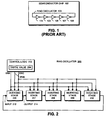
- FIG. 2 illustrates a ring oscillator 200 with a programmable frequency in accordance with one embodiment of the present invention.
- the ring oscillator 200 illustrated in FIG. 2 includes five inverting stages 206-210. However, in general any odd number of inverting stages can be used.
- Ring oscillator 200 additionally includes control logic 202, which holds a digital value 204 corresponding to a frequency for ring oscillator 200.
- Control logic 202 uses digital value 204 to generate a set of enable signals, ENA, ENB and ENC, which feed into inverting stages 206-210. These enable signals ENA, ENB and ENC are used to selectively enable tri-state inverters that are coupled together in parallel within inverting stages 206-210.
- FIG. 2 does not show complementary enable signals ENA_L, ENB_L and ENC_L that accompany enable signals ENA, ENB and ENC.
- control logic 202 can generally include any type of state machine, programmable Read-Only Memory (ROM), or other type of control mechanism that can be used to generate enable signals for inverting stages 206-210.
- control logic 202 is able to adjust the drive strength for each inverting stage in ring oscillator 200. This changes the propagation delay between inverting stages 206-210 and thereby allows the frequency of ring oscillator 200 to be adjusted. This adjustment process is described in more detail below with reference to FIGs. 3-6.
- FIG. 3 illustrates an implementation of inverting stage 206 within ring oscillator 200 in accordance with one embodiment of the present invention.
- inverting stage 206 receives an input signal 212 and generates an inverted output signal 214 (see FIG. 2).
- inverting stage 206 in FIG. 3 includes three tri-state inverters connected in parallel. Note that in general inverting stage 206 can include any number of tri-state inverters connected in parallel, and is not limited to the three parallel tri-state inverters illustrated in FIG. 3.
- a first tri-state inverter 320 in inverting stage 206 includes P-type transistors 302 and 305 as well as N-type transistors 308 and 311, which are coupled in series between V DD and ground.
- enable signal ENA is asserted to a low voltage
- complementary enable signal ENA_L is asserted to V DD
- P-type transistor 305 and N-type transistor 308 become transparent. This allows P-type transistor 302 and N-type transistor 311 to invert input signal 212 to produce output signal 214.
- a second tri-state inverter 321 includes P-type transistors 303 and 306 as well as N-type transistors 309, and 312, which are coupled in series between V DD and ground. Tri-state inverter 321 can similarly be enabled by asserting enable signal ENB to a low voltage and asserting complementary enable signal ENB_L to V DD .
- a third tri-state inverter 322 includes P-type transistors 304 and 307 as well as N-type transistors 310 and 313, which are coupled in series between V DD and ground. Tri-state inverter 322 can also be enabled by asserting enable signal ENC to a low voltage and asserting complementary enable signal ENC_L to V DD .
- the drive strengths of inverters 320, 321 and 322 are all the same. In this case, enabling additional inverters increases the drive strength of inverting stage 206 linearly. Note the drive strength for a given tri-state inverter can be adjusted prior to manufacture by adjusting the gate widths of the transistors in the given tri-state inverter.
- the drive strengths of inverters 320, 321 and 322 vary by successive by powers of two.
- the drive strength of the second inverter 321 can be twice the drive strength of the first inverter 320
- the drive strength of the third inverter 322 can be twice the drive strength of the second inverter 321.
- a three digit binary value can be used to selectively enable different combinations of inverters 320, 321 and 322 to produce a corresponding drive strength that is proportional to the three digit binary value.
- FIG. 4 illustrates an alternative implementation of inverting stage 206 in accordance with another embodiment of the present invention.
- This alternative implementation is the same as the implementation illustrated in FIG. 3, except that the drains of P-type transistors 302-304 have been coupled together at terminal 323, and the drains of N-type transistors 311-313 have been coupled together at terminal 324.
- P-type transistors 302-303 and N-type transistors 311-313 always remain active.
- enable signals ENA, ENB and ENC determine the resistance between terminal 323 and output terminal 214
- enable signals ENA_L, ENB_L, and ENC_L determine the resistance between terminal 324 and output terminal 214.
- enable signals ENA, ENA_L, ENB, ENB_L, ENC, and ENC_L determine the drive strength of inverting stage 206.
- FIG. 5 illustrates yet another implementation of inverting stage 206 in accordance with another embodiment of the present invention.
- This implementation is a variation on the embodiment illustrated in FIG. 4 in which the three parallel P-type transistors 302-304 are replaced be a single P-type transistor 325, and the three parallel N-type transistors 311-313 are replaced by a single N-type transistor 326.
- This embodiment operates in generally the same way as the embodiment illustrated in FIG. 4, wherein enable signals ENA, ENB, and ENC determine the resistance between terminal 323 and output 214, and enable signals ENA_L, ENB_L, and ENC_L determine the resistance between terminal 324 and output terminal 214. This allows enable signals ENA, ENA_L, ENB, ENB_L, ENC, and ENC_L to determine the drive strength of inverting stage 206.
- enable signals illustrated in FIGs. 3-5 are "active low,” which means that they are asserted with a low voltage, the present invention is not limited to circuits with active low enable signals. Equivalent circuitry which makes use of "active high” enable signals can also be used.
- FIG. 6 is a flow chart of a process for configuring the frequency of a ring oscillator in accordance with one embodiment of the present invention.
- the process starts when control logic 202 produces a digital value 204 composed of a series of ones and zeros associated with a specific frequency for ring oscillator 200 (see FIG. 2) (step 602).
- This digital value 204 can be received from an external source, can be programmed, or can be generated internally by control logic 202.
- control logic 202 uses digital value 204 to program the drive strength for the inverting stages by asserting enable signals ENA, ENA_L, ENB, ENB_L, ENC and ENC_L (step 604). This can involve performing a function on digital value 204 to compute enable signals ENA, ENA_L, ENB, ENB_L, ENC and ENC_L. Ring oscillator 200 is then able to operate at the selected frequency (step 606).
Landscapes
- Pulse Circuits (AREA)
Abstract
One embodiment of the present invention provides a ring oscillator with a
digitally programmable frequency. This ring oscillator includes an odd number of
inverting stages coupled input to output to form a ring, and a programming
mechanism configured to digitally program the drive strength for each inverting
stage in the ring oscillator, thereby changing the propagation delay between
inverting stages and thereby allowing the frequency of the ring oscillator to be
adjusted. The given inverting stage may include a plurality of tri-state inverters
coupled in parallel, so that inputs of the tri-state inverters are coupled to a
common input for the given inverting stage, and outputs of the tri-state inverters
are coupled to a common output for the given inverting stage. Each of the tri-state
inverters can be selectively enabled, thereby allowing the drive strength of the
given inverting stage to be adjusted.
Description
- The present invention relates to digital circuits. More specifically, the present invention relates to a method and an apparatus for digitally programming a frequency for a ring oscillator.
- Digital circuits typically operate under control of a system clock signal that is used to synchronize interactions between circuit elements. Because of the simplicity of its design, a ring oscillator is often used to generate such a clock signal.
- A ring oscillator comprises an odd number of inverting stages connected into a ring. For example, referring to FIG. 1,
ring oscillator 103 onsemiconductor chip 102 includes five inverters 104-108 connected input-to-output to form a ring in which the output of the last inverter 108 feeds back into the input of the first inverter 104. - Assuming that each inverting stage is identical, this circuit produces a clock signal that oscillates with a period equal to twice the gate delay of each inverting stage multiplied by the number of inverting stages. For example, if each of the five inverters 104-108 in FIG. 1 has a one-nanosecond delay,
ring oscillator 103 will oscillate with a period of 10 nanoseconds. - It is often useful to be able to dynamically change the clock frequency of a digital system. For example, the clock frequency can be decreased during latent periods of operation in order to decrease the power consumption of the digital circuit. Furthermore, it is often desirable to fine tune circuitry after fabrication to achieve a desired clock speed. Note that variations in the processes used to manufacture semiconductor chips often cause substantial variations in propagation delay through circuit elements. It is therefore not possible to determine how fast a digital circuit will operate before it is manufactured. Hence, it is typically necessary to fine tune a digital circuit after it is manufactured to achieve a desired frequency.
- A number of ring oscillator designs allow the number of inverting stages in the ring oscillator to be adjusted through fuses or semiconductor switches. For example, see U.S. Patent No. 5,689,213, entitled "Post-Fabrication Programmable Integrated Circuit Ring Oscillator," by inventor Joseph C. Sher, filed on August 23, 1995 and issued on November 18, 1997. However, in these designs, inverting stages must be added or removed from the ring oscillator in pairs. This means that only coarse frequency adjustments are possible using this technique.
- Accordingly, one embodiment of the present invention provides a ring oscillator with a digitally programmable frequency. This ring oscillator includes an odd number of inverting stages coupled input to output to form a ring, and a programming mechanism configured to digitally program the drive strength for each inverting stage in the ring oscillator, thereby changing the propagation delay between inverting stages and thereby allowing the frequency of the ring oscillator to be adjusted.
- In one embodiment, a given inverting stage includes a plurality of tri-state inverters coupled in parallel, so that the inputs of the tri-state inverters are coupled to a common input for the given inverting stage, and the outputs of the tri-state inverters are coupled to a common output for the given inverting stage. Moreover, each of the tri-state inverters can be selectively enabled, thereby allowing the drive strength of the given inverting stage to be adjusted.
- In one particular embodiment, the tri-state inverters for the given inverting stage have equal drive strength, so that enabling additional tri-state inverters increases the drive strength of the given inverting stage linearly. Alternatively, the tri-state inverters for the given inverting stage may have different gate lengths and hence different drive strengths. For example, the tri-state inverters for the given inverting stage may have drive strengths that vary by powers of two, so that the drive strength of the given inverting stage can be digitally programmed with a binary number.
- In one particular embodiment, a tri-state inverter in the given inverting stage includes: a first P-type transistor with a source coupled to VDD, and a gate coupled to the input of the tri-state inverter; a second P-type transistor with a source coupled to the drain of the first P-type transistor, a gate coupled to an enable signal for the tri-state inverter and a drain coupled to the output of the tri-state inverter; a first N-type transistor with a drain coupled to the output of the tri-state inverter, and a gate coupled to the inverse of the enable signal; and a second N-type transistor with a drain coupled to the source of the first N-type transistor, a gate coupled to the input of the tri-state inverter and a source coupled to ground.
- Various embodiments of the invention will now be described in detail by way of example only with reference to the following drawings:
- FIG. 1 illustrates a ring oscillator on a semiconductor chip.
- FIG. 2 illustrates a ring oscillator with a programmable frequency in accordance with one embodiment of the present invention.
- FIG. 3 illustrates an implementation of a stage in a ring oscillator in accordance with one embodiment of the present invention.
- FIG. 4 illustrates an alternative implementation of a stage in a ring oscillator in accordance with one embodiment of the present invention.
- FIG. 5 illustrates yet another implementation of a stage in a ring oscillator in accordance with one embodiment of the present invention.
- FIG. 6 is a flow chart of the process of configuring the frequency of a ring oscillator in accordance with one embodiment of the present invention.
-
- FIG. 2 illustrates a
ring oscillator 200 with a programmable frequency in accordance with one embodiment of the present invention. Thering oscillator 200 illustrated in FIG. 2 includes five inverting stages 206-210. However, in general any odd number of inverting stages can be used. -
Ring oscillator 200 additionally includescontrol logic 202, which holds adigital value 204 corresponding to a frequency forring oscillator 200.Control logic 202 usesdigital value 204 to generate a set of enable signals, ENA, ENB and ENC, which feed into inverting stages 206-210. These enable signals ENA, ENB and ENC are used to selectively enable tri-state inverters that are coupled together in parallel within inverting stages 206-210. Note that FIG. 2 does not show complementary enable signals ENA_L, ENB_L and ENC_L that accompany enable signals ENA, ENB and ENC. Also note thatcontrol logic 202 can generally include any type of state machine, programmable Read-Only Memory (ROM), or other type of control mechanism that can be used to generate enable signals for inverting stages 206-210. - By selectively enabling tri-state drivers in inverting stages 206-210,
control logic 202 is able to adjust the drive strength for each inverting stage inring oscillator 200. This changes the propagation delay between inverting stages 206-210 and thereby allows the frequency ofring oscillator 200 to be adjusted. This adjustment process is described in more detail below with reference to FIGs. 3-6. - FIG. 3 illustrates an implementation of inverting
stage 206 withinring oscillator 200 in accordance with one embodiment of the present invention. During operation, invertingstage 206 receives aninput signal 212 and generates an inverted output signal 214 (see FIG. 2). - The implementation of inverting
stage 206 in FIG. 3 includes three tri-state inverters connected in parallel. Note that ingeneral inverting stage 206 can include any number of tri-state inverters connected in parallel, and is not limited to the three parallel tri-state inverters illustrated in FIG. 3. - As is illustrated in FIG. 3, a first tri-state
inverter 320 in invertingstage 206 includes P-type transistors type transistors type transistor 305 and N-type transistor 308 become transparent. This allows P-type transistor 302 and N-type transistor 311 to invertinput signal 212 to produceoutput signal 214. - A second tri-state
inverter 321 includes P-type transistors type transistors Tri-state inverter 321 can similarly be enabled by asserting enable signal ENB to a low voltage and asserting complementary enable signal ENB_L to VDD. - Finally, a
third tri-state inverter 322 includes P-type transistors type transistors inverter 322 can also be enabled by asserting enable signal ENC to a low voltage and asserting complementary enable signal ENC_L to VDD. - By selectively enabling different combinations of tri-state
inverters stage 206. In one embodiment of the present invention, the drive strengths ofinverters stage 206 linearly. Note the drive strength for a given tri-state inverter can be adjusted prior to manufacture by adjusting the gate widths of the transistors in the given tri-state inverter. - In another embodiment of the present invention, the drive strengths of
inverters second inverter 321 can be twice the drive strength of thefirst inverter 320, and the drive strength of thethird inverter 322 can be twice the drive strength of thesecond inverter 321. In this way, a three digit binary value can be used to selectively enable different combinations ofinverters - FIG. 4 illustrates an alternative implementation of inverting
stage 206 in accordance with another embodiment of the present invention. This alternative implementation is the same as the implementation illustrated in FIG. 3, except that the drains of P-type transistors 302-304 have been coupled together atterminal 323, and the drains of N-type transistors 311-313 have been coupled together atterminal 324. In this embodiment, P-type transistors 302-303 and N-type transistors 311-313 always remain active. - Moreover, enable signals ENA, ENB and ENC determine the resistance between
terminal 323 andoutput terminal 214, and enable signals ENA_L, ENB_L, and ENC_L determine the resistance betweenterminal 324 andoutput terminal 214. In this way, enable signals ENA, ENA_L, ENB, ENB_L, ENC, and ENC_L determine the drive strength of invertingstage 206. - FIG. 5 illustrates yet another implementation of inverting
stage 206 in accordance with another embodiment of the present invention. This implementation is a variation on the embodiment illustrated in FIG. 4 in which the three parallel P-type transistors 302-304 are replaced be a single P-type transistor 325, and the three parallel N-type transistors 311-313 are replaced by a single N-type transistor 326. This embodiment operates in generally the same way as the embodiment illustrated in FIG. 4, wherein enable signals ENA, ENB, and ENC determine the resistance betweenterminal 323 andoutput 214, and enable signals ENA_L, ENB_L, and ENC_L determine the resistance betweenterminal 324 andoutput terminal 214. This allows enable signals ENA, ENA_L, ENB, ENB_L, ENC, and ENC_L to determine the drive strength of invertingstage 206. - Although the enable signals illustrated in FIGs. 3-5 are "active low," which means that they are asserted with a low voltage, the present invention is not limited to circuits with active low enable signals. Equivalent circuitry which makes use of "active high" enable signals can also be used.
- FIG. 6 is a flow chart of a process for configuring the frequency of a ring oscillator in accordance with one embodiment of the present invention. The process starts when
control logic 202 produces adigital value 204 composed of a series of ones and zeros associated with a specific frequency for ring oscillator 200 (see FIG. 2) (step 602). Thisdigital value 204 can be received from an external source, can be programmed, or can be generated internally bycontrol logic 202. - Next,
control logic 202 usesdigital value 204 to program the drive strength for the inverting stages by asserting enable signals ENA, ENA_L, ENB, ENB_L, ENC and ENC_L (step 604). This can involve performing a function ondigital value 204 to compute enable signals ENA, ENA_L, ENB, ENB_L, ENC and ENC_L.Ring oscillator 200 is then able to operate at the selected frequency (step 606). - Although the present invention has been described in the context of the implementations illustrated in FIGs. 2-6, the present invention is not meant to be limited to these specific implementations. For example, any suitable technique for varying the drive strength of inverting stages in a ring oscillator based on a digital input may be used.
- The foregoing descriptions of embodiments of the present invention have been presented for purposes of illustration in order to enable a person skilled in the art to appreciate and implement the invention. They are provided in the context of particular applications and their requirements, but are not intended to be exhaustive or to limit the present invention to the forms disclosed. Accordingly, many modifications and variations will be apparent to practitioners skilled in the art, and the scope of the present invention is defined by the appended claims.
Claims (15)
- A ring oscillator with a digitally programmable frequency, comprising:an odd number of inverting stages coupled input to output to form a ring; anda programming mechanism configured to digitally program the drive strength for each inverting stage in the ring oscillator, thereby changing the propagation delay between inverting stages to allow the frequency of the ring oscillator to be adjusted.
- The ring oscillator of claim 1, wherein a given inverting stage includes:wherein each of the tri-state inverters can be selectively enabled, to allow the drive strength of the given inverting stage to be adjusted.a plurality of tri-state inverters coupled in parallel, so that the inputs of the tri-state inverters are coupled to a common input for the given inverting stage, and the outputs of the tri-state inverters are coupled to a common output for the given inverting stage;
- The ring oscillator of claim 2, wherein the tri-state inverters for the given inverting stage have equal drive strength, so that enabling additional tri-state inverters increases the drive strength of the given inverting stage linearly.
- The ring oscillator of claim 2, wherein the tri-state inverters for the given inverting stage have different gate lengths and hence different drive strengths.
- The ring oscillator of claim 4, wherein the tri-state inverters for the given inverting stage have drive strengths that vary by powers of two, so that the drive strength of the given inverting stage can be digitally programmed with a binary number.
- The ring oscillator of any of claims 2 to 5, wherein a tri-state inverter in the given inverting stage includes:a first P-type transistor with a source coupled to VDD, and a gate coupled to the input of the tri-state inverter;a second P-type transistor with a source coupled to the drain of the first P-type transistor, a gate coupled to an enable signal for the tri-state inverter and a drain coupled to the output of the tri-state inverter;a first N-type transistor with a drain coupled to the output of the tri-state inverter, and a gate coupled to the inverse of the enable signal; anda second N-type transistor with a drain coupled to the source of the first N-type transistor, a gate coupled to the input of the tri-state inverter and a source coupled to ground.
- A method for digitally programming a frequency of a ring oscillator, wherein the ring oscillator includes an odd number of inverting stages coupled input to output to form a ring, comprising:wherein programming the drive strength changes the propagation delay between inverting stages and thereby adjusts the frequency of the ring oscillator.receiving a digital value associated with the frequency for the ring oscillator; andusing the digital value to program a drive strength for each inverting stage in the ring oscillator;
- The method of claim 7, wherein a given inverting stage includes:wherein each of the tri-state inverters can be selectively enabled, thereby allowing the drive strength of the given inverting stage to be adjusted.a plurality of tri-state inverters coupled in parallel, so that the inputs of the tri-state inverters are coupled to a common input for the given inverting stage, and the outputs of the tri-state inverters are coupled to a common output for the given inverting stage;
- The method of claim 8, wherein the tri-state inverters for the given inverting stage have equal drive strength, so that enabling additional tri-state inverters increases the drive strength of the given inverting stage linearly.
- The method of claim 8, wherein the tri-state inverters for the given inverting stage have different gate lengths and hence different drive strengths.
- The method of claim 10, wherein the tri-state inverters for the given inverting stage have drive strengths that vary by powers of two, so that the drive strength of the given inverting stage can be digitally programmed with a binary number.
- The method of any of claims 8 to 11, wherein a tri-state inverter in the given inverting stage includes:a first P-type transistor with a source coupled to VDD, and a gate coupled to the input of the tri-state inverter;a second P-type transistor with a source coupled to the drain of the first P-type transistor, a gate coupled to an enable signal for the tri-state inverter and a drain coupled to the output of the tri-state inverter;a first N-type transistor with a drain coupled to the output of the tri-state inverter, and a gate coupled to the inverse of the enable signal; anda second N-type transistor with a drain coupled to the source of the first N-type transistor, a gate coupled to the input of the tri-state inverter and a source coupled to ground.
- A semiconductor chip comprising:a semiconductor substrate;a ring oscillator on the semiconductor substrate according to any of claims 1 to 6.
- The semiconductor chip of claim 13, wherein the semiconductor chip includes a central processing unit.
- A computer system comprising:a processor;a memory;a ring oscillator according to any of claims 1 to 6.
Applications Claiming Priority (2)
| Application Number | Priority Date | Filing Date | Title |
|---|---|---|---|
| US269338 | 1994-06-30 | ||
| US10/269,338 US6825732B2 (en) | 2002-10-11 | 2002-10-11 | Ring oscillator with a digitally programmable frequency |
Publications (1)
| Publication Number | Publication Date |
|---|---|
| EP1408610A1 true EP1408610A1 (en) | 2004-04-14 |
Family
ID=32030382
Family Applications (1)
| Application Number | Title | Priority Date | Filing Date |
|---|---|---|---|
| EP20030255857 Withdrawn EP1408610A1 (en) | 2002-10-11 | 2003-09-18 | Ring oscillator with a digitally programmable frequency |
Country Status (3)
| Country | Link |
|---|---|
| US (1) | US6825732B2 (en) |
| EP (1) | EP1408610A1 (en) |
| TW (1) | TW200419909A (en) |
Families Citing this family (16)
| Publication number | Priority date | Publication date | Assignee | Title |
|---|---|---|---|---|
| US7069525B2 (en) * | 2003-07-18 | 2006-06-27 | International Business Machines Corporation | Method and apparatus for determining characteristics of MOS devices |
| US7336134B1 (en) * | 2004-06-25 | 2008-02-26 | Rf Micro Devices, Inc. | Digitally controlled oscillator |
| US7548127B2 (en) * | 2006-04-11 | 2009-06-16 | International Rectifier Corporation | Digitally controlled ring oscillator |
| US7429897B1 (en) * | 2006-08-31 | 2008-09-30 | Altera Corporation | Wide operating-frequency range voltage controlled oscillators |
| US8217635B2 (en) * | 2009-04-03 | 2012-07-10 | Infineon Technologies Ag | LDO with distributed output device |
| US8378753B2 (en) * | 2010-05-07 | 2013-02-19 | Macronix International Co., Ltd. | Oscillator with frequency determined by relative magnitudes of current sources |
| US9000822B2 (en) | 2013-04-09 | 2015-04-07 | International Business Machines Corporation | Programmable delay circuit |
| US10103719B2 (en) * | 2013-07-22 | 2018-10-16 | Nvidia Corporation | Integrated voltage regulator with in-built process, temperature and aging compensation |
| US9628059B2 (en) | 2015-06-18 | 2017-04-18 | International Business Machines Corporation | Fine delay structure with programmable delay ranges |
| US10469060B1 (en) * | 2017-12-22 | 2019-11-05 | The Boeing Company | Synchronizable ring oscillators |
| US10469059B1 (en) * | 2017-12-22 | 2019-11-05 | The Boeing Company | Stabilizing the startup behavior of ring oscillators |
| US10615785B1 (en) * | 2019-03-21 | 2020-04-07 | Qualcomm Incorporated | Fully compensated complementary duty cycle correction circuits |
| JP6847160B2 (en) | 2019-06-11 | 2021-03-24 | 華邦電子股▲ふん▼有限公司Winbond Electronics Corp. | Ring oscillator and time measurement circuit |
| TWI692202B (en) * | 2019-06-13 | 2020-04-21 | 華邦電子股份有限公司 | Ringing oscillator and time measuring circuit |
| CN112332839B (en) * | 2020-11-05 | 2024-03-01 | 北京奕斯伟计算技术股份有限公司 | Voltage controlled oscillator, control method thereof, P2P interface circuit and electronic equipment |
| US12388450B2 (en) * | 2023-09-27 | 2025-08-12 | Logistics and Supply Chain MultiTech R&D Centre Limited | Electronic oscillator circuit and a method for controlling an oscillation frequency of a ring oscillator circuit |
Citations (2)
| Publication number | Priority date | Publication date | Assignee | Title |
|---|---|---|---|---|
| US6204694B1 (en) * | 1999-05-21 | 2001-03-20 | Logicvision, Inc. | Programmable clock signal generation circuits and methods for generating accurate, high frequency, clock signals |
| US6272439B1 (en) * | 1998-02-24 | 2001-08-07 | Vlsi Technology, Inc. | Programmable delay path circuit and operating point frequency detection apparatus |
Family Cites Families (4)
| Publication number | Priority date | Publication date | Assignee | Title |
|---|---|---|---|---|
| US4517532A (en) * | 1983-07-01 | 1985-05-14 | Motorola, Inc. | Programmable ring oscillator |
| US4988960A (en) * | 1988-12-21 | 1991-01-29 | Yamaha Corporation | FM demodulation device and FM modulation device employing a CMOS signal delay device |
| US5689213A (en) * | 1995-08-23 | 1997-11-18 | Micron Technology, Inc. | Post-fabrication programmable integrated circuit ring oscillator |
| US6359477B1 (en) * | 1999-06-03 | 2002-03-19 | Texas Instruments Incorporated | Low power driver design |
-
2002
- 2002-10-11 US US10/269,338 patent/US6825732B2/en not_active Expired - Lifetime
-
2003
- 2003-09-18 EP EP20030255857 patent/EP1408610A1/en not_active Withdrawn
- 2003-10-09 TW TW092128116A patent/TW200419909A/en unknown
Patent Citations (2)
| Publication number | Priority date | Publication date | Assignee | Title |
|---|---|---|---|---|
| US6272439B1 (en) * | 1998-02-24 | 2001-08-07 | Vlsi Technology, Inc. | Programmable delay path circuit and operating point frequency detection apparatus |
| US6204694B1 (en) * | 1999-05-21 | 2001-03-20 | Logicvision, Inc. | Programmable clock signal generation circuits and methods for generating accurate, high frequency, clock signals |
Also Published As
| Publication number | Publication date |
|---|---|
| TW200419909A (en) | 2004-10-01 |
| US20040070459A1 (en) | 2004-04-15 |
| US6825732B2 (en) | 2004-11-30 |
Similar Documents
| Publication | Publication Date | Title |
|---|---|---|
| US6825732B2 (en) | Ring oscillator with a digitally programmable frequency | |
| US5497263A (en) | Variable delay circuit and clock signal supply unit using the same | |
| US8130016B2 (en) | Techniques for providing reduced duty cycle distortion | |
| US6600355B1 (en) | Clock generator circuit providing an output clock signal from phased input clock signals | |
| CN101355350B (en) | Phase shift circuit with lower intrinsic delay | |
| JP2951802B2 (en) | Clock generation circuit | |
| US20040150447A1 (en) | Duty-cycle adjustable buffer and method and method for operating same | |
| US7196561B2 (en) | Programmable reset signal that is independent of supply voltage ramp rate | |
| CN103004089A (en) | Integrated Circuits with Dual Edge Clocks | |
| US20050162208A1 (en) | Delay generator | |
| US7573339B2 (en) | Ring oscillator with ultra-wide frequency tuning range | |
| EP0701323A2 (en) | Resistorless voltage controlled oscillator | |
| CN108809276A (en) | Digitally Controlled Delay Line | |
| US8159277B1 (en) | Techniques for providing multiple delay paths in a delay circuit | |
| US20010013101A1 (en) | Delay adjustment circuit and a clock generating circuit using the same | |
| EP0924859A1 (en) | Self-clocked logic circuit and methodology | |
| JP4512158B2 (en) | Variable delay network | |
| US20240213961A1 (en) | Clock adjustment circuit with bias scheme | |
| US7388442B2 (en) | Digitally controlled oscillator for reduced power over process variations | |
| JP2611034B2 (en) | Delay circuit | |
| JP2006515096A (en) | Circuit and method for generating a clock signal | |
| US6788124B1 (en) | Method and apparatus for reducing jitter in a delay line and a trim unit | |
| US20130200937A1 (en) | Delay line with cell by cell power down capability | |
| US7437584B2 (en) | Apparatus and method for reducing power consumption in electronic devices | |
| JP2012239185A (en) | Integrated circuit comprising signal skew adjustment cell selected from cell library |
Legal Events
| Date | Code | Title | Description |
|---|---|---|---|
| PUAI | Public reference made under article 153(3) epc to a published international application that has entered the european phase |
Free format text: ORIGINAL CODE: 0009012 |
|
| AK | Designated contracting states |
Kind code of ref document: A1 Designated state(s): AT BE BG CH CY CZ DE DK EE ES FI FR GB GR HU IE IT LI LU MC NL PT RO SE SI SK TR |
|
| AX | Request for extension of the european patent |
Extension state: AL LT LV MK |
|
| 17P | Request for examination filed |
Effective date: 20040930 |
|
| AKX | Designation fees paid |
Designated state(s): DE GB |
|
| 17Q | First examination report despatched |
Effective date: 20050322 |
|
| STAA | Information on the status of an ep patent application or granted ep patent |
Free format text: STATUS: THE APPLICATION IS DEEMED TO BE WITHDRAWN |
|
| 18D | Application deemed to be withdrawn |
Effective date: 20050802 |