EP1408579A1 - Low noise block down converter with a plurality of local oscillators - Google Patents
Low noise block down converter with a plurality of local oscillators Download PDFInfo
- Publication number
- EP1408579A1 EP1408579A1 EP03018144A EP03018144A EP1408579A1 EP 1408579 A1 EP1408579 A1 EP 1408579A1 EP 03018144 A EP03018144 A EP 03018144A EP 03018144 A EP03018144 A EP 03018144A EP 1408579 A1 EP1408579 A1 EP 1408579A1
- Authority
- EP
- European Patent Office
- Prior art keywords
- electromagnetic coupling
- low noise
- local oscillators
- down converter
- dielectric resonators
- Prior art date
- Legal status (The legal status is an assumption and is not a legal conclusion. Google has not performed a legal analysis and makes no representation as to the accuracy of the status listed.)
- Granted
Links
- 230000008878 coupling Effects 0.000 claims abstract description 25
- 238000010168 coupling process Methods 0.000 claims abstract description 25
- 238000005859 coupling reaction Methods 0.000 claims abstract description 25
- 239000002184 metal Substances 0.000 claims abstract description 23
- 230000010355 oscillation Effects 0.000 claims description 8
- 239000000758 substrate Substances 0.000 claims description 8
- 230000005672 electromagnetic field Effects 0.000 description 5
- 230000004048 modification Effects 0.000 description 4
- 238000012986 modification Methods 0.000 description 4
- 230000000052 comparative effect Effects 0.000 description 2
- 238000010586 diagram Methods 0.000 description 2
- 230000002452 interceptive effect Effects 0.000 description 1
- 230000002265 prevention Effects 0.000 description 1
- 239000000523 sample Substances 0.000 description 1
- 230000005236 sound signal Effects 0.000 description 1
Images




Classifications
-
- H—ELECTRICITY
- H01—ELECTRIC ELEMENTS
- H01P—WAVEGUIDES; RESONATORS, LINES, OR OTHER DEVICES OF THE WAVEGUIDE TYPE
- H01P1/00—Auxiliary devices
- H01P1/20—Frequency-selective devices, e.g. filters
- H01P1/207—Hollow waveguide filters
- H01P1/208—Cascaded cavities; Cascaded resonators inside a hollow waveguide structure
- H01P1/2084—Cascaded cavities; Cascaded resonators inside a hollow waveguide structure with dielectric resonators
-
- H—ELECTRICITY
- H01—ELECTRIC ELEMENTS
- H01Q—ANTENNAS, i.e. RADIO AERIALS
- H01Q1/00—Details of, or arrangements associated with, antennas
- H01Q1/12—Supports; Mounting means
- H01Q1/22—Supports; Mounting means by structural association with other equipment or articles
- H01Q1/24—Supports; Mounting means by structural association with other equipment or articles with receiving set
- H01Q1/247—Supports; Mounting means by structural association with other equipment or articles with receiving set with frequency mixer, e.g. for direct satellite reception or Doppler radar
Definitions
- the present invention generally relates to a low noise block down converter. More particularly, the present invention relates to a low noise block down converter utilized for a satellite reception system.
- each local oscillator is completely separated from another local oscillator by a metal wall in order to prevent electromagnetic coupling between a dielectric resonator in each local oscillator and a dielectric resonator in another local oscillator.
- LNB Low Noise Block down converter
- Figs. 7A and 7B are cross-sectional views showing a main portion of the conventional LNB.
- Fig. 7A is a cross-sectional view cut along a line VIIA-VIIA in Fig. 7B
- Fig. 7B is a cross-sectional view cut along a line VIIB-VIIB in Fig. 7A.
- two local oscillators 41a and 41b of the LNB are respectively housed within shielding chambers 40a and 40b in a metal shielding box 40, and are electromagnetically shielded by a metal wall 40c.
- Local oscillator 41a includes a dielectric resonator 42a, an oscillation device 43a, a microstrip line 44a, and a substrate 45a.
- Local oscillator 41a outputs a signal of a certain frequency (e.g. 9.75 GHz).
- Local oscillator 41b includes a dielectric resonator 42b, an oscillation device 43b, a microstrip line 44b, and a substrate 45b.
- Local oscillator 41b outputs a signal of another frequency (e.g. 10.6 GHz).
- dashed circles show electromagnetic fields radiated from dielectric resonators 42a and 42b.
- metal shielding box 40 is divided by metal wall 40c to prevent electromagnetic coupling between dielectric resonators 42a and 42b. Therefore, downsizing of metal shielding box 40 and hence the low noise block down converter has been difficult to achieve.
- An object of the present invention is to provide a compact low noise block down converter.
- a low noise block down converter includes a plurality of local oscillators each including a dielectric resonator and having an oscillation frequency different from each other, an electromagnetic coupling preventing member preventing electromagnetic coupling between one of the dielectric resonators and another one of the dielectric resonators, and a metal shielding box including one shielding chamber accommodating the plurality of local oscillators and the electromagnetic coupling preventing member. Therefore, the metal shielding box and hence the low noise block down converter can be made small compared to the conventional case in which the plurality of local oscillators are completely separated from each other by a metal wall.
- the electromagnetic coupling preventing member includes a conductive bar having one end extending between any two of the dielectric resonators and receiving a reference potential.
- the conductive bar can prevent the electromagnetic coupling between the two dielectric resonators.
- the low noise block down converter includes a substrate having a surface on which the plurality of local oscillators are mounted.
- the electromagnetic coupling preventing member includes a conductive pattern formed on the surface of the substrate between any two of the dielectric resonators and receiving a reference potential. In this case, the conductive pattern can prevent the electromagnetic coupling between the two dielectric resonators.
- the electromagnetic coupling preventing member further includes a metal plate provided between any two of the dielectric resonators and receiving a reference potential.
- the metal plate can prevent the electromagnetic coupling between the two dielectric resonators.
- a satellite reception system in accordance with an embodiment of the present invention includes a broadcasting satellite 1, an antenna 2, an LNB 3, an IF (Intermediate Frequency) cable 4, a DBS (Direct Broadcasting Satellite) tuner 5, and a television 6.
- IF Intermediate Frequency
- DBS Direct Broadcasting Satellite
- a radio wave in a 12 GHz band (10.70-12.75 GHz) transmitted from broadcasting satellite 1 is received by antenna 2.
- the received radio wave is frequency-converted to an IF signal in a 1 GHz band (950-2150 MHz) and low-noise amplified by LNB 3 mounted to antenna 2.
- the IF signal output from LNB 3 is introduced indoors via IF cable 4, demodulated into a video and audio signal by DBS tuner 5, and then transmitted to television 6.
- universal LNB 3 includes a waveguide 10, a Low Noise Amplifier (hereinafter referred to as an "LNA”) 11, a Band Pass Filter (hereinafter referred to as a "BPF") 12, local oscillators 13a and 13b, a mixer 14, an IF amplifier 15, a power supply unit 16, condensers 17a and 17b, a coil 18, and an output terminal 19.
- LNA Low Noise Amplifier
- BPF Band Pass Filter
- a vertically polarized wave signal and a horizontally polarized wave signal in the 12 GHz band (10.70-12.75 GHz) transmitted from broadcasting satellite 1 are respectively received at two antenna probes in waveguide 10.
- the received signals are low-noise amplified by LNA 11, and then input to BPF 12.
- BPF 12 a signal in an image frequency band is removed to produce a signal in a desired frequency band.
- the signal output from BPF 12 is mixed with a local oscillation signal (9.75 GHz) from local oscillator 13a or with a local oscillation signal (10.6 GHz) from local oscillator 13b by mixer 14, and is frequency-converted to the IF signal in the 1 GHz band (950 to 2150 MHz). Two local oscillators 13a and 13b may be switched therebetween for use.
- the IF signal output from mixer 14 is amplified to have appropriate noise characteristics and gain characteristics by IF amplifier 15, condensers 17a and 17b, and coil 18, and is output from output terminal 19. It is noted that LNA 11, local oscillators 13a and 13b, and IF amplifier 15 are powered through power supply unit 16.
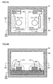
- Figs. 3A and 3B are cross-sectional views showing the configuration of two local oscillators 13a and 13b shown in Fig. 2.
- Fig. 3A is a cross-sectional view cut along a line IIIA-IIIA in Fig. 3B
- Fig. 3B is a cross-sectional view cut along a line IIIB-IIIB in Fig. 3A.
- a substrate 24 with two local oscillators 13a and 13b mounted thereon and a conductive bar 25 are housed within one shielding chamber 20a in a metal shielding box 20.
- Local oscillator 13a includes a dielectric resonator 21a, an oscillation device 22a, and a microstrip line 23a.
- Local oscillator 13a outputs the signal at the frequency of 9.75 GHz.
- Local oscillator 13b includes a dielectric resonator 21b, an oscillation device 22b, and a microstrip line 23b.
- Local oscillator 13b outputs the signal at the frequency of 10.6 GHz.
- a proximal end of conductive bar 25 is bonded to the middle of a ceiling of metal shielding box 20.
- a distal end of conductive bar 25 extends between two dielectric resonators 21a and 21b.
- Conductive bar 25 and metal shielding box 20 are grounded.
- Conductive bar 25 prevents coupling of electromagnetic fields (dashed circles in Fig. 3B) radiated from two dielectric resonators 21a and 21b.
- Figs. 4A and 4B are cross-sectional views showing a comparative example for the present embodiment.
- Fig. 4A is a cross-sectional view cut along a line IVA-IVA in Fig. 4B
- Fig. 4B is a cross-sectional view cut along a line IVB-IVB in Fig. 4A.
- the configuration shown in Figs. 4A and 4B is different from the configuration shown in Figs. 3A and 3B in that conductive bar 25 is not provided between dielectric resonators 21a and 21b.
- electromagnetic fields dasheshed circles in Fig. 4B
- radiated from two dielectric resonators 21a and 21b are coupled to each other. This results in local oscillators 13a and 13b interfering with each other and failing to produce signals at the desired frequencies (9.75 GHz, 10.6 GHz).
- the electromagnetic coupling between two dielectric resonators 21a and 21b is prevented by conductive bar 25. Therefore, metal shielding box 20 and hence the LNB can be smaller compared to the conventional case in which the electromagnetic coupling between two dielectric resonators 21a and 21b is prevented by metal wall 40c.
- two local oscillators 13a and 13b are provided within one shielding chamber 20a in metal shielding box 20.
- electromagnetic coupling can be prevented even when a plurality of local oscillators are provided in shielding chamber 20a, as long as conductive bar 25 is provided for each space between adjacent local oscillators.
- Figs. 5A and 5B are cross-sectional views showing a modification of the present embodiment.
- the configuration shown in Figs. 5A and 5B is different from the configuration shown in Figs. 4A and 4B in that a ground pattern 26 is formed on substrate 24 between dielectric resonators 21a and 21b and that ground pattern 26 is connected to metal shielding box 20 via a through hole 27.
- ground pattern 26 and through hole 27 prevent coupling between electromagnetic fields (dashed circles in Fig. 5B) radiated from two dielectric resonators 21a and 21b.
- Figs. 6A and 6B are cross-sectional views showing another modification of the present embodiment.
- the configuration shown in Figs. 6A and 6B is different from the configuration shown in Figs. 5A and 5B in that a metal plate 28 is provided on ground pattern 26.
- ground pattern 26, through hole 27, and metal plate 28 prevent coupling between electromagnetic fields (dashed circles in Fig. 6B) radiated from two dielectric resonators 21a and 21b. Therefore, more ensured prevention of the electromagnetic coupling between two dielectric resonators 21a and 21b can be achieved.
Landscapes
- Engineering & Computer Science (AREA)
- Radar, Positioning & Navigation (AREA)
- Remote Sensing (AREA)
- Input Circuits Of Receivers And Coupling Of Receivers And Audio Equipment (AREA)
- Structure Of Receivers (AREA)
- Two-Way Televisions, Distribution Of Moving Picture Or The Like (AREA)
- Shielding Devices Or Components To Electric Or Magnetic Fields (AREA)
- Control Of Motors That Do Not Use Commutators (AREA)
Abstract
Description
Claims (4)
- A low noise block down converter, comprising:a plurality of local oscillators (13a, 13b) each including a dielectric resonator (21a, 21b) and having an oscillation frequency different from each other;an electromagnetic coupling preventing member (25-28) preventing electromagnetic coupling between one and another one of said dielectric resonators (21a, 21b); anda metal shielding box (20) including one shielding chamber (20a) accommodating said plurality of local oscillators (13a, 13b) and said electromagnetic coupling preventing member (25-28).
- The low noise block down converter according to claim 1, wherein said electromagnetic coupling preventing member (25-28) includes a conductive bar (25) having one end extending between any two of said dielectric resonators (21a, 21b) and receiving a reference potential.
- The low noise block down converter according to claim 1, further comprising a substrate (24) having a surface on which said plurality of local oscillators (13a, 13b) are mounted, wherein
said electromagnetic coupling preventing member (25-28) includes a conductive pattern (26) formed on the surface of said substrate (24) between any two of said dielectric resonators (21a, 21b) and receiving a reference potential. - The low noise block down converter according to claim 1, wherein said electromagnetic coupling preventing member (25-28) includes a metal plate (28) provided between any two of said dielectric resonators (21a, 21b) and receiving a reference potential.
Applications Claiming Priority (2)
| Application Number | Priority Date | Filing Date | Title |
|---|---|---|---|
| JP2002296157A JP3923405B2 (en) | 2002-10-09 | 2002-10-09 | Low noise converter |
| JP2002296157 | 2002-10-09 |
Publications (2)
| Publication Number | Publication Date |
|---|---|
| EP1408579A1 true EP1408579A1 (en) | 2004-04-14 |
| EP1408579B1 EP1408579B1 (en) | 2006-11-29 |
Family
ID=32025537
Family Applications (1)
| Application Number | Title | Priority Date | Filing Date |
|---|---|---|---|
| EP03018144A Expired - Lifetime EP1408579B1 (en) | 2002-10-09 | 2003-08-08 | Low noise block down converter with a plurality of local oscillators |
Country Status (5)
| Country | Link |
|---|---|
| US (1) | US7177618B2 (en) |
| EP (1) | EP1408579B1 (en) |
| JP (1) | JP3923405B2 (en) |
| CN (1) | CN1254930C (en) |
| DE (1) | DE60310007T2 (en) |
Families Citing this family (5)
| Publication number | Priority date | Publication date | Assignee | Title |
|---|---|---|---|---|
| DE602004010157T2 (en) * | 2003-09-18 | 2008-10-30 | Thomson Licensing | Bidirectional wide-distribution user terminal with configurable radiated frequencies |
| JP4533035B2 (en) * | 2004-08-02 | 2010-08-25 | キヤノン株式会社 | Image encoding apparatus and method, computer program, and computer-readable storage medium |
| TWI271027B (en) * | 2005-02-14 | 2007-01-11 | Wistron Neweb Corp | LNBF and shielding structure thereof |
| JP2014064237A (en) * | 2012-09-24 | 2014-04-10 | Sharp Corp | Satellite communication or satellite broadcast reception apparatus, and low noise converter used therefor |
| JP6083214B2 (en) * | 2012-11-30 | 2017-02-22 | セイコーエプソン株式会社 | Oscillator, electronic device, and moving object |
Citations (6)
| Publication number | Priority date | Publication date | Assignee | Title |
|---|---|---|---|---|
| US4691378A (en) * | 1984-12-24 | 1987-09-01 | Sony Corporation | Tuner for television receiver |
| JPH01152800A (en) * | 1987-12-10 | 1989-06-15 | Matsushita Electric Ind Co Ltd | Case for high-frequency instrument |
| EP0718964A2 (en) * | 1994-12-20 | 1996-06-26 | Fujitsu Compound Semiconductor, Inc. | Switchable oscillator circuit and method |
| JPH1098311A (en) * | 1996-09-20 | 1998-04-14 | Fujitsu General Ltd | Microwave equipment |
| US6271603B1 (en) * | 1998-07-16 | 2001-08-07 | Alps Electric Co., Ltd. | Frequency conversion apparatus |
| JP2002246924A (en) * | 2001-02-21 | 2002-08-30 | Sharp Corp | Satellite broadcasting receiver |
Family Cites Families (22)
| Publication number | Priority date | Publication date | Assignee | Title |
|---|---|---|---|---|
| US5008956A (en) * | 1987-09-30 | 1991-04-16 | Conifer Corporation | Interdigital local oscillator filter apparatus |
| US4922211A (en) * | 1988-04-15 | 1990-05-01 | Siemens Aktiengesellschaft | Microwave oscillator in which the dielectric resonator is hermetically sealed |
| US5125109A (en) * | 1988-06-23 | 1992-06-23 | Comsat | Low noise block down-converter for direct broadcast satellite receiver integrated with a flat plate antenna |
| US5046135A (en) * | 1989-11-30 | 1991-09-03 | John E. Chance & Associates | Method and apparatus for frequency stabilization of a down converter |
| JPH04151906A (en) | 1990-10-15 | 1992-05-25 | Matsushita Electric Works Ltd | Microwave oscillator |
| JPH0522028A (en) | 1991-07-11 | 1993-01-29 | Nippon Telegr & Teleph Corp <Ntt> | Antenna device |
| JPH0553331A (en) | 1991-08-29 | 1993-03-05 | Nec Corp | Formation of fine pattern |
| JPH05191112A (en) | 1992-01-14 | 1993-07-30 | Tdk Corp | Shielding device for triplate line |
| JP3020401B2 (en) * | 1993-12-24 | 2000-03-15 | シャープ株式会社 | Converter circuit |
| US5483663A (en) * | 1994-04-05 | 1996-01-09 | Diversified Communication Engineering, Inc. | System for providing local originating signals with direct broadcast satellite television signals |
| EP0683561A1 (en) * | 1994-05-18 | 1995-11-22 | Guan-Wu Wang | Low-cost low noise block down-converter with a self-oscillating mixer for satellite broadcast receivers |
| JPH0946133A (en) * | 1995-07-31 | 1997-02-14 | Matsushita Electric Ind Co Ltd | Microwave oscillator circuit and down converter using the circuit |
| US5995818A (en) * | 1996-07-30 | 1999-11-30 | Trw Inc. | Low noise block downconverter |
| JPH1098310A (en) | 1996-09-24 | 1998-04-14 | Fujitsu Ltd | High frequency line |
| US5761605A (en) * | 1996-10-11 | 1998-06-02 | Northpoint Technology, Ltd. | Apparatus and method for reusing satellite broadcast spectrum for terrestrially broadcast signals |
| FR2777700B1 (en) * | 1998-04-20 | 2000-07-07 | Org Europeenne Telecommunications Par Satellite Eutelsat | FREQUENCY CONVERTER ARRANGEMENT FOR PARABOLIC ANTENNAS |
| US6538533B1 (en) * | 1999-04-09 | 2003-03-25 | Nec Tokin Corporation | Dielectric resonator filter |
| JP3629433B2 (en) | 2001-02-21 | 2005-03-16 | シャープ株式会社 | Satellite broadcast receiver |
| JP2003273762A (en) * | 2002-03-19 | 2003-09-26 | Sharp Corp | Converter structure in Universal LNB |
| JP2003309480A (en) * | 2002-04-15 | 2003-10-31 | Sharp Corp | Low noise converter |
| US6975837B1 (en) * | 2003-01-21 | 2005-12-13 | The Directv Group, Inc. | Method and apparatus for reducing interference between terrestrially-based and space-based broadcast systems |
| US6967619B2 (en) * | 2004-01-08 | 2005-11-22 | Kvh Industries, Inc. | Low noise block |
-
2002
- 2002-10-09 JP JP2002296157A patent/JP3923405B2/en not_active Expired - Fee Related
-
2003
- 2003-08-08 DE DE60310007T patent/DE60310007T2/en not_active Expired - Lifetime
- 2003-08-08 EP EP03018144A patent/EP1408579B1/en not_active Expired - Lifetime
- 2003-08-18 US US10/642,494 patent/US7177618B2/en not_active Expired - Fee Related
- 2003-10-09 CN CN200310100768.8A patent/CN1254930C/en not_active Expired - Fee Related
Patent Citations (6)
| Publication number | Priority date | Publication date | Assignee | Title |
|---|---|---|---|---|
| US4691378A (en) * | 1984-12-24 | 1987-09-01 | Sony Corporation | Tuner for television receiver |
| JPH01152800A (en) * | 1987-12-10 | 1989-06-15 | Matsushita Electric Ind Co Ltd | Case for high-frequency instrument |
| EP0718964A2 (en) * | 1994-12-20 | 1996-06-26 | Fujitsu Compound Semiconductor, Inc. | Switchable oscillator circuit and method |
| JPH1098311A (en) * | 1996-09-20 | 1998-04-14 | Fujitsu General Ltd | Microwave equipment |
| US6271603B1 (en) * | 1998-07-16 | 2001-08-07 | Alps Electric Co., Ltd. | Frequency conversion apparatus |
| JP2002246924A (en) * | 2001-02-21 | 2002-08-30 | Sharp Corp | Satellite broadcasting receiver |
Non-Patent Citations (3)
| Title |
|---|
| PATENT ABSTRACTS OF JAPAN vol. 013, no. 413 (E - 820) 12 September 1989 (1989-09-12) * |
| PATENT ABSTRACTS OF JAPAN vol. 1998, no. 09 31 July 1998 (1998-07-31) * |
| PATENT ABSTRACTS OF JAPAN vol. 2002, no. 12 12 December 2002 (2002-12-12) * |
Also Published As
| Publication number | Publication date |
|---|---|
| JP3923405B2 (en) | 2007-05-30 |
| US7177618B2 (en) | 2007-02-13 |
| CN1497870A (en) | 2004-05-19 |
| CN1254930C (en) | 2006-05-03 |
| JP2004134949A (en) | 2004-04-30 |
| DE60310007D1 (en) | 2007-01-11 |
| DE60310007T2 (en) | 2007-06-21 |
| US20040072550A1 (en) | 2004-04-15 |
| EP1408579B1 (en) | 2006-11-29 |
Similar Documents
| Publication | Publication Date | Title |
|---|---|---|
| US6700462B2 (en) | Microstrip line filter combining a low pass filter with a half wave bandpass filter | |
| US7046969B2 (en) | Miniaturized transmitter-receiver unit | |
| US5995818A (en) | Low noise block downconverter | |
| US7177618B2 (en) | Low noise block down converter with a plurality of local oscillators | |
| US8818319B2 (en) | Signal distribution and filtering in low noise block downconverters | |
| US7046982B2 (en) | High frequency device having a frame with segmented compartments for prevented unwanted signal propagation | |
| US20070238436A1 (en) | Radio reception apparatus receiving multiple radio signals different in frequency | |
| JP3905334B2 (en) | Receiver | |
| US6950644B2 (en) | Satellite broadcast receiving device having two local oscillation circuits and reduced spurious signal | |
| JP3530171B2 (en) | Transceiver | |
| JP2007103610A (en) | Electronic equipment | |
| KR20030010857A (en) | Dual feeding system for receiving satellite broadcasting signal | |
| JPH11177206A (en) | Semiconductor component mounting method and semiconductor circuit created by this mounting method | |
| KR960000142B1 (en) | Mutual interference avoidance device for vertical and horizontal input probes | |
| US6838948B2 (en) | Oscillation apparatus and communication apparatus using the same | |
| KR100391919B1 (en) | Dual mode oscillator with one dielectric resonator | |
| JP2001060889A (en) | LNB equipment | |
| KR910000694Y1 (en) | Jammer elimination circuit for ARM BG and Sekam L common tuners | |
| JP2003204279A (en) | Converter for satellite broadcasting reception | |
| JPH10209669A (en) | Shield structure for high frequency apparatus unit | |
| JP2003244005A (en) | Low noise converter | |
| JP2001102802A (en) | Converter for satellite broadcasting reception | |
| JP2009017112A (en) | Shielding structure, satellite broadcast receiving converter having shielding structure, and satellite broadcasting receiving antenna apparatus having shielding structure | |
| JP2007142712A (en) | High frequency apparatus | |
| JP2007104224A (en) | Tuner unit |
Legal Events
| Date | Code | Title | Description |
|---|---|---|---|
| PUAI | Public reference made under article 153(3) epc to a published international application that has entered the european phase |
Free format text: ORIGINAL CODE: 0009012 |
|
| AK | Designated contracting states |
Kind code of ref document: A1 Designated state(s): AT BE BG CH CY CZ DE DK EE ES FI FR GB GR HU IE IT LI LU MC NL PT RO SE SI SK TR |
|
| AX | Request for extension of the european patent |
Extension state: AL LT LV MK |
|
| 17P | Request for examination filed |
Effective date: 20040901 |
|
| 17Q | First examination report despatched |
Effective date: 20041014 |
|
| AKX | Designation fees paid |
Designated state(s): DE FR GB |
|
| GRAP | Despatch of communication of intention to grant a patent |
Free format text: ORIGINAL CODE: EPIDOSNIGR1 |
|
| GRAS | Grant fee paid |
Free format text: ORIGINAL CODE: EPIDOSNIGR3 |
|
| GRAA | (expected) grant |
Free format text: ORIGINAL CODE: 0009210 |
|
| AK | Designated contracting states |
Kind code of ref document: B1 Designated state(s): DE FR GB |
|
| REG | Reference to a national code |
Ref country code: GB Ref legal event code: FG4D |
|
| REF | Corresponds to: |
Ref document number: 60310007 Country of ref document: DE Date of ref document: 20070111 Kind code of ref document: P |
|
| ET | Fr: translation filed | ||
| PLBE | No opposition filed within time limit |
Free format text: ORIGINAL CODE: 0009261 |
|
| STAA | Information on the status of an ep patent application or granted ep patent |
Free format text: STATUS: NO OPPOSITION FILED WITHIN TIME LIMIT |
|
| 26N | No opposition filed |
Effective date: 20070830 |
|
| PGFP | Annual fee paid to national office [announced via postgrant information from national office to epo] |
Ref country code: FR Payment date: 20090814 Year of fee payment: 7 |
|
| PGFP | Annual fee paid to national office [announced via postgrant information from national office to epo] |
Ref country code: DE Payment date: 20090806 Year of fee payment: 7 Ref country code: GB Payment date: 20090805 Year of fee payment: 7 |
|
| GBPC | Gb: european patent ceased through non-payment of renewal fee |
Effective date: 20100808 |
|
| REG | Reference to a national code |
Ref country code: FR Ref legal event code: ST Effective date: 20110502 |
|
| REG | Reference to a national code |
Ref country code: DE Ref legal event code: R119 Ref document number: 60310007 Country of ref document: DE Effective date: 20110301 |
|
| PG25 | Lapsed in a contracting state [announced via postgrant information from national office to epo] |
Ref country code: FR Free format text: LAPSE BECAUSE OF NON-PAYMENT OF DUE FEES Effective date: 20100831 Ref country code: DE Free format text: LAPSE BECAUSE OF NON-PAYMENT OF DUE FEES Effective date: 20110301 |
|
| PG25 | Lapsed in a contracting state [announced via postgrant information from national office to epo] |
Ref country code: GB Free format text: LAPSE BECAUSE OF NON-PAYMENT OF DUE FEES Effective date: 20100808 |