EP1408549A1 - Process for manufacturing an array of cells including selection bipolar junction transistors - Google Patents
Process for manufacturing an array of cells including selection bipolar junction transistors Download PDFInfo
- Publication number
- EP1408549A1 EP1408549A1 EP02425604A EP02425604A EP1408549A1 EP 1408549 A1 EP1408549 A1 EP 1408549A1 EP 02425604 A EP02425604 A EP 02425604A EP 02425604 A EP02425604 A EP 02425604A EP 1408549 A1 EP1408549 A1 EP 1408549A1
- Authority
- EP
- European Patent Office
- Prior art keywords
- regions
- doping level
- region
- conductivity type
- active area
- Prior art date
- Legal status (The legal status is an assumption and is not a legal conclusion. Google has not performed a legal analysis and makes no representation as to the accuracy of the status listed.)
- Granted
Links
Images


Classifications
-
- H—ELECTRICITY
- H10—SEMICONDUCTOR DEVICES; ELECTRIC SOLID-STATE DEVICES NOT OTHERWISE PROVIDED FOR
- H10D—INORGANIC ELECTRIC SEMICONDUCTOR DEVICES
- H10D48/00—Individual devices not covered by groups H10D1/00 - H10D44/00
- H10D48/30—Devices controlled by electric currents or voltages
- H10D48/32—Devices controlled by only the electric current supplied, or only the electric potential applied, to an electrode which does not carry the current to be rectified, amplified or switched
- H10D48/366—Multistable devices; Devices having two or more distinct operating states
-
- H—ELECTRICITY
- H10—SEMICONDUCTOR DEVICES; ELECTRIC SOLID-STATE DEVICES NOT OTHERWISE PROVIDED FOR
- H10B—ELECTRONIC MEMORY DEVICES
- H10B63/00—Resistance change memory devices, e.g. resistive RAM [ReRAM] devices
- H10B63/10—Phase change RAM [PCRAM, PRAM] devices
Definitions
- the present invention relates to a process for manufacturing an array of cells including selection bipolar junction transistors.
- the invention refers to a memory array of a phase change memory (PCM) device, without being limited thereto.
- PCM phase change memory
- phase change memory cells utilize a class of materials that have the unique property of being reversibly switcheable from one phase to another with measurable distinct resistivity.
- Specific materials that may be suitably used in phase change memory cells are alloys of elements of the VI group of the periodic table as Te or Se, also called chalcogenides or chalcogenic materials.
- chalcogenides also called chalcogenic materials.
- a thin film of chalcogenic material may be employed as a programmable resistor, switching between a high and a low resistance condition.
- the use of chalcogenic storage elements has been already proposed to form a memory cell.
- the chalcogenic element is generally coupled with a selection element, generally a MOS transistor or a diode.
- the memory array 1 of Figure 1 comprises a plurality of memory cells 2, each including a storage element 3 of the phase change type and a selection element 4 formed here as a diode.
- the memory cells 2 are arranged on rows and columns.
- the storage element 3 has a first terminal connected to an own bit line BLn-1, BLn, BLn+1, ..., and a second terminal connected to an anode of the diode 4;
- the diode 4 has a cathode connected to an own word line WLn-1, WLn, WLn+1, ....
- bit line connected to the addressed cell is biased at a high voltage V OP and all the other (unselected) bit lines BLn-1, BLn+1, ... are grounded.
- word line connected to the addressed cell is grounded and all the other (unselected) word lines WLn-1, WLn+1, ... are biased at V CC , so that only the diode 4 connected to the selected word line and bit line is on.
- CMOS compatible processes for manufacturing PCM have been already proposed, wherein the diodes are integrated in a P-type substrate wherein N-type regions are formed.
- the N-type regions, defining the cathode of the diodes, are contacted by a metal line and form wordlines of the array.
- the N-type regions accommodate P-type regions that define the anodes of the diodes and are connected to long stripes of chalchogenic material at small portions thereof defining the storage elements.
- the stripes of chalchogenic material extend perpendicular to the wordlines and define bitlines of the array.
- the diodes are associated with parasitic bipolar transistors having emitters formed by the diode anodes and connected to the bitlines (here, bitline BLn); bases formed by the diode cathodes and connected to the wordlines (here, wordline WLn); and collectors formed by the substrate.
- bitlines here, bitline BLn
- wordline WLn wordline WLn
- collectors formed by the substrate The equivalent electric diagram of a real cell is shown of Figure 2.
- the bipolar transistor Since in known memory arrays the bipolar transistor is not exploited, but instead it is considered a parasitic element, its design is not optimized, so that its current gain ⁇ F is much less than 1, the current flowing in the selected wordline is about the same as the total emitter current (1.6-3.2 mA, as above discussed); this current flows along the entire wordline and in the pull-down transistor of the row decoder, causing an unacceptable voltage drop.
- Another solution of the above problem resides in maximizing the current gain ⁇ F , so as to minimize the current flowing in the selected wordline and the pull-down transistor; thereby reducing the dimensions of the local driver or conversely the number of the local drivers to two or four, each local driver driving four bits.
- the manufacture of a bipolar transistor as a selection element in a memory array with low current gain implies some problems.
- the process should be such as to avoid any possible shorting of the emitters and the base contacts in case of misalignments, even when the cell pitch is particularly tight.
- a high current gain requires a very low base doping, leading to a high base resistance. Since the base is also the wordline of the array, both delay time and voltage drop along the wordline would be increased. Not least, a high current flowing into the substrate can give rise to injection problems that must be carefully handled. All these problems require an accurate optimization of the manufacturing process and a tradeoff between conflicting requirements.
- Aim of this invention is to provide a manufacturing method allowing integration of a bipolar transistor in a cell array so as to overcome the above indicated drawbacks.
- the bipolar transistor operating as a selection element of an array of memory cells is formed in a semiconductor body including some distinct regions: a substrate of P-type; a subcollector region, of P-type, overlying the substrate; a collector region of P-type, overlying the subcollector region; a base region, of N-type, overlying the collector region; an emitter region, of P-type, housed in the base region; and a base contact.
- the emitter region and the base contact are contacted through contacts formed in a dielectric layer grown over the semiconductor body and are implanted after depositing the dielectric layer, or at least a lower portion thereof and opening the contacts, using an own mask. Thereby no misalignment of the emitter and base contact masks may cause short-circuits between the emitter and base contact regions.
- the doping of each of the regions forming the bipolar transistors is optimized as regards driving capability, leakage immunity, and low voltage requirement.
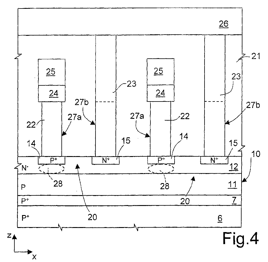
- a memory array is formed in a body 10 of semiconductor material including a heavily doped substrate 6 of P-type.
- the epitaxial layer also houses a plurality of active area strips 12, of N-type, defining base regions. The active area strips 12 extend parallel to each other along a first direction (X-direction) and are electrically insulated from each other by field oxide regions 13 ( Figure 5).
- Each active area strip 12 accommodates a plurality of emitter regions 14, of P + -type, and a plurality of base contact regions 15, of N + -type, that are arranged alternately, that is each emitter region 14 is arranged between two base contact regions 15, and each base contact region 15 is arranged between two emitter regions 14.
- each pair of regions including an emitter region 14 and the adjacent base contact region 15 (for example, an emitter region 14 and the base contact region 15 arranged on right thereof), the active area strip 12 they are accommodated in, and the underlying common collector region 11 form a selection transistor 20 of PNP-type, corresponding to bipolar transistor 4 of Figure 1.
- a dielectric region 21 extends on the body 10 and accommodates contacts, storage elements and interconnection lines.
- the dielectric region 21 is generally formed by more layers deposited subsequently to allow forming the various regions therein and may also include different materials.
- First and second contacts 22, 23 extend in first and second openings 27a, 27b of the dielectric region 21.
- the first and second contacts 22, 23 are of tungsten, covered on the vertical and bottom sides with a barrier material (for example, Ti/TiN), not shown for simplicity.
- the first contacts 22 extend each from an emitter region 14 to a chalcogenic storage element 24 forming the storage element 3 of Figure 1.
- Each first metal line 25 is in contact with the chalcogenic storage elements 24 that are aligned in the Y direction, as visible from the cross-section of Figure 5.
- the first metal lines 25 are formed preferably in a first metal level.
- the second contacts 23 are higher than the first contacts 22 and extend each from a base contact region 15 to second metal lines 26.
- Each second metal line 25 is in contact with the second contacts 23 that are aligned in the X direction, as visible from the cross-section of Figure 4.
- the second metal lines 26 are formed preferably in a second metal level.
- Figure 3 shows some masks to be used for manufacturing the memory array of Figures 4 and 5.
- Figure 3 shows an active area mask 30, a contact mask 31 and an emitter mask 32.
- the process starts from a semiconductor body or wafer 10 having a surface 10a and including a substrate 6 and an epitaxial layer 8, both of P-type, wherein the substrate 6 has a high doping (for example, higher than 10 19 atoms/cm 3 ) and the epitaxial layer has a low doping (for example, about 10 15 atoms/cm 3 ).
- field oxide regions 13 are formed in a per se known manner in the epitaxial layer 8, using the active area mask 30 of Figure 3, and thus laterally delimiting the active area strips 12.
- boron is implanted at high energy at a dose of 10 13 -10 14 atoms/cm 2 ( Figure 7) so that, at the end of annealing, the subcollector region 7 extends at a depth comprised between 400 and 850 nm from the surface 10a of the semiconductor body 10 and has a doping level comprised between 10 17 and 10 19 atoms/cm 3 , with a peak at a depth of about 0.55 ⁇ m (see also Figure 12).
- a maximum resistance of about 500 ⁇ and thus a maximum voltage drop of 100 mV (for a collector current of 200 ⁇ A during a reset pulse) are ensured.
- a P-well is implanted in the array part of the device, forming the common collector region 11, extending at a depth comprised between 200 and 400 nm from the surface 10a. Since the common collector region 11 should sustain a high current density and thus high level injection effects (e.g. Kirk effect) have to be carefully prevented, the doping level of the common collector region 11 is quite high, of the order of 10 17 -10 18 , with a peak of about 10 18 at a depth of about 0.25 ⁇ m.
- the active area strips 12 are implanted with N-type doping agents, thus forming the base regions of bipolar transistors extending down from the surface 10a to about 170 nm.
- arsenic with an energy of 150-300 keV, preferably about 200 keV is implanted, so as to obtain a final doping level of between 5*10 17 and 5*10 18 atoms/cm 3 .
- the base regions 12 have a lower depth than the field oxide regions 13 and thus that there is an effective insulation between adjacent wordlines.
- the base thickness and peak doping represent a good tradeoff between two conflicting requirements: on one hand, they should be low, so as to achieve a low base Gummel number and thus a high gain; on the other hand, they should be high to avoid the risk of pinch-off when a positive voltage is applied to the wordline (to deselect it) and to reduce to a minimum any leakage of the collector-base and emitter-base junctions.
- the use of arsenic as a doping agent and the selected energy further insure a very sharp doping profile, thereby reducing the risk of pinch off while keeping the base-collector junction as shallow as possible (in particular it has to be shallower than the field oxide isolation).
- the body 10 is covered by a first layer of insulating material, forming the bottom portion of the dielectric region 21, and contacts are opened using contact mask 31 of Figure 3, thereby forming the first openings 27a and the bottom portion of the second openings 27b.
- a boron implant P + -emitter implant
- emitter mask 32 so as to form emitter regions 14 with a doping level of about 10 19 -10 20 atoms/cm 3 below the first contacts 22.
- the emitter implant is studied so as to keep the emitter regions 14 as shallow and as abrupt as possible (preferably, the emitter regions 14 have a depth of about 50 nm).
- BF 2 is selected for the implant, thereby reducing channeling (through amorphisation) and ensuring a shallow implant without using a very low energy implant ( 11 B at energy in the range of 1 KeV).
- base contact regions 15 are implanted below the second contacts 23 using arsenic (or even phosphorus).
- the base contact regions 15 may be doped before the emitter regions 14.
- the first openings 27a and the bottom part of the second openings 27b are filled with a barrier layer 34, e.g. Ti/TiN, and with tungsten 35.
- a barrier layer 34 e.g. Ti/TiN
- the process continues with the necessary steps to form the memory elements, including forming the chalcogenic storage elements 24, the first metal lines 25, the second metal lines 26, the upper portion of the dielectric region 21 and the upper portion of the second contacts 23, e.g. as described in European patent application N. 01128461.9, to obtain the structure shown in Figures 4 and 5.
- chalcogenic storage elements 24 instead of the chalcogenic storage elements 24, other storage elements or other two- or three-terminal elements that are compatible with standard CMOS back-end processes may be formed.
- a doped region 28 of N type, having a higher doping level than the active area strips 12, is formed below each emitter region 14, as shown by broken lines in Figure 4.
- an N conductivity type determining agent e.g. arsenic
- arsenic is implanted using a dose close to that used for the active area strips 12 and employing the emitter mask 32, just after or just before the P + emitter implant.
- the base resistance and thus the emitter-to-base voltage drop are reduced, increasing also the immunity of the bipolar transistor against emitter-to-collector leakage and punch-through.
- Figures 13, 14 show a different layout for a memory array having a selection element formed as a high-gain transistor, as above discussed.
- each emitter region 14 is separated by the adjacent emitter regions 14 by a base contact region 15 on one side (left in the drawings), and by a field oxide region 40 on the other side (right in the drawings).
- the active area mask 41 ( Figure 13) has an grid-like pattern, and a field oxide region 40, having a grid-like shape, delimits a plurality of active regions 42 of rectangular shape.
- Each active region 42 accommodates only one base contact region 15 and two emitter regions 40, arranged on different sides of the base contact region 15 in the X-direction.
- each active region 42 accommodates two bipolar transistors 43 that share a same base contact region 15.
- a N-doped region 28 may be provided below the emitter region 14, to reduce the base resistance and improve punch-through immunity.
- Figures 15 and 16 show a third embodiment, wherein adjacent emitter regions 14 are not separated by other formations (base contacts or insulating material), but their electrical separation is only ensured by the intrinsic base region (active area strips 12).
- each base contact region 15 is formed every two emitter regions 14, analogously to the embodiment of Figures 13 and 14.
- each base contact region 15 forms two bipolar transistors 50 with the adjacent emitter regions 14.
- more than two emitter regions 14, e.g. four, eight, etc., may be arranged between consecutive base contact regions 15 without an oxide or base isolation between them. In this case, the area occupation is still reduced, but the current leakage problem is worsened and base resistance could become a limiting factor for the emitters located farther from the base contact.
- the doping of the emitter regions 14 and base contact regions 15 through the openings formed in the dielectric layer 21 ensures self-alignism of these regions, and thus avoids the risk of short-circuit between them in case of mask misalignment.
- the high doping of the subcollector 7 and its location directly on the substrate to connect the high doped common collector region 11 with the boron diffusing from the highly doped substrate 6 are very useful to reduce the voltage drop.
- the high doping of the common collector region 11 ensures the latter to withstand a high current density, as required for a selection element operating as a proper bipolar transistor; thereby effects due to high level injection (such as Kirk effect) are prevented.
- the given values for the base doping and the use of arsenic as a dopant ensure a good tradeoff among the various requirements, in particular as regards electrical insulation between adjacent wordlines, high gain, pinch-off and current leakages.
- the implementation of a high gain bipolar transistor allows a reduction in the current flowing in the selected wordline, and thus a reduction in the area necessary to integrate the row decoders.
- the reduced wordline current reduces the voltage drop on the wordline, allowing a lower voltage operation as well as allows the implementation of longer wordlines, that is the possibility of selecting more bits with a single wordline, allowing for a more efficient memory area.
- the reduced rowline current allows for less current density in minimum width wordlines, and thus an improved reliability.
- the same array layout may be used for cells including a different storage component.
Landscapes
- Semiconductor Memories (AREA)
Abstract
Description
- Figure 1 illustrates a circuit diagram of a known array of phase change memory cells;
- Figure 2 shows an equivalent actual electric diagram of a memory cell of the array of Figure 1;
- Figure 3 shows the masks used for manufacturing a bipolar transistor according to a first embodiment of the invention;
- Figure 4 shows a cross-section of the first embodiment, taken along line IV-IV of Figure 3;
- Figure 5 shows a cross-section of the first embodiment, taken along line V-V of Figure 3;
- Figures 6-11 illustrate cross-sections taken along the same section plane of Figure 4 through a portion of a semiconductor wafer in subsequent manufacturing steps of a bipolar transistor of the cell array according to the invention;
- Figure 12 shows the doping profile for the bipolar transistor of Figure 4;
- Figure 13 shows the masks used for manufacturing a bipolar transistor according to a second embodiment of the invention;
- Figure 14 is a cross-section of the second embodiment, taken along line XIV-XIV of Figure 13;
- Figure 15 shows the masks used for manufacturing a bipolar transistor according to a third embodiment of the invention; and
- Figure 16 is a cross-section of the third embodiment, taken along line XVI-XVI of Figure 15.
Claims (19)
- A process for manufacturing an array of cells, comprising the steps of:providing a body (10) of semiconductor material of a first conductivity type;implanting, in said body, a common conduction region (11) of said first conductivity type;forming, in said body, above said common conduction region, a plurality of active area regions (12; 42) of a second conductivity type and a first doping level;forming, on top of said body, an insulating layer (21) having first and second openings (27a, 27b);implanting first portions of said active area regions through said first openings (27a) with a doping agent of said first conductivity type, thereby forming, in said active area regions, second conduction regions (14) of said first conductivity type;implanting second portions of said active area regions through said second openings (27b) with a doping agent of said second conductivity type, thereby forming control contact regions (15) of said second conductivity type and a second doping level, higher than said first doping level, each said control contact region (15) forming, together with said second conduction region and said common conduction region (11), a selection bipolar transistor (20; 43; 50);forming, on top of said body, a plurality of storage components (3), each storage component having a terminal connected to a respective second conduction region (14) and defining, together with said bipolar transistor, a cell (2) of said cell array.
- A process according to claim 1, wherein said step of forming a plurality of active area regions (12; 42) comprises:forming insulating regions (13; 40) in said body (10), said insulating regions surrounding said active area regions (12; 42);and implanting arsenic in said active area regions.
- A process according to claim 2, wherein said step of implanting arsenic comprises implanting at an energy of 150-300 keV, preferably about 200 keV, so that said first doping level is between 5*1017 and 5*1018 atoms/cm3.
- A process according to any of the preceding claims, wherein said step of providing a body (10) comprises growing an epitaxial layer (8) of said first conductivity type and a third doping level on a substrate (6) of said first conductivity type and a fourth doping level higher than said third doping level,
the process further comprising, before said step of forming a plurality of active area regions (12; 42) the steps of:in said epitaxial layer (8) on top of said substrate (6), implanting a subcollector region (7) of said first conductivity type and a fifth doping level, higher than said third doping level;in said epitaxial layer on top of said subcollector region, implanting said common conduction region (11) so that said common conduction region has a sixth doping level, higher than said third doping level and lower than said fifth doping level. - A process according to claim 4, wherein said step of implanting a subcollector region (7) comprises implanting 1013 to 1014 atoms/cm2 and said fifth doping level is comprised between 1017 and 1019 atoms/cm3.
- A process according to claim 4 or 5, wherein said subcollector region (7) is arranged at a depth comprised between 400 and 800 nm.
- A process according to any of claims 4-6, wherein said sixth doping level is comprised between 1017 and 1018 atoms/cm3.
- A process according to claim 7, wherein said subcollector region (7) is arranged at a depth comprised between 200 and 400 nm from a surface (10a) of said body (10).
- A process according to any of the preceding claims, wherein said step of implanting second portions of said active area regions comprises implanting boron at energy in the range of 1 KeV.
- A process according to claim 9, wherein said second conduction regions (14) extend from a surface (10a) of said body to a depth of about 50 nm and have a doping level comprised between 1018 and 1020 atoms/cm3.
- A process according to any of the preceding claims, wherein, before of after implanting said second conduction regions (14), enriched regions (28) having said second conductivity type are implanted through said first openings (27a) to extend below said second conduction regions (14), said enriched regions (28) having a seventh doping level higher than said first doping level.
- A cell array (1) comprising a plurality of cells (2), each cell including a selection bipolar transistor (4) and a storage component (3), each said selection bipolar transistor (4) having a first (14), a second (11) and a control region (12, 15; 42), and each said storage component (3) having at least a first and a second terminal, said first region (14) of each bipolar transistor being connected to said first terminal of a respective storage component, said cell array comprising a body (10) of semiconductor material including:a common conduction region (11) of a first conductivity type, forming said second regions of said selection bipolar transistors;a plurality of active area regions (12; 42) of a second conductivity type and a first doping level, overlying said common conduction region (11) and forming said control regions of said selection bipolar transistors;a plurality of second conduction regions (14) of said first conductivity type formed in said active area regions and forming said first regions of said selection bipolar transistors;and a plurality of control contact regions (15) of said second conductivity type and a second doping level, higher than said first doping level, formed in said active area regions (12; 42) and connected to biasing lines (26).
- A cell array according to claim 12, wherein said bipolar transistor (4) is of PNP type, said common region (11) is a collector region, said second conduction regions (14) are emitters of said bipolar transistors.
- A cell array according to claim 13, wherein said active area regions (12; 42) are doped with arsenic and said first doping level of said active area regions (12; 42) is between 5*1017 and 5*1018 atoms/cm3.
- A cell array according to claim 13 or 14, wherein said body (10) comprises a substrate (6) extending below said common conduction region (11) and having said first conductivity type and a third doping level, and a subcollector region (7) extending between said substrate (6) and said common conduction region (11), said subcollector region having said first conductivity type and a doping level higher than said common conduction region.
- A cell array according to claim 15, wherein said subcollector region (7) has a doping level comprised between 1018 and 1019 atoms/cm3.
- A cell array according to claim 15 or 16, wherein said common conduction region (11) has a doping level comprised between 1017 and 1018 atoms/cm3.
- A cell array according to any of claims 12 to 17, wherein said second conduction regions (14) have a doping level of about 1019-1020 atoms/cm3.
- A cell array according to any of claims 12 to 17, wherein said storage component (3) is a phase change memory element.
Priority Applications (4)
| Application Number | Priority Date | Filing Date | Title |
|---|---|---|---|
| EP02425604A EP1408549B1 (en) | 2002-10-08 | 2002-10-08 | Process for manufacturing an array of cells including selection bipolar junction transistors and associated array of cells |
| DE60218685T DE60218685T2 (en) | 2002-10-08 | 2002-10-08 | Cell array fabrication process with bipolar select transistors and associated cell array |
| US10/680,721 US6989580B2 (en) | 2002-10-08 | 2003-10-07 | Process for manufacturing an array of cells including selection bipolar junction transistors |
| US11/264,084 US7563684B2 (en) | 2002-10-08 | 2005-11-01 | Process for manufacturing an array of cells including selection bipolar junction transistors |
Applications Claiming Priority (1)
| Application Number | Priority Date | Filing Date | Title |
|---|---|---|---|
| EP02425604A EP1408549B1 (en) | 2002-10-08 | 2002-10-08 | Process for manufacturing an array of cells including selection bipolar junction transistors and associated array of cells |
Publications (2)
| Publication Number | Publication Date |
|---|---|
| EP1408549A1 true EP1408549A1 (en) | 2004-04-14 |
| EP1408549B1 EP1408549B1 (en) | 2007-03-07 |
Family
ID=32011064
Family Applications (1)
| Application Number | Title | Priority Date | Filing Date |
|---|---|---|---|
| EP02425604A Expired - Lifetime EP1408549B1 (en) | 2002-10-08 | 2002-10-08 | Process for manufacturing an array of cells including selection bipolar junction transistors and associated array of cells |
Country Status (3)
| Country | Link |
|---|---|
| US (2) | US6989580B2 (en) |
| EP (1) | EP1408549B1 (en) |
| DE (1) | DE60218685T2 (en) |
Cited By (2)
| Publication number | Priority date | Publication date | Assignee | Title |
|---|---|---|---|---|
| EP2015357A1 (en) | 2007-07-09 | 2009-01-14 | STMicroelectronics S.r.l. | Process for manufacturing an array of cells including selection bipolar junction transistors with projecting conduction regions |
| CN116156899A (en) * | 2022-03-10 | 2023-05-23 | 昕原半导体(上海)有限公司 | 2D1R process method based on drive current and window improvement |
Families Citing this family (16)
| Publication number | Priority date | Publication date | Assignee | Title |
|---|---|---|---|---|
| DE60217120T2 (en) * | 2002-10-08 | 2007-10-25 | Stmicroelectronics S.R.L., Agrate Brianza | A cell assembly having a select bipolar transistor therein and a method of fabricating the same |
| JP4670458B2 (en) * | 2005-04-27 | 2011-04-13 | 株式会社日立製作所 | Semiconductor device |
| US7800143B2 (en) * | 2006-07-13 | 2010-09-21 | Globalfoundries Inc. | Dynamic random access memory with an amplified capacitor |
| US7679955B2 (en) * | 2006-08-02 | 2010-03-16 | Advanced Micro Devices, Inc. | Semiconductor switching device |
| US7847374B1 (en) * | 2007-07-06 | 2010-12-07 | Chih-Hsin Wang | Non-volatile memory cell array and logic |
| CN100580944C (en) * | 2007-10-10 | 2010-01-13 | 财团法人工业技术研究院 | Phase change memory array and manufacturing method thereof |
| JP2009135290A (en) * | 2007-11-30 | 2009-06-18 | Sanyo Electric Co Ltd | Semiconductor memory device |
| US8138574B2 (en) * | 2008-05-16 | 2012-03-20 | International Business Machines Corporation | PCM with poly-emitter BJT access devices |
| US7932582B2 (en) * | 2008-06-18 | 2011-04-26 | National Semiconductor Corporation | Compact dual direction BJT clamps |
| US7847373B2 (en) * | 2008-12-22 | 2010-12-07 | Agostino Pirovano | Fabricating bipolar junction select transistors for semiconductor memories |
| FR3079965A1 (en) | 2018-04-06 | 2019-10-11 | Stmicroelectronics (Rousset) Sas | INTEGRATED CIRCUIT WITH COMMON BASED TRANSISTORS |
| FR3079964A1 (en) | 2018-04-06 | 2019-10-11 | Stmicroelectronics (Crolles 2) Sas | INTEGRATED CIRCUIT WITH BIPOLAR TRANSISTORS |
| US11348640B1 (en) | 2021-04-05 | 2022-05-31 | Micron Technology, Inc. | Charge screening structure for spike current suppression in a memory array |
| US11715520B2 (en) | 2021-04-05 | 2023-08-01 | Micron Technology, Inc. | Socket structure for spike current suppression in a memory array |
| US11514985B2 (en) | 2021-04-05 | 2022-11-29 | Micron Technology, Inc. | Spike current suppression in a memory array |
| US11862215B2 (en) | 2021-08-27 | 2024-01-02 | Micron Technology, Inc. | Access line having a resistive layer for memory cell access |
Citations (3)
| Publication number | Priority date | Publication date | Assignee | Title |
|---|---|---|---|---|
| US5262670A (en) * | 1990-11-06 | 1993-11-16 | Korea Electronics And Telecommunications Research Institute | Vertically stacked bipolar dynamic random access memory |
| US20020079483A1 (en) * | 2000-12-26 | 2002-06-27 | Charles Dennison | Phase-change memory bipolar array utilizing a single shallow trench isolation for creating an individual active area region for two memory array elements and one bipolar base contact |
| US6434041B2 (en) * | 1998-04-14 | 2002-08-13 | Micron Technology, Inc. | Circuits and methods for a memory cell with a trench plate trench capacitor and a vertical bipolar read device |
Family Cites Families (13)
| Publication number | Priority date | Publication date | Assignee | Title |
|---|---|---|---|---|
| US4180866A (en) | 1977-08-01 | 1979-12-25 | Burroughs Corporation | Single transistor memory cell employing an amorphous semiconductor threshold device |
| US4981807A (en) | 1988-10-31 | 1991-01-01 | International Business Machines Corporation | Process for fabricating complementary vertical transistor memory cell |
| US5276638A (en) | 1991-07-31 | 1994-01-04 | International Business Machines Corporation | Bipolar memory cell with isolated PNP load |
| KR0171128B1 (en) * | 1995-04-21 | 1999-02-01 | 김우중 | Vertical Bipolar Transistors |
| US5789758A (en) * | 1995-06-07 | 1998-08-04 | Micron Technology, Inc. | Chalcogenide memory cell with a plurality of chalcogenide electrodes |
| US6653733B1 (en) * | 1996-02-23 | 2003-11-25 | Micron Technology, Inc. | Conductors in semiconductor devices |
| JP2001035926A (en) * | 1999-07-19 | 2001-02-09 | Nec Corp | Semiconductor device and manufacturing method thereof |
| US6649928B2 (en) * | 2000-12-13 | 2003-11-18 | Intel Corporation | Method to selectively remove one side of a conductive bottom electrode of a phase-change memory cell and structure obtained thereby |
| US6437383B1 (en) | 2000-12-21 | 2002-08-20 | Intel Corporation | Dual trench isolation for a phase-change memory cell and method of making same |
| US6531373B2 (en) * | 2000-12-27 | 2003-03-11 | Ovonyx, Inc. | Method of forming a phase-change memory cell using silicon on insulator low electrode in charcogenide elements |
| JP3869682B2 (en) * | 2001-06-12 | 2007-01-17 | 株式会社ルネサステクノロジ | Semiconductor device |
| US6838723B2 (en) * | 2002-08-29 | 2005-01-04 | Micron Technology, Inc. | Merged MOS-bipolar capacitor memory cell |
| DE60217120T2 (en) | 2002-10-08 | 2007-10-25 | Stmicroelectronics S.R.L., Agrate Brianza | A cell assembly having a select bipolar transistor therein and a method of fabricating the same |
-
2002
- 2002-10-08 EP EP02425604A patent/EP1408549B1/en not_active Expired - Lifetime
- 2002-10-08 DE DE60218685T patent/DE60218685T2/en not_active Expired - Lifetime
-
2003
- 2003-10-07 US US10/680,721 patent/US6989580B2/en not_active Expired - Lifetime
-
2005
- 2005-11-01 US US11/264,084 patent/US7563684B2/en not_active Expired - Lifetime
Patent Citations (3)
| Publication number | Priority date | Publication date | Assignee | Title |
|---|---|---|---|---|
| US5262670A (en) * | 1990-11-06 | 1993-11-16 | Korea Electronics And Telecommunications Research Institute | Vertically stacked bipolar dynamic random access memory |
| US6434041B2 (en) * | 1998-04-14 | 2002-08-13 | Micron Technology, Inc. | Circuits and methods for a memory cell with a trench plate trench capacitor and a vertical bipolar read device |
| US20020079483A1 (en) * | 2000-12-26 | 2002-06-27 | Charles Dennison | Phase-change memory bipolar array utilizing a single shallow trench isolation for creating an individual active area region for two memory array elements and one bipolar base contact |
Cited By (2)
| Publication number | Priority date | Publication date | Assignee | Title |
|---|---|---|---|---|
| EP2015357A1 (en) | 2007-07-09 | 2009-01-14 | STMicroelectronics S.r.l. | Process for manufacturing an array of cells including selection bipolar junction transistors with projecting conduction regions |
| CN116156899A (en) * | 2022-03-10 | 2023-05-23 | 昕原半导体(上海)有限公司 | 2D1R process method based on drive current and window improvement |
Also Published As
| Publication number | Publication date |
|---|---|
| US20060049392A1 (en) | 2006-03-09 |
| DE60218685T2 (en) | 2007-11-15 |
| US20040130000A1 (en) | 2004-07-08 |
| EP1408549B1 (en) | 2007-03-07 |
| DE60218685D1 (en) | 2007-04-19 |
| US7563684B2 (en) | 2009-07-21 |
| US6989580B2 (en) | 2006-01-24 |
Similar Documents
| Publication | Publication Date | Title |
|---|---|---|
| EP1408549B1 (en) | Process for manufacturing an array of cells including selection bipolar junction transistors and associated array of cells | |
| US8089059B2 (en) | Programmable resistance memory element | |
| US9041084B2 (en) | Memory device and method for making same | |
| JP5430061B2 (en) | Nonvolatile memory device having cell diode and method of manufacturing the same | |
| US9991368B2 (en) | Vertical BJT for high density memory | |
| US7994493B2 (en) | Phase change memory devices employing cell diodes and methods of fabricating the same | |
| US7704825B2 (en) | Method of fabricating memory including diode | |
| WO1996041381A9 (en) | A stack/trench diode for use with a multi-state material in a non-volatile memory cell | |
| EP1408550B1 (en) | Array of cells including a selection bipolar transistor and fabrication method thereof | |
| US12426278B2 (en) | Resistive memory elements accessed by bipolar junction transistors | |
| EP4373237B1 (en) | Bipolar junction transistor arrays | |
| JPS6156627B2 (en) | ||
| US9570681B2 (en) | Resistive random access memory | |
| EP4373236B1 (en) | Array arrangements of vertical bipolar junction transistors | |
| CN115988883B (en) | Semiconductor memory underlying transistor circuit and fabrication method | |
| JP2576489B2 (en) | Memory device | |
| CN117956806A (en) | Method for manufacturing an electronic chip comprising a memory circuit |
Legal Events
| Date | Code | Title | Description |
|---|---|---|---|
| PUAI | Public reference made under article 153(3) epc to a published international application that has entered the european phase |
Free format text: ORIGINAL CODE: 0009012 |
|
| AK | Designated contracting states |
Kind code of ref document: A1 Designated state(s): AT BE BG CH CY CZ DE DK EE ES FI FR GB GR IE IT LI LU MC NL PT SE SK TR |
|
| AX | Request for extension of the european patent |
Extension state: AL LT LV MK RO SI |
|
| RIN1 | Information on inventor provided before grant (corrected) |
Inventor name: PELLIZZER, FABIO Inventor name: CASAGRANDE, GIULIO Inventor name: VENDRAME, LORIS Inventor name: GASTALDI, ROBERTO Inventor name: BENVENUTI, AUGUSTO Inventor name: LOWREY, TYLER,C/O OVONYX INC. |
|
| 17P | Request for examination filed |
Effective date: 20041012 |
|
| AKX | Designation fees paid |
Designated state(s): DE FR GB IT |
|
| 17Q | First examination report despatched |
Effective date: 20050630 |
|
| GRAP | Despatch of communication of intention to grant a patent |
Free format text: ORIGINAL CODE: EPIDOSNIGR1 |
|
| RTI1 | Title (correction) |
Free format text: PROCESS FOR MANUFACTURING AN ARRAY OF CELLS INCLUDING SELECTION BIPOLAR JUNCTION TRANSISTORS AND ASSOCIATED ARRAY OF CELLS |
|
| GRAS | Grant fee paid |
Free format text: ORIGINAL CODE: EPIDOSNIGR3 |
|
| GRAA | (expected) grant |
Free format text: ORIGINAL CODE: 0009210 |
|
| RIN1 | Information on inventor provided before grant (corrected) |
Inventor name: PELLIZZER, FABIO Inventor name: GASTALDI, ROBERTO Inventor name: CASAGRANDE, GIULIO Inventor name: BENVENUTI, AUGUSTO Inventor name: VENDRAME, LORIS Inventor name: LOWREY, TYLER,C/O OVONYX INC. |
|
| AK | Designated contracting states |
Kind code of ref document: B1 Designated state(s): DE FR GB IT |
|
| RAP1 | Party data changed (applicant data changed or rights of an application transferred) |
Owner name: OVONYX INC. Owner name: STMICROELECTRONICS S.R.L. |
|
| REG | Reference to a national code |
Ref country code: GB Ref legal event code: FG4D |
|
| REF | Corresponds to: |
Ref document number: 60218685 Country of ref document: DE Date of ref document: 20070419 Kind code of ref document: P |
|
| ET | Fr: translation filed | ||
| PLBE | No opposition filed within time limit |
Free format text: ORIGINAL CODE: 0009261 |
|
| STAA | Information on the status of an ep patent application or granted ep patent |
Free format text: STATUS: NO OPPOSITION FILED WITHIN TIME LIMIT |
|
| 26N | No opposition filed |
Effective date: 20071210 |
|
| PGFP | Annual fee paid to national office [announced via postgrant information from national office to epo] |
Ref country code: GB Payment date: 20080926 Year of fee payment: 7 |
|
| PGFP | Annual fee paid to national office [announced via postgrant information from national office to epo] |
Ref country code: FR Payment date: 20081028 Year of fee payment: 7 |
|
| PGFP | Annual fee paid to national office [announced via postgrant information from national office to epo] |
Ref country code: IT Payment date: 20090210 Year of fee payment: 7 |
|
| REG | Reference to a national code |
Ref country code: FR Ref legal event code: ST Effective date: 20100630 |
|
| PG25 | Lapsed in a contracting state [announced via postgrant information from national office to epo] |
Ref country code: FR Free format text: LAPSE BECAUSE OF NON-PAYMENT OF DUE FEES Effective date: 20091102 |
|
| PG25 | Lapsed in a contracting state [announced via postgrant information from national office to epo] |
Ref country code: GB Free format text: LAPSE BECAUSE OF NON-PAYMENT OF DUE FEES Effective date: 20091008 |
|
| PG25 | Lapsed in a contracting state [announced via postgrant information from national office to epo] |
Ref country code: IT Free format text: LAPSE BECAUSE OF NON-PAYMENT OF DUE FEES Effective date: 20091008 |
|
| REG | Reference to a national code |
Ref country code: DE Ref legal event code: R082 Ref document number: 60218685 Country of ref document: DE Representative=s name: KLUNKER, SCHMITT-NILSON, HIRSCH, DE |
|
| REG | Reference to a national code |
Ref country code: DE Ref legal event code: R082 Ref document number: 60218685 Country of ref document: DE Representative=s name: SCHMITT-NILSON SCHRAUD WAIBEL WOHLFROM PATENTA, DE Effective date: 20131206 Ref country code: DE Ref legal event code: R082 Ref document number: 60218685 Country of ref document: DE Representative=s name: KLUNKER, SCHMITT-NILSON, HIRSCH, DE Effective date: 20131206 Ref country code: DE Ref legal event code: R081 Ref document number: 60218685 Country of ref document: DE Owner name: OVONYX INC., US Free format text: FORMER OWNER: STMICROELECTRONICS S.R.L., OVONYX INC., , US Effective date: 20131206 Ref country code: DE Ref legal event code: R081 Ref document number: 60218685 Country of ref document: DE Owner name: MICRON TECHNOLOGY, INC., US Free format text: FORMER OWNER: STMICROELECTRONICS S.R.L., OVONYX INC., , US Effective date: 20131206 Ref country code: DE Ref legal event code: R081 Ref document number: 60218685 Country of ref document: DE Owner name: OVONYX INC., ROCHESTER HILLS, US Free format text: FORMER OWNER: STMICROELECTRONICS S.R.L., OVONYX INC., , US Effective date: 20131206 Ref country code: DE Ref legal event code: R081 Ref document number: 60218685 Country of ref document: DE Owner name: MICRON TECHNOLOGY, INC., BOISE, US Free format text: FORMER OWNER: STMICROELECTRONICS S.R.L., OVONYX INC., , US Effective date: 20131206 Ref country code: DE Ref legal event code: R081 Ref document number: 60218685 Country of ref document: DE Owner name: MICRON TECHNOLOGY, INC., BOISE, US Free format text: FORMER OWNERS: STMICROELECTRONICS S.R.L., AGRATE BRIANZA, MAILAND/MILANO, IT; OVONYX INC., ROCHESTER HILLS, MICH., US Effective date: 20131206 Ref country code: DE Ref legal event code: R081 Ref document number: 60218685 Country of ref document: DE Owner name: OVONYX INC., ROCHESTER HILLS, US Free format text: FORMER OWNERS: STMICROELECTRONICS S.R.L., AGRATE BRIANZA, MAILAND/MILANO, IT; OVONYX INC., ROCHESTER HILLS, MICH., US Effective date: 20131206 Ref country code: DE Ref legal event code: R081 Ref document number: 60218685 Country of ref document: DE Owner name: OVONYX INC., ROCHESTER HILLS, US Free format text: FORMER OWNERS: STMICROELECTRONICS S.R.L., AGRATE BRIANZA, IT; OVONYX INC., ROCHESTER HILLS, MICH., US Effective date: 20131206 Ref country code: DE Ref legal event code: R081 Ref document number: 60218685 Country of ref document: DE Owner name: MICRON TECHNOLOGY, INC., BOISE, US Free format text: FORMER OWNERS: STMICROELECTRONICS S.R.L., AGRATE BRIANZA, IT; OVONYX INC., ROCHESTER HILLS, MICH., US Effective date: 20131206 |
|
| REG | Reference to a national code |
Ref country code: DE Ref legal event code: R082 Ref document number: 60218685 Country of ref document: DE Representative=s name: SCHMITT-NILSON SCHRAUD WAIBEL WOHLFROM PATENTA, DE |
|
| PGFP | Annual fee paid to national office [announced via postgrant information from national office to epo] |
Ref country code: DE Payment date: 20211027 Year of fee payment: 20 |
|
| REG | Reference to a national code |
Ref country code: DE Ref legal event code: R071 Ref document number: 60218685 Country of ref document: DE |