EP1406409A2 - Non-iterative signal synchronization - Google Patents
Non-iterative signal synchronization Download PDFInfo
- Publication number
- EP1406409A2 EP1406409A2 EP03009063A EP03009063A EP1406409A2 EP 1406409 A2 EP1406409 A2 EP 1406409A2 EP 03009063 A EP03009063 A EP 03009063A EP 03009063 A EP03009063 A EP 03009063A EP 1406409 A2 EP1406409 A2 EP 1406409A2
- Authority
- EP
- European Patent Office
- Prior art keywords
- signal
- pulse
- phase
- delay line
- logic
- Prior art date
- Legal status (The legal status is an assumption and is not a legal conclusion. Google has not performed a legal analysis and makes no representation as to the accuracy of the status listed.)
- Withdrawn
Links
Images




Classifications
-
- H—ELECTRICITY
- H03—ELECTRONIC CIRCUITRY
- H03K—PULSE TECHNIQUE
- H03K5/00—Manipulating of pulses not covered by one of the other main groups of this subclass
- H03K5/13—Arrangements having a single output and transforming input signals into pulses delivered at desired time intervals
- H03K5/135—Arrangements having a single output and transforming input signals into pulses delivered at desired time intervals by the use of time reference signals, e.g. clock signals
-
- H—ELECTRICITY
- H03—ELECTRONIC CIRCUITRY
- H03L—AUTOMATIC CONTROL, STARTING, SYNCHRONISATION OR STABILISATION OF GENERATORS OF ELECTRONIC OSCILLATIONS OR PULSES
- H03L7/00—Automatic control of frequency or phase; Synchronisation
- H03L7/06—Automatic control of frequency or phase; Synchronisation using a reference signal applied to a frequency- or phase-locked loop
- H03L7/08—Details of the phase-locked loop
- H03L7/081—Details of the phase-locked loop provided with an additional controlled phase shifter
- H03L7/0812—Details of the phase-locked loop provided with an additional controlled phase shifter and where no voltage or current controlled oscillator is used
- H03L7/0814—Details of the phase-locked loop provided with an additional controlled phase shifter and where no voltage or current controlled oscillator is used the phase shifting device being digitally controlled
-
- H—ELECTRICITY
- H04—ELECTRIC COMMUNICATION TECHNIQUE
- H04L—TRANSMISSION OF DIGITAL INFORMATION, e.g. TELEGRAPHIC COMMUNICATION
- H04L7/00—Arrangements for synchronising receiver with transmitter
- H04L7/02—Speed or phase control by the received code signals, the signals containing no special synchronisation information
-
- H—ELECTRICITY
- H04—ELECTRIC COMMUNICATION TECHNIQUE
- H04L—TRANSMISSION OF DIGITAL INFORMATION, e.g. TELEGRAPHIC COMMUNICATION
- H04L7/00—Arrangements for synchronising receiver with transmitter
- H04L7/0016—Arrangements for synchronising receiver with transmitter correction of synchronization errors
- H04L7/002—Arrangements for synchronising receiver with transmitter correction of synchronization errors correction by interpolation
- H04L7/0025—Arrangements for synchronising receiver with transmitter correction of synchronization errors correction by interpolation interpolation of clock signal
-
- H—ELECTRICITY
- H04—ELECTRIC COMMUNICATION TECHNIQUE
- H04L—TRANSMISSION OF DIGITAL INFORMATION, e.g. TELEGRAPHIC COMMUNICATION
- H04L7/00—Arrangements for synchronising receiver with transmitter
- H04L7/0016—Arrangements for synchronising receiver with transmitter correction of synchronization errors
- H04L7/0033—Correction by delay
- H04L7/0041—Delay of data signal
Definitions
- Synchronization generally means that both signals rise and/or fall at the same time, where typically the signals already have the same period.
- One way of accomplishing signal synchronization is to introduce a phase delay into one of the signals equal to the difference between their current phases.
- a circuit for introducing a phase delay into one signal so that it becomes synchronized with another signal may utilize an iterative approach.
- the two signals may be out of synch by five nanoseconds, and a given delay circuit may be capable of introducing an additional one-nanosecond delay into one of the signals each time it is called. Therefore, the circuit may be called upon five times to synchronize the signals.
- iterative approaches may have to be called a number of times, and thus may be relatively slow in performance.
- the invention can be embodied in a system having a provider and a mechanism.
- the provider provides two signals.
- the mechanism non-iteratively synchronizes one of the signals with the other of the signals, based on a pulse indicative of a phase difference between the signals.
- FIG. 1 shows a system 100 according to an embodiment of the invention.
- the system 100 includes a signal provider 102 and a mechanism 104.
- Each of the provider 102 and the mechanism 104 can be implemented as hardware, software, or a combination of hardware and software.
- Each of the signal provider 102 and the mechanism 104 can be considered as the means for performing its respective functionality.
- the signal provider 102 provides a first signal 106 and a second sig nal 112 that may be out of synchronization with respect to one another.
- Each of the signals 106 and 112 may be a clock signal or another type of signal. In one embodiment, each of the signals 106 and 112 has the same period, however.
- the signal provider 102 may provide other inputs to the mechanism 104 other than the signals 106 and 112. In one embodiment, the provider 102 is part of a system other than the system 100.
- the mechanism 104 synchronizes the first signal 106 with the second signal 112, yielding a modified first signal 106' that is synchronized with the second signal 112.
- the mechanism 104 includes a pulse generator 110.
- the pulse generator 110 generates a pulse 108 that is indicative of a desired phase delay to be introduced into the first signal 106 so that it becomes synchronized with the second signal 112.
- the pulse 108 in one embodiment has a length proportional to the desired phase delay. That is, the pulse 108 in one embodiment has a length proportional to the phase difference between the first signal 106 and the second signal 112.
- the mechanism 104 utilizes the pulse 108 to generate the modified first signal 106'.
- the pulse generator 110 may also be considered the means for performing its functionality. In one embodiment, the mechanism 104 is inclusive of the signal provider 102.
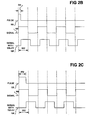
- FIGs. 2A, 2B, and 2C are timing diagrams showing examples of how different lengths of the pulse 108 affect the phase delay introduced into the first signal 106, according to varying embodiments of the invention, so that the signal 106 becomes synchronized with the second signal 112, as the modified first signal 106'.
- the length 350 of the pulse 108 is one-half of the clock cycle length 352. This introduces a 180-degree phase delay into the signal 106, such that the modified signal 106' is 180 degrees out of phase as compared to the signal 106.
- the length 354 of the pulse 108 is one-quarter of the clock cycle length 352, introducing a 90-degree phase delay into the signal 106, such that the modified signal 106' is 90 degrees out of phase relative to the signal 106.
- the length 356 of the pulse 108 is three-quarters of the clock cycle length 352, introducing a 270-degree phase delay into the signal 106, resulting in the modified signal 106' being 270 degrees out of phase relative to the signal 106.
- the proportion of the length of the pulse 108 relative to the clock cycle length 352 is the proportion of 360 degrees by which the signal 106 will be delayed, resulting in the modified signal 106'. That is, the length of the pulse 108, divided by the length of the clock cycle 352, times 360 degrees is the of phase delay that is introduced into the signal 106, in one embodiment of the invention.
- the clock cycle length 352 may be twelve nanoseconds.
- the difference in phase between the first signal 106 and the second signal 112 may be six nanoseconds. Therefore, the pulse 108 is six nanoseconds in length, and the signal 106 is delayed by 180 degrees, or six nanoseconds in this example, becoming the modified signal 106', and corresponding to the timing diagram of FIG. 2A.
- the pulse 108 is three nanoseconds, representing a difference in phase between the signals 106 and 112 of three nanoseconds
- the signal 106 is delayed by 90 degrees, or three nanoseconds in this example, becoming the modified signal 106', and corresponding to the timing diagram of FIG. 2B.
- the pulse 108 is nine nanoseconds, representing a phase difference between the signals 106 and 112 of nine nanoseconds
- the signal 106 is delayed by 270 degrees, or nine nanoseconds in this example, becoming the modified signal 106', and corresponding to the timing diagram of FIG. 2C.
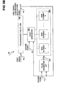
- FIGs. 3A and 3B show differing embodiments for implementing the mechanism 104.
- the mechanism 104 includes a delay line 206, a number of output elements 204A, 204B, ..., 204N, a logic mechanism 202, and a programmable delay line 208.
- the mechanism 104 also includes the pulse generator 110, as before.
- Each of the components of FIG. 3A can be considered as the means for performing its respective functionality.
- the pulse generator 110 in the embodiment of FIG. 3A specifically determines the phase difference between the second signal 112 and the output of the programmable delay line 208, which ultimately becomes the modified first signal 106', representing the first signal 106 as synchronized with the second signal 112. That is, the mechanism 104 utilizes feedback such that the modified first signal 106' is an input to the pulse generator 110.
- the modified first signal 106' is initially the first signal 106, such that the pulse 108 represents the phase difference between the first signal 106 and the second signal 112.
- the pulse generator 110 effectively receives as inputs both the first signal 106 and the second signal 112 in this embodiment.
- the pulse 108 is a flat line, such that there is no pulse in actuality.
- the output elements 204A, 204B, ..., 204N are collectively referred to as the output elements 204.
- the delay line 206 sets at least some of the output elements 204 based on the pulse 108 generated by the pulse generator 110.
- the delay line 206 thus effectively measures the length of the pulse 108, where the length of the pulse 108 is proportional to the phase difference between the signals 106 and 112.
- the delay line 206 sets at least some of the output elements 204 in proportional correspondence with the length of the pulse 108.
- the logic mechanism 202 may be implemented as hardware, software, or a combination of hardware and software, as can be appreciated by those of ordinary skill within the art.
- the logic mechanism 202 counts the number of the output elements 204 that have been set by the delay line 206.
- the logic mechanism 202 programs the programmable delay line 208 based on this counting.
- the signal 106 is delayed by the phase difference between the first signal 106 and the second signal 112, resulting in the modified signal 106'.
- the programmable delay line 208 may also be implemented as hardware, software, or a combination of hardware and software, as can be appreciated by those of ordinary skill within the art.
- the logic mechanism 202 in one embodiment also has inputs thereto including the second signal 112 and the modified first signal 106'. This is to determine the phase of the first signal 106 relative to the second signal 112, so that it can be determined whether the phase difference between the first signal 106 and the second signal 112 is to be added to or subtracted from the first signal 106 so that the two signals 106 and 112 become synchronized.
- the modified first signal 106' being input to the logic mechanism 202 thus represents another instance of feedback within the mechanism 104, as is the case with the modified first signal 106' relative to the pulse generator 110.
- the subtraction of the phase difference from the first signal 106 may occur due to a nominal delay being present in the delay line 208.
- the subtraction of addition of the phase diffe rence thus occurs relative to this delay.
- the nominal delay may be an integer number of cycles of the first signal 106, such that when the modified first signal 106' is compared to the second signal 112, the correct phase difference results.
- the mechanism 202 determines in this embodiment whether this difference is to be added to or subtracted from the first signal 106 in yielding the modified first signal 106' that is synchronized with the second signal 112. As is the case with the pulse generator 110, the logic mechanism 202 in actuality receives the modified first signal 106' as an input. The modified first signal 106' is initially the first signal 106 until it becomes synchronized with the second signal 112. Thus, the logic mechanism 202 effectively receives as inputs both the first signal 106 and the second signal 112 in this embodiment.
- the length of the pulse 108 is a fraction of the clock cycle length 352 of FIGs. 2A2C, where the clock cycle length 352 may be twelve nanoseconds in length. If the pulse 108 has a length of six nanoseconds, representing a phase difference between the signals 106 and 112 of six nanoseconds, then the delay line 206 sets six of the output elements 204, which are counted by the logic mechanism 202 to program the programmable delay line 208 to delay the signal 106 by six nanoseconds, or 180 degrees, in the signal 106 becoming the modified signal 106'. That is, the proportion of the length of the pulse 108 to the clock cycle length 352 is the proportion of the output elements 204 that the delay line 206 sets, and which the logic mechanism 202 counts to correspondingly program the programmable delay line 208.
- the mechanism 104 of the embodiment of FIG. 3A is non-iterative.
- the pulse 108 results in the delay line 206 setting at least some of the output elements 204, which are counted by the logic mechanism 202 to program the programmable delay line 208.
- the logic mechanism 202 thus programs the programmable delay line 208 with the delay to be introduced into the signal 106, either by addition or subtraction, as has been described.
- the signal 106 passes th rough the programmable delay line 208, the resulting signal 106' is synchronized with the signal 112. No further modification of the delay of the signal 106' is needed to achieve synchronization. That is, no iterative actions are taken to synchronize the signal 106, as the resulting signal 106', with the signal 112.
- the mechanism 104 includes elements 302, including the elements 303A, 303B, ..., 302N, as well as the logic mechanism 202 and the programmable delay line 208.
- the mechanism 104 also includes the pulse generator 110, as before.
- the mechanism 104 utilizes feedback such that the modified first signal 106' is an input to the pulse generator 110, in addition to the second signal 112 being an input.
- each of the components of FIG. 3B can be considered the means for performing its respective functionality.
- a number of the elements 302 are set based on the pulse 108. That is, a number of the elements 302 are set in proportional correspondence to the length of the pulse 108, where the length of the pulse 108 is proportional to the phase difference between the signals 106 and 112.
- the logic mechanism 202 then counts the number of the elements 302 that have been set, and correspondingly programs the progra mmable delay line 208 based on this counting. By passing through the programmable delay line 208 as has been programmed, the signal 106 becomes synchronized with the signal 112, as the modified signal 106'.
- the logic mechanism 202 of the embodiment of FIG. 3B may have inputs thereto including the second signal 112 and the modified signal 106, to determine the phase of the first signal 106 relative to the second signal 112.
- the logic mechanism 202 in this embodiment is able to determine whether the phase difference between the signals 106 and 112 is to be added to or subtracted from the first signal 106, so that the signals 106 and 112 become synchronized.
- the modified first signal 106' being input to the logic mechanism 202 thus represents another instance of feedback within the mechanism 104, as is the case with the modified first signal 106' relative to the pulse generator 110.
- the length of the pulse 108 is a fraction of the clock cycle length 352 of FIGs. 2A-2C, where the clock cycle length 352 may be twelve nanoseconds in length. If the pulse 108 is four nanoseconds in length, representing a phase difference between the signals 106 and 112 of four nanoseconds, then three of the elements 302 are set. These elements are counted by the logic mechanism 202 to program the programmable delay line 208 to delay the signal 106 by four nanoseconds, or 120 degrees, in the signal 106 becoming the modified signal 106' that is synchronized with the signal 112.
- the proportion of the length of the pulse 108 to the clock cycle 352 is the proportion of the elements 302 that the pulse 108 sets, and which the logic mechanism 202 counts to correspondingly program the programmable delay line 208.
- the mechanism 104 of the embodiment of FIG. 3B is non-iterative.
- the pulse 108 sets at least some of the elements 302, which are counted by the logic mechanism 202 to program the programmable delay line 208.
- the logic mechanism 202 thus programs the programmable delay line 208 with the desired phase delay to be introduced into the signal 106, either by addition or subtraction, as has been described.
- the resulting signal 106' is synchronized with the signal 112. No further delay of the signal 106' is needed to achieve synchronization. That is, no iterative actions are taken to synchronize the signal 106, as the signal 106', with the signal 112.
- FIG. 4 shows a more detailed implementation of the mechanism 104, according to an embodiment of the invention.
- the mechanism 104 of the embodiment of FIG. 4 is consistent with the mechanism 104 of each of the embodiments of FIGs. 3A and 3B.
- the mechanism 104 of the embodiment of FIG. 4 includes a number of delay elements 402A, 402B, ..., 402N, collectively referred to as the delay elements 402, a number of AND gates 404A, 404B, ..., 404N, collectively referred to as the AND gates 404, and a number of flip-flops 406A, 406B, ... 406N, collectively referred to as the flip-flops 406.
- the mechanism 104 also includes the pulse generator 110, the logic mechanism 202, and the programmable delay line 208.
- each of the components of FIG. 4 can be considered the means for performing its respective functionality.
- the delay line 206 of FIG. 3A can be considered in one embodiment to include the delay elements 402, as shown in FIG. 4, and the output elements 204 of FIG. 3A can be considered to include the flip-flops 406 and/or the AND gates 404.
- the elements 302 of FIG. 3B can be considered in one embodiment to include the delay elements 402, the AND gates 404, and/or the flip-flops 406, as is shown in FIG. 4.
- the pulse generator 110 generates the pulse 108 based on the second signal 112 and effectively on the first signal 106, as the modified first signal 106'.
- the pulse 108 propagates through the delay elements 402.
- Each of the delay elements 402 delays the pulse 108 from reaching a successive one of the delay elements 402 by a predetermined length of time.
- the delay elements 402 are combinatorial logic devices, or are analog devices.
- the output of each of the delay elements 402, as well as the pulse 108, serve as the inputs to the AND gates 404.
- Each of the AND gates 404 thus output a logic one only when both of its inputs are high. For example, if the pulse 108 has a length of five nanoseconds, and each of the delay elements 402 represents a delay of one nanosecond, five of the AND gates 404 will output logic ones.
- the reset line 408 is asserted and then deasserted prior to the pulse 108 being asserted, such as by the provider 102 of FIG. 1.
- the reset line 408 asynchronously resets the flip-flops 406 so that their outputs 412, which encompass the outputs 412A, 412B, ..., 412N, are logic zeros unless changed.
- Logic ones are asserted on the inputs 410, which encompass the inputs 410A, 410B, ..., 410N, of the flip-flops 406.
- the outputs 412 correspondingly switch to logic ones. If the clock inputs 414 do not transition from low to high, however, the outputs 412 of the flip-flops 406 remain at logic zeros.
- the outputs of the AND gates 404 in effect latch their corresponding flip-flops 406 when they transition from low to high.
- the logic mechanism 202 is then able to count the number of the flip-flops 406 that are outputting logic ones on their outputs 412. In response to this counting, the logic mechanism 202 correspondingly programs the programmable delay line 208, via the programming line 528. That is, the mechanism 202 programs the programmable delay line 208 based on the number of the flip-flops 406 that it has counted as outputting logic ones on their outputs 412, to synchronize the first signal 106 with the second signal 112. A greater or a lesser number of flip-flops 406 outputting logic ones results in the logic mechanism 202 programming the programmable delay line 208 with a greater or a lesser delay, respectively.
- the direction of the delay is based on a comparison of the phase of the second signal 112 and the first signal 106 as modified as the modified first signal 106'. This introduces a corresponding phase delay into the signal 106, resulting in modified first signal 106' being in phase with the second signal 112.
- An example is illustrative in describing operation of the mechanism 104 of the embodiment of FIG. 4.
- the clock cycle length may be ten nanoseconds
- the pulse 108 may be five nanoseconds in length
- each of the delay elements 402 may represent a one-nanosecond delay.
- the flip-flops 406 are reset via the reset line 408 before the pulse 108 is asserted.
- the first five of the delay elements 402 are able to propagate the pulse 108 such that the corresponding first five of the AND gates 404 have both their inputs high.
- the last five of the AND gates 404 during the five nanoseconds of the pulse 108 only one of each of their inputs is high, due to the pulse 108.
- the other input of each of these last five of the AND gates 404 remains low during these five nanoseconds, because the pulse 108 has not yet propagated through the corresponding last five of the delay elements 402. After the five nanoseconds of the pulse 108, one of each of their inputs will then be low, due to the pulse 108 having expired.
- the first five of the AND gates 404 transition the clock inputs 414 of the corresponding first five of the flip-flops 406 from low to high. These first five of the flip-flops 406 latch their corresponding outputs 412 at logic ones, and the outputs 412 of these first five of the flip-flops 406 remain at logic ones even after the first five of the AND gates 404 no longer assert their corresponding clock inputs 414. This enables the logic mechanism 202 to have sufficient time to count the number of the flip-flops 406 that have their outputs 412 at logic ones.
- the logic mechanism 202 thus counts five of the flip-flops 406 as outputting logic ones, and may correspondingly program either a positive or a negative five-nanosecond delay into the programmable delay line 208, depending on whether the phase of the modified first signal 106' is before or after that of the second signal 112.
- the delay line 208 then delays the first signal 106 by five nanoseconds, resulting in the modified signal 106' being in synchronization with the second signal 112.
- the flip-flops 406 are in one embodiment edge-triggered devices, meaning that they latch on the leading transition from low to high, or the lagging transition from high to low. However, in another embodiment, they may be level-triggered devices, meaning that they latch on a high input signal, and not on the transition from high to low or from low to high. Other types of devices are also amenable to embodiments of the invention.
- FIGs. 5A and 5B show embodiments of the pulse generator 110 and of the logic mechanism 202, respectively, that can be used in conjunction with the mechanism 104 of the embodiments of FIGs. 3A, 3B, and/or 4.
- the pulse generator 110 includes AND gates 504 and 508, and an exclusive-or (XOR) gate 506.
- the inputs to the AND gate 504 include an update line 502 and the second signal 112, whereas the inputs to the XOR gate 506 include the second signal 112 and the modified first signal 106'.
- the update line 502 is asserted high when then first signal 106 is desired to be synchronized with the second signal 112 as the first signal 106', and is asserted high until the first signal 106 has been synchronized with the second signal 112, usually within one clock cycle.
- the AND gate 504 serves to output a logic one when both the second signal 112 is asserting high, and the update line 502 has been asserted high.
- the XOR gate 506 actually generates the pulse that ultimately becomes the pulse 108. It accomplishes this by performing an XOR operation on the second signal 112 and the modified first signal 106'. When the second signal 112 and the modified first signal 106' are out of synch, such that one of the signals 112 and 106' is high and the other of the signals is low, the XOR gate 506 outputs a logic one. When both the second signal 112 and the modified first signal 106' are either low or high, the XOR gate 506 outputs a logic zero.
- the XOR gate 506 outputs a logic zero.
- the pulse specifically output by the XOR gate 506 is indicative of, and preferably proportional to, the amount of phase delay that is to be added to or subtracted from the first signal 106 to become synchronized with the second signal 112.
- the AND gate 508 acts to output the pulse generated by the XOR gate 506 as the pulse 108 when the AND gate 504 has output a logic one.
- the input to the AND gate 508 is replaced by just the update line 502, such that the AND gate 504 is not present. This effectively performs the same functionality as the pulse generator 110 of the embodiment shown in FIG. 5A.
- the pulse generator 110 can be just the XOR gate 506, having as inputs the second signal 112 and the modified signal 106', and having its output serve as the pulse 108.
- the update line 502 is not present, such that the first signal 106 is constantly modified to be synchronized with the second signal 112.
- the logic mechanism 202 includes an adder 520, an accumulator 522, and a phase detector 524. Each of these components may be considered the means for performing its respective functionality.
- the adder 520 counts, or adds together, the number of the outputs 412 of the flip-flops 406 of FIG. 4 that have been latched high, or at logic ones. In response, the adder 520 sets a number of bits of the accumulator 522 as the binary equivalent of the number of the outputs 412 that have been latched high.
- the adder 520 sets these bits of the accumulator 522 at 0x101, which is the binary equivalent of five.
- the phase detector 524 is in one embodiment a one-bit phase detector.
- the phase detector 524 detects whether the phase of the modified first signal 106' is ahead of or behind the phase of the second signal 112.
- the phase detector 524 may output the results of its comparison when the update line 502 is asserted high. That is, the phase detector 524 is operational when the update line 502 is asserted high.
- the phase detector 524 outputs a logic one bit when the modified first signal 106' has a phase ahead of the phase of the second signal 112, and outputs a logic zero when the phase of the signal 106' is behind the phase of the signal 112.
- This bit serves as the sign, or direction or carrier, bit 526 for the accumulator 522.
- the bit is set to logic zero, this means that the accumulator 522 is indicating on the line 528 that the magnitude of the accumulator 522 set by the adder 520 is to be added to the first signal 106 to yield the modified first signal 106'.
- the programming line 528 is set to 0x1101 to indicate subtraction, and 0x0101 to indicate addition, where the leading bit is the sign, or direction or carrier, bit 526.
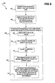
- FIG. 6 shows a method 600 according to an embodiment of the invention.
- the method 600 may be performed at least in part by the system 100 of FIG. 1 and/or the mechanism 104 of FIGs. 3A, 3B, and/or 4.
- a reset line and an update line are asserted, and then optionally deasserted, as necessary (602), such as the reset line 408 of FIG. 4 and the update line 502 of FIGs. 5A and 5B.
- a pulse is asserted, where the pulse is indicative of phase difference between a first signal and a second signal (604).
- the pulse may be the pulse 108 of FIGs. 1, 2A-2C, 3A-3B, 4, 5A, and/or 5B.
- the pulse may be generated, such as by the pulse generator 110 of FIGs.
- the first signal may be the first signal 106
- the second signal may be the second signal 112, of FIGs. 1, 2A-2C, 3A-3B, 4, 5A, and/or 5B.
- a phase delay is introduced into the first signal, based on the asserted pulse, to synchronize the first signal with the second signal (606).
- the phase delay may be subtracted from or added to the first signal to synchronize the first signal with the second signal.
- the length of the pulse is measured (608).
- the length of the pulse may be measured, for instance, by the delay line 206 of FIG. 3A.
- Elements are then set based on the length of the pulse as measured (610). These elements may be the output elements 204 of FIG. 3A, the elements 302 of FIG. 3B, and/or the flip-flops 406 of FIG. 4.
- the elements that have been set are counted (612), such as by the logic mechanism 202 of FIGS. 1, 3A-3B, 4, and/or 5B.
- the phase of the first signal relative to the phase of the second signal is determined (613), to determine whether the phase delay should be added to or subtracted from the first signal. This determination can be accomplished by the phase detector 524 of FIG. 5B. Finally, a programmable delay line is programmed based on the elements that have been set as counted (614), such as the programmable delay line 208 of FIGs. 1, 3A-3B, and/or 4. The first signal is thus synchronized with the second signal.
Landscapes
- Physics & Mathematics (AREA)
- Nonlinear Science (AREA)
- Engineering & Computer Science (AREA)
- Computer Networks & Wireless Communication (AREA)
- Signal Processing (AREA)
- Pulse Circuits (AREA)
- Indexing, Searching, Synchronizing, And The Amount Of Synchronization Travel Of Record Carriers (AREA)
- Manipulation Of Pulses (AREA)
- Magnetic Resonance Imaging Apparatus (AREA)
- Measuring Phase Differences (AREA)
Abstract
Description
Claims (10)
- A system (100) comprising:a provider (102) of a first signal and a second signal; and,a mechanism (104) to non-iteratively synchronize the first signal with the second signal based on a pulse indicative of a phase difference between the first signal and the second signal.
- The system of claim 1, wherein the mechanism comprises:a plurality of output elements (204);a delay line (206) to set a number of the plurality of output elements based on the pulse indicative of the phase difference between the first signal and the second signal;a logic mechanism (202) to count the number of the plurality of output elements set by the delay line; and,a programmable delay line (208) programmed by the logic mechanism based on the number of the plurality of output elements counted to synchronize the first signal with the second signal.
- The system of claim 2, wherein the mechanism further comprises a pulse mechanism (110) to generate the pulse indicative of the difference between the first signal and the second signal.
- The system of claim 2, wherein the delay line comprises a plurality of delay elements (402) corresponding to the plurality of output elements to measure the pulse, a number of which correspondingly set the number of the plurality of output elements based on a length of the pulse as being proportional to the phase difference between the first signal and the second signal.
- The system of claim 2, wherein the logic mechanism comprises:a phase detector (524) to determine a phase of the first signal relative to a phase of the second signal;an adder (520) to count the number of the plurality of output elements set by the delay line; and,an accumulator (522) to program the programmable delay line to synchronize the first signal with the second signal based on the phase determined by the phase detector and the number of the plurality of output elements counted by the adder.
- A circuit (104) to synchronize a first signal with a second signal comprising:a pulse mechanism (110) to generate a pulse indicative of a phase difference between the first signal and the second signal;a delay line (206) to measure a length of the pulse;a plurality of output elements (204), a number of which are set based on the length of the pulse measured;a logic mechanism (202) to count the number of the plurality of output elements set; and,a programmable delay line (208) programmed by the logic mechanism based on the number of the plurality of output elements counted to synchronize the first signal with the second signal.
- The circuit of claim 6, wherein the pulse mechanism comprises an XOR gate (506).
- The circuit of claim 6, wherein the delay line comprises a plurality of delay elements (402) corresponding to the plurality of output elements, a number of which correspondingly set the number of the plurality of output elements based on the length of the pulse measured as being proportional to the phase difference between the first signal and the second signal.
- The circuit of claim 6, wherein the plurality of output elements comprises a plurality of flip-flops (406).
- The circuit of claim 6, wherein the logic mechanism comprises:a phase detector (524) to determine a phase of the first signal relative to a phase of the second signal;an adder (520) to count the number of the plurality of output elements set by the delay line; and,an accumulator (522) to program the programmable delay line to synchronize the first signal with the second signal based on the phase determined by the phase detector and the number of the plurality of output elements counted by the adder.
Applications Claiming Priority (2)
| Application Number | Priority Date | Filing Date | Title |
|---|---|---|---|
| US262791 | 2002-10-02 | ||
| US10/262,791 US6885228B2 (en) | 2002-10-02 | 2002-10-02 | Non-iterative signal synchronization |
Publications (2)
| Publication Number | Publication Date |
|---|---|
| EP1406409A2 true EP1406409A2 (en) | 2004-04-07 |
| EP1406409A3 EP1406409A3 (en) | 2005-07-20 |
Family
ID=31993553
Family Applications (1)
| Application Number | Title | Priority Date | Filing Date |
|---|---|---|---|
| EP03009063A Withdrawn EP1406409A3 (en) | 2002-10-02 | 2003-04-17 | Non-iterative signal synchronization |
Country Status (2)
| Country | Link |
|---|---|
| US (1) | US6885228B2 (en) |
| EP (1) | EP1406409A3 (en) |
Families Citing this family (3)
| Publication number | Priority date | Publication date | Assignee | Title |
|---|---|---|---|---|
| KR100731449B1 (en) | 2005-09-13 | 2007-06-21 | 세이코 엡슨 가부시키가이샤 | Pulse generator circuit and electronic device using this circuit, mobile phone, personal computer, and information transmission method using this circuit |
| US7973549B2 (en) * | 2007-06-12 | 2011-07-05 | International Business Machines Corporation | Method and apparatus for calibrating internal pulses in an integrated circuit |
| TWI448075B (en) * | 2008-09-12 | 2014-08-01 | Foxnum Technology Co Ltd | Pulse generate device |
Family Cites Families (28)
| Publication number | Priority date | Publication date | Assignee | Title |
|---|---|---|---|---|
| SE449544B (en) | 1985-09-06 | 1987-05-04 | Ellemtel Utvecklings Ab | FASAVSTEMNINGSANORDNING |
| US4795985A (en) * | 1986-04-01 | 1989-01-03 | Hewlett-Packard Company | Digital phase lock loop |
| US5212716A (en) | 1991-02-05 | 1993-05-18 | International Business Machines Corporation | Data edge phase sorting circuits |
| US5477330A (en) | 1992-10-16 | 1995-12-19 | Printware, Inc. | Synchronization to a start-of-scan detection, and digital generation of variable frequencies, from a fixed-frequency fixed-phase frequency source in an image generator in order to highly accurately time the placement of pixels upon a scan line |
| US5438353A (en) | 1992-11-02 | 1995-08-01 | Hewlett-Packard Company | Clock signal generator for electrophotographic printers |
| US5463337A (en) | 1993-11-30 | 1995-10-31 | At&T Corp. | Delay locked loop based clock synthesizer using a dynamically adjustable number of delay elements therein |
| US5760816A (en) | 1996-02-06 | 1998-06-02 | Hewlett-Packard Company | Variable phase clock generator for an electrophotographic printer |
| US5793709A (en) | 1996-04-19 | 1998-08-11 | Xli Corporation | Free loop interval timer and modulator |
| JP3487532B2 (en) * | 1996-07-08 | 2004-01-19 | 株式会社東芝 | Data processing device, semiconductor storage device, and data processing method |
| US5940608A (en) | 1997-02-11 | 1999-08-17 | Micron Technology, Inc. | Method and apparatus for generating an internal clock signal that is synchronized to an external clock signal |
| US5945862A (en) | 1997-07-31 | 1999-08-31 | Rambus Incorporated | Circuitry for the delay adjustment of a clock signal |
| US6052011A (en) | 1997-11-10 | 2000-04-18 | Tritech Microelectronics, Ltd. | Fractional period delay circuit |
| US5990923A (en) | 1997-11-14 | 1999-11-23 | Hewlett-Packard Company | High resolution dynamic pulse width modulation |
| KR100261216B1 (en) | 1997-11-21 | 2000-07-01 | 윤종용 | Programmable delay line |
| US6289068B1 (en) | 1998-06-22 | 2001-09-11 | Xilinx, Inc. | Delay lock loop with clock phase shifter |
| EP1040578A1 (en) | 1998-08-04 | 2000-10-04 | Koninklijke Philips Electronics N.V. | A delay locked loop with harmonic lock detection |
| US6300807B1 (en) * | 1998-09-04 | 2001-10-09 | Hitachi, Ltd. | Timing-control circuit device and clock distribution system |
| JP3344466B2 (en) * | 1998-11-04 | 2002-11-11 | 日本電気株式会社 | Signal transfer control method and circuit thereof |
| KR100295056B1 (en) | 1999-01-27 | 2001-07-12 | 윤종용 | Loop &method for delay-locking |
| US6259467B1 (en) | 1999-02-09 | 2001-07-10 | International Business Machines Corporation | Multi stage oscillator phase alignment scheme |
| JP3630291B2 (en) * | 1999-03-01 | 2005-03-16 | シャープ株式会社 | Timing generator |
| US6390579B1 (en) | 1999-04-15 | 2002-05-21 | Hewlett-Packard Company | Pulse width modulator using delay-line technology with automatic calibration of delays to desired operating frequency |
| US6236427B1 (en) | 1999-04-15 | 2001-05-22 | Hewlett-Packard Company | Edge placement device |
| US20010013802A1 (en) * | 1999-07-07 | 2001-08-16 | Ghene Faulcon | System and process for high speed interface clock skew correction |
| US6366307B1 (en) | 2000-03-24 | 2002-04-02 | Hewlett-Packard Co. | Clock independent pulse width modulation |
| US6340986B1 (en) | 2000-03-24 | 2002-01-22 | Hewlett-Packard Company | Method and device for time shifting transitions in an imaging device |
| US6335751B1 (en) | 2000-03-24 | 2002-01-01 | Hewlett-Packard Co. | System and method for rendering an output image onto an image transfer surface using multiple optical scan paths |
| US6917228B2 (en) * | 2002-06-06 | 2005-07-12 | Micron Technology, Inc. | Delay locked loop circuit with time delay quantifier and control |
-
2002
- 2002-10-02 US US10/262,791 patent/US6885228B2/en not_active Expired - Fee Related
-
2003
- 2003-04-17 EP EP03009063A patent/EP1406409A3/en not_active Withdrawn
Also Published As
| Publication number | Publication date |
|---|---|
| US20040066221A1 (en) | 2004-04-08 |
| US6885228B2 (en) | 2005-04-26 |
| EP1406409A3 (en) | 2005-07-20 |
Similar Documents
| Publication | Publication Date | Title |
|---|---|---|
| US8416001B2 (en) | Techniques for reducing duty cycle distortion in periodic signals | |
| CN113711510B (en) | Phase predictor and associated method of use | |
| US8422619B2 (en) | Clock frequency divider circuit, clock distribution circuit, clock frequency division method, and clock distribution method | |
| US6917660B2 (en) | Adaptive de-skew clock generation | |
| US7042250B1 (en) | Synchronization of clock signals in a multi-clock domain | |
| US6960942B2 (en) | High speed phase selector | |
| JP4944894B2 (en) | Method and apparatus for adjusting a synchronous clock signal | |
| EP1406409A2 (en) | Non-iterative signal synchronization | |
| US10177747B2 (en) | High resolution capture | |
| TWI778557B (en) | True random number generator and true random number generating method | |
| KR101639064B1 (en) | Heterogeneous sampling delay-line time-to-digital converter | |
| US7684533B2 (en) | Phase lock loop jitter measurement | |
| US6980041B2 (en) | Non-iterative introduction of phase delay into signal without feedback | |
| JP2024022445A (en) | entropy source circuit | |
| KR20200106735A (en) | Shift register | |
| US11239849B2 (en) | Locked loop circuit and method with multi-phase synchronization | |
| US10355691B2 (en) | Minimizing information leakage from combinatorial logic | |
| US6777993B1 (en) | Method and apparatus for adjusting the phase and frequency of a periodic wave | |
| US8270557B2 (en) | Integrated circuit and method for driving the same | |
| US20060269030A1 (en) | Phase lock loop jitter measurement | |
| KR20240035721A (en) | Measurement and control of clock signal phases | |
| Park et al. | Design and Analysis of Asynchronous Sampling Duty Cycle Corrector. Electronics 2021, 10, 2594 | |
| US20060250161A1 (en) | Fast linear phase detector | |
| KR0146976B1 (en) | Synchronous Up / Down Counter | |
| Chattopadhyay et al. | Design and operating characteristics of a reconfigurable clock distribution network |
Legal Events
| Date | Code | Title | Description |
|---|---|---|---|
| PUAI | Public reference made under article 153(3) epc to a published international application that has entered the european phase |
Free format text: ORIGINAL CODE: 0009012 |
|
| AK | Designated contracting states |
Kind code of ref document: A2 Designated state(s): AT BE BG CH CY CZ DE DK EE ES FI FR GB GR HU IE IT LI LU MC NL PT RO SE SI SK TR |
|
| AX | Request for extension of the european patent |
Extension state: AL LT LV MK |
|
| PUAL | Search report despatched |
Free format text: ORIGINAL CODE: 0009013 |
|
| AK | Designated contracting states |
Kind code of ref document: A3 Designated state(s): AT BE BG CH CY CZ DE DK EE ES FI FR GB GR HU IE IT LI LU MC NL PT RO SE SI SK TR |
|
| AX | Request for extension of the european patent |
Extension state: AL LT LV MK |
|
| RIC1 | Information provided on ipc code assigned before grant |
Ipc: 7H 04J 3/06 B Ipc: 7H 04L 7/02 A |
|
| AKX | Designation fees paid | ||
| STAA | Information on the status of an ep patent application or granted ep patent |
Free format text: STATUS: THE APPLICATION IS DEEMED TO BE WITHDRAWN |
|
| 18D | Application deemed to be withdrawn |
Effective date: 20060121 |
|
| REG | Reference to a national code |
Ref country code: DE Ref legal event code: 8566 |