EP1404507B1 - Oled film and method for its forming - Google Patents
Oled film and method for its forming Download PDFInfo
- Publication number
- EP1404507B1 EP1404507B1 EP02743307A EP02743307A EP1404507B1 EP 1404507 B1 EP1404507 B1 EP 1404507B1 EP 02743307 A EP02743307 A EP 02743307A EP 02743307 A EP02743307 A EP 02743307A EP 1404507 B1 EP1404507 B1 EP 1404507B1
- Authority
- EP
- European Patent Office
- Prior art keywords
- oled
- plane
- film
- substrate
- forming
- Prior art date
- Legal status (The legal status is an assumption and is not a legal conclusion. Google has not performed a legal analysis and makes no representation as to the accuracy of the status listed.)
- Expired - Lifetime
Links
- 238000000034 method Methods 0.000 title claims abstract description 29
- 239000000758 substrate Substances 0.000 claims abstract description 43
- 239000000463 material Substances 0.000 claims abstract description 17
- 239000004033 plastic Substances 0.000 claims abstract description 17
- 229920003023 plastic Polymers 0.000 claims abstract description 17
- 229920001940 conductive polymer Polymers 0.000 claims abstract description 14
- 239000011241 protective layer Substances 0.000 claims abstract description 7
- 230000006835 compression Effects 0.000 claims abstract description 6
- 238000007906 compression Methods 0.000 claims abstract description 6
- 238000005187 foaming Methods 0.000 claims 1
- 239000010410 layer Substances 0.000 description 63
- 229920000767 polyaniline Polymers 0.000 description 10
- 239000004020 conductor Substances 0.000 description 6
- 238000004519 manufacturing process Methods 0.000 description 6
- 238000005452 bending Methods 0.000 description 4
- 239000010931 gold Substances 0.000 description 4
- 229920000642 polymer Polymers 0.000 description 4
- 238000012360 testing method Methods 0.000 description 4
- 238000007666 vacuum forming Methods 0.000 description 4
- 239000011248 coating agent Substances 0.000 description 3
- 238000000576 coating method Methods 0.000 description 3
- 229910052737 gold Inorganic materials 0.000 description 3
- 229910052751 metal Inorganic materials 0.000 description 3
- 239000002184 metal Substances 0.000 description 3
- 229920000728 polyester Polymers 0.000 description 3
- 229910052709 silver Inorganic materials 0.000 description 3
- NIXOWILDQLNWCW-UHFFFAOYSA-M Acrylate Chemical compound [O-]C(=O)C=C NIXOWILDQLNWCW-UHFFFAOYSA-M 0.000 description 2
- 239000004743 Polypropylene Substances 0.000 description 2
- 229910052782 aluminium Inorganic materials 0.000 description 2
- 239000010949 copper Substances 0.000 description 2
- 238000001704 evaporation Methods 0.000 description 2
- 239000011521 glass Substances 0.000 description 2
- 239000011777 magnesium Substances 0.000 description 2
- 239000011159 matrix material Substances 0.000 description 2
- 238000005259 measurement Methods 0.000 description 2
- 239000004417 polycarbonate Substances 0.000 description 2
- 229920000515 polycarbonate Polymers 0.000 description 2
- -1 polyethylene terephthalate Polymers 0.000 description 2
- 229920000139 polyethylene terephthalate Polymers 0.000 description 2
- 239000005020 polyethylene terephthalate Substances 0.000 description 2
- 229920001155 polypropylene Polymers 0.000 description 2
- 239000005725 8-Hydroxyquinoline Substances 0.000 description 1
- RYGMFSIKBFXOCR-UHFFFAOYSA-N Copper Chemical compound [Cu] RYGMFSIKBFXOCR-UHFFFAOYSA-N 0.000 description 1
- WHXSMMKQMYFTQS-UHFFFAOYSA-N Lithium Chemical compound [Li] WHXSMMKQMYFTQS-UHFFFAOYSA-N 0.000 description 1
- FYYHWMGAXLPEAU-UHFFFAOYSA-N Magnesium Chemical compound [Mg] FYYHWMGAXLPEAU-UHFFFAOYSA-N 0.000 description 1
- 208000031481 Pathologic Constriction Diseases 0.000 description 1
- 229920000109 alkoxy-substituted poly(p-phenylene vinylene) Polymers 0.000 description 1
- 239000004411 aluminium Substances 0.000 description 1
- XAGFODPZIPBFFR-UHFFFAOYSA-N aluminium Chemical compound [Al] XAGFODPZIPBFFR-UHFFFAOYSA-N 0.000 description 1
- REDXJYDRNCIFBQ-UHFFFAOYSA-N aluminium(3+) Chemical compound [Al+3] REDXJYDRNCIFBQ-UHFFFAOYSA-N 0.000 description 1
- 239000010405 anode material Substances 0.000 description 1
- QVGXLLKOCUKJST-UHFFFAOYSA-N atomic oxygen Chemical compound [O] QVGXLLKOCUKJST-UHFFFAOYSA-N 0.000 description 1
- 150000001875 compounds Chemical class 0.000 description 1
- 229910052802 copper Inorganic materials 0.000 description 1
- 230000003247 decreasing effect Effects 0.000 description 1
- 230000000593 degrading effect Effects 0.000 description 1
- 238000013461 design Methods 0.000 description 1
- 230000000694 effects Effects 0.000 description 1
- 230000005611 electricity Effects 0.000 description 1
- 230000005670 electromagnetic radiation Effects 0.000 description 1
- 230000008020 evaporation Effects 0.000 description 1
- 230000005284 excitation Effects 0.000 description 1
- PCHJSUWPFVWCPO-UHFFFAOYSA-N gold Chemical compound [Au] PCHJSUWPFVWCPO-UHFFFAOYSA-N 0.000 description 1
- 238000010438 heat treatment Methods 0.000 description 1
- AMGQUBHHOARCQH-UHFFFAOYSA-N indium;oxotin Chemical compound [In].[Sn]=O AMGQUBHHOARCQH-UHFFFAOYSA-N 0.000 description 1
- 238000001746 injection moulding Methods 0.000 description 1
- 238000003780 insertion Methods 0.000 description 1
- 230000037431 insertion Effects 0.000 description 1
- 239000005001 laminate film Substances 0.000 description 1
- 229910052744 lithium Inorganic materials 0.000 description 1
- 229910052749 magnesium Inorganic materials 0.000 description 1
- 150000002739 metals Chemical class 0.000 description 1
- 238000012986 modification Methods 0.000 description 1
- 230000004048 modification Effects 0.000 description 1
- 238000004776 molecular orbital Methods 0.000 description 1
- 239000011368 organic material Substances 0.000 description 1
- 229910052760 oxygen Inorganic materials 0.000 description 1
- 239000001301 oxygen Substances 0.000 description 1
- 229960003540 oxyquinoline Drugs 0.000 description 1
- 238000004806 packaging method and process Methods 0.000 description 1
- 238000000059 patterning Methods 0.000 description 1
- 238000007639 printing Methods 0.000 description 1
- 230000001681 protective effect Effects 0.000 description 1
- MCJGNVYPOGVAJF-UHFFFAOYSA-N quinolin-8-ol Chemical compound C1=CN=C2C(O)=CC=CC2=C1 MCJGNVYPOGVAJF-UHFFFAOYSA-N 0.000 description 1
- 238000007789 sealing Methods 0.000 description 1
- 239000004332 silver Substances 0.000 description 1
- 238000007669 thermal treatment Methods 0.000 description 1
Images


Classifications
-
- B—PERFORMING OPERATIONS; TRANSPORTING
- B29—WORKING OF PLASTICS; WORKING OF SUBSTANCES IN A PLASTIC STATE IN GENERAL
- B29C—SHAPING OR JOINING OF PLASTICS; SHAPING OF MATERIAL IN A PLASTIC STATE, NOT OTHERWISE PROVIDED FOR; AFTER-TREATMENT OF THE SHAPED PRODUCTS, e.g. REPAIRING
- B29C51/00—Shaping by thermoforming, i.e. shaping sheets or sheet like preforms after heating, e.g. shaping sheets in matched moulds or by deep-drawing; Apparatus therefor
- B29C51/10—Forming by pressure difference, e.g. vacuum
-
- H—ELECTRICITY
- H05—ELECTRIC TECHNIQUES NOT OTHERWISE PROVIDED FOR
- H05B—ELECTRIC HEATING; ELECTRIC LIGHT SOURCES NOT OTHERWISE PROVIDED FOR; CIRCUIT ARRANGEMENTS FOR ELECTRIC LIGHT SOURCES, IN GENERAL
- H05B33/00—Electroluminescent light sources
- H05B33/10—Apparatus or processes specially adapted to the manufacture of electroluminescent light sources
-
- H—ELECTRICITY
- H10—SEMICONDUCTOR DEVICES; ELECTRIC SOLID-STATE DEVICES NOT OTHERWISE PROVIDED FOR
- H10K—ORGANIC ELECTRIC SOLID-STATE DEVICES
- H10K71/00—Manufacture or treatment specially adapted for the organic devices covered by this subclass
-
- B—PERFORMING OPERATIONS; TRANSPORTING
- B29—WORKING OF PLASTICS; WORKING OF SUBSTANCES IN A PLASTIC STATE IN GENERAL
- B29C—SHAPING OR JOINING OF PLASTICS; SHAPING OF MATERIAL IN A PLASTIC STATE, NOT OTHERWISE PROVIDED FOR; AFTER-TREATMENT OF THE SHAPED PRODUCTS, e.g. REPAIRING
- B29C2791/00—Shaping characteristics in general
- B29C2791/004—Shaping under special conditions
- B29C2791/006—Using vacuum
-
- B—PERFORMING OPERATIONS; TRANSPORTING
- B29—WORKING OF PLASTICS; WORKING OF SUBSTANCES IN A PLASTIC STATE IN GENERAL
- B29C—SHAPING OR JOINING OF PLASTICS; SHAPING OF MATERIAL IN A PLASTIC STATE, NOT OTHERWISE PROVIDED FOR; AFTER-TREATMENT OF THE SHAPED PRODUCTS, e.g. REPAIRING
- B29C2791/00—Shaping characteristics in general
- B29C2791/004—Shaping under special conditions
- B29C2791/007—Using fluid under pressure
-
- B—PERFORMING OPERATIONS; TRANSPORTING
- B29—WORKING OF PLASTICS; WORKING OF SUBSTANCES IN A PLASTIC STATE IN GENERAL
- B29C—SHAPING OR JOINING OF PLASTICS; SHAPING OF MATERIAL IN A PLASTIC STATE, NOT OTHERWISE PROVIDED FOR; AFTER-TREATMENT OF THE SHAPED PRODUCTS, e.g. REPAIRING
- B29C51/00—Shaping by thermoforming, i.e. shaping sheets or sheet like preforms after heating, e.g. shaping sheets in matched moulds or by deep-drawing; Apparatus therefor
-
- B—PERFORMING OPERATIONS; TRANSPORTING
- B29—WORKING OF PLASTICS; WORKING OF SUBSTANCES IN A PLASTIC STATE IN GENERAL
- B29L—INDEXING SCHEME ASSOCIATED WITH SUBCLASS B29C, RELATING TO PARTICULAR ARTICLES
- B29L2031/00—Other particular articles
- B29L2031/30—Vehicles, e.g. ships or aircraft, or body parts thereof
- B29L2031/3055—Cars
- B29L2031/3061—Number plates
-
- B—PERFORMING OPERATIONS; TRANSPORTING
- B29—WORKING OF PLASTICS; WORKING OF SUBSTANCES IN A PLASTIC STATE IN GENERAL
- B29L—INDEXING SCHEME ASSOCIATED WITH SUBCLASS B29C, RELATING TO PARTICULAR ARTICLES
- B29L2031/00—Other particular articles
- B29L2031/34—Electrical apparatus, e.g. sparking plugs or parts thereof
- B29L2031/3431—Telephones, Earphones
-
- H—ELECTRICITY
- H10—SEMICONDUCTOR DEVICES; ELECTRIC SOLID-STATE DEVICES NOT OTHERWISE PROVIDED FOR
- H10K—ORGANIC ELECTRIC SOLID-STATE DEVICES
- H10K71/00—Manufacture or treatment specially adapted for the organic devices covered by this subclass
- H10K71/40—Thermal treatment, e.g. annealing in the presence of a solvent vapour
Definitions
- the object of the present invention is an OLED film according to the preamble of Claim 1.
- the object of the present invention is also a method for forming an OLED film according to the preamble of Claim 4.
- OLED organic light emitting diode structures
- An OLED film is usually formed by evaporating OLED layers onto a substrate.
- OLED layers typically comprise a first electrode, a layer of emitting material and a second electrode as well as intermediate and protective layers.
- OILED layers may be formed so that they cover the whole substrate, or so that they will form several different OLED components or OLED areas on the substrate.
- OLED structures From layer-structured OLED structures, one may form large consistent plane surfaces which endure bending so that they can be formed into evenly curved surfaces. Thus, from a plane OLED structure, one is able to form, for example, a curved surface which follows the cylindrical surface below it. The OLED structure deflects thus only to the direction of the cylindrical surface perimeter, whereas the material structure of electrodes in the OLED structure remains unbroken. Then the electrical conductivity of electrodes in the direction of the plane surface is maintained. Such structures may be used in, for example, background lighting.
- the FI patent application 981731 presents an OLED structure in which the light emitting layer between the electrodes is sol gel glass, into which one has chemically inserted material with an effect on the opto-electric characteristics.
- the EP patent publication 1065737 presents an OLED structure in which an electron hole injecting layer has been placed between the anode and the light emitting layer. On the other hand, an electron-emitting layer has been placed between the cathode and the light emitting material.
- the US patent 5,970,318 presents a structure which endures mechanical bending and consists of an OLED and a transistor, and which may be used in flexible displays.
- This OLED comprises a transparent electrode formed on a substrate, an organic light emitting layer formed on the electrode, and an upper electrode formed on the emitting layer.
- the US patent 6,046,543 presents a reversed OLED structure.
- This structure comprises a substrate, a polymer layer on top of the substrate, a cathode on top of the polymer layer, an electron transporting layer on top of the cathode, a light emitting layer on top of the electron transporting layer, a hole transporting layer on top of the light emitting layer, a protective layer on top of the hole transporting layer, and an anode on top of the protective layer.
- a layer-structured OLED structure does not remain unbroken and functional if a plane OLED structure is bent in the direction of several axes pointing to different directions in the plane surface.
- one has not been able to form areas ascended from the level surface into the plane OLED surface, for instance hemispherical areas. This matter has limited the use of the OLED structure in applications in which one could use plane surfaces, and such plane surfaces which curve in the direction of the perimeter of cylindrical surface.
- OLED structures were not usable in such objects in which the OLED structure should be formed on a surface bending in the direction of several axes, such as on hemisphere.
- an OLED area ascended from a plane OLED surface could be constructed directly by coating OLED layers on a non-flat surface, for example on a hemisphere, but this option is not practical or productive. Then, the non-flat surface which is coated by evaporation should be rotated during coating. In addition, it is difficult to form an even coating on a non-flat rotating surface.
- ascended OLED areas may be formed on a plane OLED structure so that the functionality of the OLED structure is maintained.
- pieces of desired shape may be cut from a plane OLED structure so that the functionality of the OLED structure is maintained.
- an ascended area or ascended areas may be formed on a plane OLED film, which comprises a substrate and OLED layers formed on it.
- This structure is produced by forming an OLED known per se, which endures forming, temperature loading and mechanical stress, with forming methods known per se which are suited for forming plastic-like materials, such as vacuum forming, pressure forming, matched-mould forming or their combination in a plastic forming machine.
- OLED film thus produced, one is able to, for example, generate light on a surface of desired shape or use the produced structure for patterning purposes.
- One may thus utilise an unused non-flat surface or space in, for instance, portable electronics products.
- Other possible applications for structures according to the invention are, for example, integrated background lights in different consumer goods, such as watches.
- the forming may be done so that only the OLED film is formed, after which the formed OLED film is inserted as a part of the product in which one wishes to utilise the light generated by the OLED component.
- the forming may also be done so that the OLED film is formed together with the product the part of which one wishes the OLED film to become. This could be, for instance, a situation in which one wishes the OLED film to be a part of a plastic piece. Then the OLED film is combined to a plastic blank and both parts are formed together in a plastic forming process.
- the plane OLED film is placed over a mould and fastened from its edges to the mould. After this, vacuum is produced to the space between the mould and OLED film, whereas the OLED film sticks onto the surfaces of the mould. Thus, the OLED film is formed to the shape defined by the mould surfaces.
- the plane OLED film is placed over a mould and fastened from its edges to the mould.
- the mould is closed with a sealing cover, after which pressure is lead to the space between the cover and the OLED film, whereas the pressure presses the OLED film firmly onto the mould surfaces.
- the OLED film is thus formed to the shape defined by the mould surfaces.
- Forming may further be intensified by producing a vacuum in the space between the OLED film and the mould. Then, the vacuum below the OLED film sucks the OLED film closely onto the mould surfaces, and the pressure above the OLED film presses the OLED film closely onto the mould surfaces.
- the OLED film is placed over a female mould and fastened from its edges to the mould. After this, the OLED film is pressed with a male mould into the female mould, wheres the OLED film between the moulds is formed into the shape defined by the moulds.
- the OLED film is usually preheated into an appropriate temperature before forming, when the forming qualities of the OLED film are improved. Because high temperatures age the OLED film, the heating phase should be short and the used temperature as low as possible. The significance of this problem will constantly decrease as OLED films improve and become more stabile.
- the forming according to the invention in which the starting point is a plane substrate, into which one has formed one consistent or several separate OLED components, applies extremely well into mass production.
- the fabrication of a plane film which includes OLEDs is economical and effective, and also forming a ready-made OLED film in the plastic forming process is economical and effective.
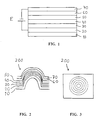
- Figure 1 illustrates a diagrammatic cross section of an OLED structure.
- Figure 2 illustrates a diagrammatic cross section of an OLED structure formed from Figure 1 according to the invention.
- Figure 3 illustrates the contour lines of a formed OLED component illustrated in Figure 2 .
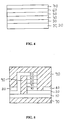
- Figure 4 illustrates a diagrammatic cross section of an alternative OLED structure.
- Figure 5 illustrates one possibility to arrange the electrode connections of an OLED component onto the same level.
- Figure 6 illustrates a modification of the structure in Figure 5 .
- Figure 7 illustrates a situation in which several separate OLED components have been placed on one substrate.
- Figure 8 illustrates a situation in which the OLED structure is formed of a combination of two separate films.
- Figure 9 illustrates an alternative situation in which several separate OLED components have been placed on one substrate.
- Figure 10 illustrates the results of a test in which the luminance of an OLED component formed according to the invention was measured as a function of the voltage.
- Figure 1 illustrates an example of an OLED structure formed of several layers.
- the OLED layers were formed on a substrate 10, and they comprise a first electrode 20 on top of the substrate 10, a hole injecting layer, or electrically conductive polymer layer 30, on top of the first electrodes 20, a hole transporting layer 40 on top of the electrically conductive polymer layer 30, a light emitting layer 50 on top of the hole transporting layer 40, an electron transporting layer 60 on top of the light emitting layer 50, and a second electrode 70 on top of the electron transporting layer 60.
- the power supply E which supplies voltage for the OLED structure is connected so that the positive pole of the power supply E is connected to the first electrode 20, or anode, and the negative pole of the power supply E is connected to the second electrode 70, or cathode.
- the structure illustrated in Figure 1 may be a matrix display element the size of one pixel, or it may be a large surface which is used for background lighting.
- the material of the substrate 10 is flexible and endures forming. Suitable materials are, for example, polyethylene terephthalate (PET), polyester (PE), polycarbonate (PC), polypropylene (PP), acrylate, amorphous glass or a combination PC/PE.
- the substrate may also be formed of an electrically conductive polymer film, for example, polyaniline (PANI) or polytiophene (PT) or their derivates.
- the thickness of the substrate layer 10 is normally within the range 10-1000 ⁇ m, advantageously within the range 10-200 ⁇ m.
- the first electrode 20, or anode must be chosen so that it endures forming. Suitable materials are, for example, indium tin oxide (ITO), polyaniline (PANI) or a thin transparent metal film. ITO's transparency is usually in the range of 80-95%. The thickness of the first electrode 20 is normally approximately 50 nm.
- the hole injecting that is, electrically conductive polymer layer 30
- the thickness of the electrically conductive polymer layer 30 is normally approximately 50 nm.
- the hole transferring layer 40 may be for example N,N'-diphenyle-N,N-bis(3-methylphenyle)-1,1'-bifenyle-4,4'-diamine, that is TPD.
- the thickness of the hole transferring layer 40 is normally approximately 50 nm.
- the light emitting layer 50 may be, for example, of semiconducting organic materials, such as polymers and molecules the molecular orbital structure of which enables exciting the electrons into higher excitation which is then discharged as electromagnetic radiation.
- semiconducting organic materials such as polymers and molecules the molecular orbital structure of which enables exciting the electrons into higher excitation which is then discharged as electromagnetic radiation.
- Such materials are, for instance, tri(8-hydroxyquinoline)aluminium (III), that is, Alq and poly-(2- methoxy-5-(2'-ethylhexyloxy)-1,4-phenylenevinylene), that is MEH-PPV.
- the thickness of the light emitting layer 50 is normally approximately 60 nm.
- the electron transferring layer 60 may be formed, for example, of compounds LiF or CsF.
- the thickness of the electron transferring layer 60 is normally only approximately 0.8 nm. This electron transferring layer functions as a sort of protective layer, and it prevents the light emitting layer 50 from interacting destructively with the OLED.
- the second electrode 70 may be formed of a metal. Suitable metals are aluminium (Al), magnesium/silver (Mg/Ag), calsium (Ca), lithium (Li), gold (Au) and copper (Cu) or a combination of them.
- the thickness of the second electrode 50 is normally approximately 50 nm.
- the forming properties of the OLED structure may also be improved by inserting a substrate film with good forming properties below the substrate 10.
- Figures 2 and 3 illustrate an OLED component according to the invention, which is formed into an area 200, which is ascended from the plane surface, with a plastic forming method known per se.
- Figure 3 illustrates the contour lines of the OLED component illustrated in Figure 2 from a top view.
- Figures 2 and 3 illustrate corresponding structure layers with Figure 1 .
- the OLED area which is ascended from the plane surface may be, for example, hemispherical.
- the OLED area ascended from the plane surface is constructed by forming the plane OLED film in a plastic forming process by vacuum forming, pressure forming or compression forming, and by cutting the formed piece into desired shape if necessary. The cutting may be performed, for example, with cutters or a die cutting method.
- the structure layers of the OLED film must maintain their functionality in the forming so that the electrodes 20, 70 are still conductive and the light emitting layer 50 maintains its emitting capability.
- the OLED film may be fabricated so that the light emitting area forms a desired plane pattern. This may be accomplished in the context of the OLED film fabrication so that, for example, the light emitting layer 50 is formed in the shape of a certain pattern.
- the ready-made plane OLED film may also be cut into the desired shape.
- the patterned OLED film may be formed with a plastic forming method known per se so that one forms areas ascended from the plane surface into it. When one applies injection moulding in the fabrication, one is also able to produce packaging or protection for the product.
- the OLED structure with forming properties enables the fabrication of a formable OLED film or roll, and its insertion into an already formed product.
- Figure 4 illustrates an alternative OLED structure.
- the substrate 10 and the first electrode 20 have been combined into one layer.
- the substrate 10 is then of a netlike material, into which electrically conductive polymer has been impregnated as the anode.
- the netlike substrate material may be comprised of, for example, paper, and the anode material may be for instance PANI.
- Figure 5 illustrates a possibility to arrange the electrode connections of an OLED component on the same level.
- the second electrode 70 has here been brought down onto the substrate 10, whereas the connections of the first electrode 20 and the second electrode 70 are located primarily on the same level.
- the electrodes 20, 70 were each connected into its own conductor film 80, with the aid of which the power supply may be connected to the structure.
- the conductor film may be PANI, Ag or Au.
- the figure shows also a covering 90, with which the structure is protected.
- the protective material 90 may be comprised of polymer layers, for example, of acrylate, which are evaporated in vacuum over the OLED structure and below the substrate layer 10 for protection.
- Figure 6 illustrates an alternative for the structure illustrated in Figure 5 .
- the electrically conductive polymer layer 30 has also been arranged between substrate 10 and the horizontal part of the down-brought cathode 70. This way the bending properties of the area outside the actual OLED component may be improved.
- FIG 7 illustrates a situation in which several separate OLED components OL1, OL2, OL3 have been formed over a shared substrate 10.
- Each OLED component OL1, OL2, OL3 comprises here the layer structure, or an anode 20, an electrically conductive polymer layer 30, a hole transferring layer 40, a light emitting layer 50, an electron transferring layer 60 and a cathode 70 mentioned above in Figures 1 , 4 , 5 and 6 .
- the distance d1, d2 of each OLED component from the next OLED component may vary depending on the requirements, and the surface area A1, A2 and shape of each OLED component may also vary depending on the requirements. This way a desired pattern composed of separate OLED components may be formed on the shared substrate 10.
- the areas between the OLED components OL1, OL2, OL3 may be formed with extensive force, for example so that one forms sharp 90-degree folds into the points in question, and one exerts lighter forming onto areas including OLED components OL1, OL2, OL3.
- Each OLED component OL1, OL2, OL3, the anodes 20 and the cathodes 70 may be connected to the power supply or supplies, either so that all OLED components OL1, OL2, OL3 are controlled simultaneously or so that each OLED component OL1, OL2, OL3 is controlled separately.
- OLED components OL1, OL2, OL3 may form a ring pattern so that OL1 forms the innermost ring, OL2 forms the next ring and OL3 the outmost ring.
- Figure 8 illustrates a situation in which, like in Figure 7 , several separate OLED components OL1, OL2, OL3 are formed over a shared substrate 10. Over the substrate 10 or in the substrate 10 itself, one shared anode 20 was also formed. In addition to this, an area of electrically conductive material JM was formed over the second substrate 10. When the structures are combined, the electrically conductive material area JM settles on top of the cathodes 70 on top of the OLED components OL1, OL2, OL3, and form an electric connection between the mentioned cathodes 70. After combining an OLED structure is produced, in which there are several separate OLED components OL3, OL2, OL3 so that all OLED components are controlled via the shared anode 20 and the shared cathode 70.
- the electrically conductive material JM may be Al, Au, Ag or an electrically conductive polymer, such as PANI, or a combination of them, such as Ag+PANI.
- the situation may naturally be arranged as such that only specified OLED components are combined with the electrically conductive material JM. This way one may form a desired pattern or desired patterns of OLED components, which may be controlled separately.
- Figure 9 illustrated a situation in which oxygen and/or moisture removing material 100 was inserted on OLED areas OL1, OL2, OL3 and/or between them. This arrangement is also protected with a laminate film 110.
- Figure 10 illustrates the results of a test in which the luminance of the OLED component according to the invention was measured as a function of voltage.
- the luminance is presented on the Y axis in relative units (a.u., arbitrary units).
- the measurements of the unformed OLED structure are illustrated with circles, and the measurements of the formed OLED component are illustrated with squares.
- Reasons for the decrease of luminance are for instance the degrading of the first electrode 20 or the ITO layer during forming, a change in the emitting layer 50 during thermal treatment, and a change in the dimensions of the whole structure.
- Vacuum forming was used in this test, the temperature was within the range of 100-170 °C and the forming time was approximately 3 minutes.
- An OLED structure according to the invention may be adapted into a desired supply voltage, for example into the range of 1-5V generally used in mobile phones.
- the power supply may be, for example, batteries manufactured by a printing method, which are known for instance from US patent 5,652,043 .
- the products fabricated with the method according to the invention are of simple design, whereas their fabrication is economical, and they apply well, for example, for consumer products.
Landscapes
- Engineering & Computer Science (AREA)
- Manufacturing & Machinery (AREA)
- Mechanical Engineering (AREA)
- Electroluminescent Light Sources (AREA)
- Laminated Bodies (AREA)
- Manufacture Of Macromolecular Shaped Articles (AREA)
- Blow-Moulding Or Thermoforming Of Plastics Or The Like (AREA)
Abstract
Description
- The object of the present invention is an OLED film according to the preamble of
Claim 1. - The object of the present invention is also a method for forming an OLED film according to the preamble of
Claim 4. - The invention relates to organic light emitting diode structures (OLED) which are used, for example, in passive and active matrix displays. An OLED film is usually formed by evaporating OLED layers onto a substrate. OLED layers typically comprise a first electrode, a layer of emitting material and a second electrode as well as intermediate and protective layers. OILED layers may be formed so that they cover the whole substrate, or so that they will form several different OLED components or OLED areas on the substrate.
- From layer-structured OLED structures, one may form large consistent plane surfaces which endure bending so that they can be formed into evenly curved surfaces. Thus, from a plane OLED structure, one is able to form, for example, a curved surface which follows the cylindrical surface below it. The OLED structure deflects thus only to the direction of the cylindrical surface perimeter, whereas the material structure of electrodes in the OLED structure remains unbroken. Then the electrical conductivity of electrodes in the direction of the plane surface is maintained. Such structures may be used in, for example, background lighting.
- The
FI patent application 981731 - The
EP patent publication 1065737 presents an OLED structure in which an electron hole injecting layer has been placed between the anode and the light emitting layer. On the other hand, an electron-emitting layer has been placed between the cathode and the light emitting material. - The
US patent 5,970,318 presents a structure which endures mechanical bending and consists of an OLED and a transistor, and which may be used in flexible displays. This OLED comprises a transparent electrode formed on a substrate, an organic light emitting layer formed on the electrode, and an upper electrode formed on the emitting layer. - The
US patent 6,046,543 presents a reversed OLED structure. This structure comprises a substrate, a polymer layer on top of the substrate, a cathode on top of the polymer layer, an electron transporting layer on top of the cathode, a light emitting layer on top of the electron transporting layer, a hole transporting layer on top of the light emitting layer, a protective layer on top of the hole transporting layer, and an anode on top of the protective layer. - According to the preconception of the persons skilled in the art, a layer-structured OLED structure does not remain unbroken and functional if a plane OLED structure is bent in the direction of several axes pointing to different directions in the plane surface. Thus, according to the preconception of the persons skilled in the art, one has not been able to form areas ascended from the level surface into the plane OLED surface, for instance hemispherical areas. This matter has limited the use of the OLED structure in applications in which one could use plane surfaces, and such plane surfaces which curve in the direction of the perimeter of cylindrical surface. OLED structures were not usable in such objects in which the OLED structure should be formed on a surface bending in the direction of several axes, such as on hemisphere.
- According to the preconception of the persons skilled in the art, one has also not been able to form plane OLED structures into pieces of desired shape by cutting, because the anode and the cathode of the OLED stricture were considered to short circuit at the cutting point. Because the thickness of the OLED layers formed on the substrate is only approximately 50 nm, it has been thought that the anode and the cathode will inevitably be in touch with each other at the cutting point
- In principle, an OLED area ascended from a plane OLED surface could be constructed directly by coating OLED layers on a non-flat surface, for example on a hemisphere, but this option is not practical or productive. Then, the non-flat surface which is coated by evaporation should be rotated during coating. In addition, it is difficult to form an even coating on a non-flat rotating surface.
- In the present invention, it was noticed contrary to the preconceptions of the persons skilled in the art that ascended OLED areas may be formed on a plane OLED structure so that the functionality of the OLED structure is maintained.
- In the present invention, it was also noticed contrary to the preconceptions of the persons skilled in the art that pieces of desired shape may be cut from a plane OLED structure so that the functionality of the OLED structure is maintained.
- The principal characteristics of the OLED film according to the invention are presented in the characterising part of
Claim 1. - The principal characteristics of the method according to the invention are presented in the characterising part of
Claim 4. - With the method according to the invention, an ascended area or ascended areas, such as hemispherical areas, may be formed on a plane OLED film, which comprises a substrate and OLED layers formed on it. This structure is produced by forming an OLED known per se, which endures forming, temperature loading and mechanical stress, with forming methods known per se which are suited for forming plastic-like materials, such as vacuum forming, pressure forming, matched-mould forming or their combination in a plastic forming machine. With an OLED film thus produced, one is able to, for example, generate light on a surface of desired shape or use the produced structure for patterning purposes. One may thus utilise an unused non-flat surface or space in, for instance, portable electronics products. Other possible applications for structures according to the invention are, for example, integrated background lights in different consumer goods, such as watches.
- The forming may be done so that only the OLED film is formed, after which the formed OLED film is inserted as a part of the product in which one wishes to utilise the light generated by the OLED component.
- The forming may also be done so that the OLED film is formed together with the product the part of which one wishes the OLED film to become. This could be, for instance, a situation in which one wishes the OLED film to be a part of a plastic piece. Then the OLED film is combined to a plastic blank and both parts are formed together in a plastic forming process.
- In vacuum forming, the plane OLED film is placed over a mould and fastened from its edges to the mould. After this, vacuum is produced to the space between the mould and OLED film, whereas the OLED film sticks onto the surfaces of the mould. Thus, the OLED film is formed to the shape defined by the mould surfaces.
- In pressure forming, the plane OLED film is placed over a mould and fastened from its edges to the mould. The mould is closed with a sealing cover, after which pressure is lead to the space between the cover and the OLED film, whereas the pressure presses the OLED film firmly onto the mould surfaces. The OLED film is thus formed to the shape defined by the mould surfaces. The removal of air from the space between the OLED film and the mould must be arranged. Forming may further be intensified by producing a vacuum in the space between the OLED film and the mould. Then, the vacuum below the OLED film sucks the OLED film closely onto the mould surfaces, and the pressure above the OLED film presses the OLED film closely onto the mould surfaces.
- In matched-mould forming, the OLED film is placed over a female mould and fastened from its edges to the mould. After this, the OLED film is pressed with a male mould into the female mould, wheres the OLED film between the moulds is formed into the shape defined by the moulds.
- In all above-mentioned forming methods, the OLED film is usually preheated into an appropriate temperature before forming, when the forming qualities of the OLED film are improved. Because high temperatures age the OLED film, the heating phase should be short and the used temperature as low as possible. The significance of this problem will constantly decrease as OLED films improve and become more stabile.
- The forming according to the invention, in which the starting point is a plane substrate, into which one has formed one consistent or several separate OLED components, applies extremely well into mass production. The fabrication of a plane film which includes OLEDs is economical and effective, and also forming a ready-made OLED film in the plastic forming process is economical and effective.
- The- invention will now be explained in more detail with reference, to the accompanying drawings, but not limiting the invention to only such details.
-
Figure 1 illustrates a diagrammatic cross section of an OLED structure. -
Figure 2 illustrates a diagrammatic cross section of an OLED structure formed fromFigure 1 according to the invention. -
Figure 3 illustrates the contour lines of a formed OLED component illustrated inFigure 2 . -
Figure 4 illustrates a diagrammatic cross section of an alternative OLED structure. -
Figure 5 illustrates one possibility to arrange the electrode connections of an OLED component onto the same level. -
Figure 6 illustrates a modification of the structure inFigure 5 . -
Figure 7 illustrates a situation in which several separate OLED components have been placed on one substrate. -
Figure 8 illustrates a situation in which the OLED structure is formed of a combination of two separate films. -
Figure 9 illustrates an alternative situation in which several separate OLED components have been placed on one substrate. -
Figure 10 illustrates the results of a test in which the luminance of an OLED component formed according to the invention was measured as a function of the voltage. -
Figure 1 illustrates an example of an OLED structure formed of several layers. The OLED layers were formed on asubstrate 10, and they comprise afirst electrode 20 on top of thesubstrate 10, a hole injecting layer, or electricallyconductive polymer layer 30, on top of thefirst electrodes 20, ahole transporting layer 40 on top of the electricallyconductive polymer layer 30, alight emitting layer 50 on top of thehole transporting layer 40, anelectron transporting layer 60 on top of thelight emitting layer 50, and asecond electrode 70 on top of theelectron transporting layer 60. The power supply E which supplies voltage for the OLED structure is connected so that the positive pole of the power supply E is connected to thefirst electrode 20, or anode, and the negative pole of the power supply E is connected to thesecond electrode 70, or cathode. The structure illustrated inFigure 1 may be a matrix display element the size of one pixel, or it may be a large surface which is used for background lighting. - In the structure of
Figure 1 , light is directed from thelight emitting layer 50 through thehole transporting layer 40, thehole injecting layer 30, thefirst electrode 20 and thesubstrate 10 beneath it. Thus, thelayers light emitting layer 50 must transmit light. Naturally, the situation may also be reversed so that light is directed through thesecond electrode 70. - The material of the
substrate 10 is flexible and endures forming. Suitable materials are, for example, polyethylene terephthalate (PET), polyester (PE), polycarbonate (PC), polypropylene (PP), acrylate, amorphous glass or a combination PC/PE. The substrate may also be formed of an electrically conductive polymer film, for example, polyaniline (PANI) or polytiophene (PT) or their derivates. The thickness of thesubstrate layer 10 is normally within the range 10-1000 µm, advantageously within the range 10-200 µm. - The
first electrode 20, or anode, must be chosen so that it endures forming. Suitable materials are, for example, indium tin oxide (ITO), polyaniline (PANI) or a thin transparent metal film. ITO's transparency is usually in the range of 80-95%. The thickness of thefirst electrode 20 is normally approximately 50 nm. - As the hole injecting, that is, electrically
conductive polymer layer 30, one may use for example polytiophene (PT) and its derivates or polyaniline (PANI) and its derivates. The thickness of the electricallyconductive polymer layer 30 is normally approximately 50 nm. - The
hole transferring layer 40 may be for example N,N'-diphenyle-N,N-bis(3-methylphenyle)-1,1'-bifenyle-4,4'-diamine, that is TPD. The thickness of thehole transferring layer 40 is normally approximately 50 nm. - The
light emitting layer 50 may be, for example, of semiconducting organic materials, such as polymers and molecules the molecular orbital structure of which enables exciting the electrons into higher excitation which is then discharged as electromagnetic radiation. Such materials are, for instance, tri(8-hydroxyquinoline)aluminium (III), that is, Alq and poly-(2- methoxy-5-(2'-ethylhexyloxy)-1,4-phenylenevinylene), that is MEH-PPV. The thickness of thelight emitting layer 50 is normally approximately 60 nm. - The
electron transferring layer 60 may be formed, for example, of compounds LiF or CsF. The thickness of theelectron transferring layer 60 is normally only approximately 0.8 nm. This electron transferring layer functions as a sort of protective layer, and it prevents thelight emitting layer 50 from interacting destructively with the OLED. - The
second electrode 70, or cathode, may be formed of a metal. Suitable metals are aluminium (Al), magnesium/silver (Mg/Ag), calsium (Ca), lithium (Li), gold (Au) and copper (Cu) or a combination of them. The thickness of thesecond electrode 50 is normally approximately 50 nm. - With the above mentioned materials, one is able to produce a formable OLED structure. With the electrically
conductive polymer 30 on theanode 20, the electrical conductivity of theanode 20 is secured in a horizontal direction in a situation, in which theanode 20 is degraded. The electricallyconductive polymer 30 then vertically forms an electricity conductive bridge between the degraded electrode areas. After forming, both theanode 20 and thecathode 70 may be degraded, but still preserve their functionality. - The forming properties of the OLED structure may also be improved by inserting a substrate film with good forming properties below the
substrate 10. -
Figures 2 and 3 illustrate an OLED component according to the invention, which is formed into anarea 200, which is ascended from the plane surface, with a plastic forming method known per se.Figure 3 illustrates the contour lines of the OLED component illustrated inFigure 2 from a top view.Figures 2 and 3 illustrate corresponding structure layers withFigure 1 . - The OLED area which is ascended from the plane surface may be, for example, hemispherical. The OLED area ascended from the plane surface is constructed by forming the plane OLED film in a plastic forming process by vacuum forming, pressure forming or compression forming, and by cutting the formed piece into desired shape if necessary. The cutting may be performed, for example, with cutters or a die cutting method. The structure layers of the OLED film must maintain their functionality in the forming so that the
electrodes light emitting layer 50 maintains its emitting capability. - The OLED film may be fabricated so that the light emitting area forms a desired plane pattern. This may be accomplished in the context of the OLED film fabrication so that, for example, the
light emitting layer 50 is formed in the shape of a certain pattern. The ready-made plane OLED film may also be cut into the desired shape. After this, the patterned OLED film may be formed with a plastic forming method known per se so that one forms areas ascended from the plane surface into it. When one applies injection moulding in the fabrication, one is also able to produce packaging or protection for the product. - The OLED structure with forming properties enables the fabrication of a formable OLED film or roll, and its insertion into an already formed product.
-
Figure 4 illustrates an alternative OLED structure. In this alternative, thesubstrate 10 and thefirst electrode 20 have been combined into one layer. Thesubstrate 10 is then of a netlike material, into which electrically conductive polymer has been impregnated as the anode. The netlike substrate material may be comprised of, for example, paper, and the anode material may be for instance PANI. -
Figure 5 illustrates a possibility to arrange the electrode connections of an OLED component on the same level. Thesecond electrode 70 has here been brought down onto thesubstrate 10, whereas the connections of thefirst electrode 20 and thesecond electrode 70 are located primarily on the same level. Theelectrodes own conductor film 80, with the aid of which the power supply may be connected to the structure. The conductor film may be PANI, Ag or Au. The figure shows also a covering 90, with which the structure is protected. Theprotective material 90 may be comprised of polymer layers, for example, of acrylate, which are evaporated in vacuum over the OLED structure and below thesubstrate layer 10 for protection. -
Figure 6 illustrates an alternative for the structure illustrated inFigure 5 . In this alternative, the electricallyconductive polymer layer 30 has also been arranged betweensubstrate 10 and the horizontal part of the down-broughtcathode 70. This way the bending properties of the area outside the actual OLED component may be improved. -
Figure 7 illustrates a situation in which several separate OLED components OL1, OL2, OL3 have been formed over a sharedsubstrate 10. Each OLED component OL1, OL2, OL3 comprises here the layer structure, or ananode 20, an electricallyconductive polymer layer 30, ahole transferring layer 40, alight emitting layer 50, anelectron transferring layer 60 and acathode 70 mentioned above inFigures 1 ,4 ,5 and6 . The distance d1, d2 of each OLED component from the next OLED component may vary depending on the requirements, and the surface area A1, A2 and shape of each OLED component may also vary depending on the requirements. This way a desired pattern composed of separate OLED components may be formed on the sharedsubstrate 10. With such structure, the forming properties of the OLED film may further be improved. The areas between the OLED components OL1, OL2, OL3 may be formed with extensive force, for example so that one forms sharp 90-degree folds into the points in question, and one exerts lighter forming onto areas including OLED components OL1, OL2, OL3. Each OLED component OL1, OL2, OL3, theanodes 20 and thecathodes 70 may be connected to the power supply or supplies, either so that all OLED components OL1, OL2, OL3 are controlled simultaneously or so that each OLED component OL1, OL2, OL3 is controlled separately. For instance, OLED components OL1, OL2, OL3 may form a ring pattern so that OL1 forms the innermost ring, OL2 forms the next ring and OL3 the outmost ring. -
Figure 8 illustrates a situation in which, like inFigure 7 , several separate OLED components OL1, OL2, OL3 are formed over a sharedsubstrate 10. Over thesubstrate 10 or in thesubstrate 10 itself, one sharedanode 20 was also formed. In addition to this, an area of electrically conductive material JM was formed over thesecond substrate 10. When the structures are combined, the electrically conductive material area JM settles on top of thecathodes 70 on top of the OLED components OL1, OL2, OL3, and form an electric connection between the mentionedcathodes 70. After combining an OLED structure is produced, in which there are several separate OLED components OL3, OL2, OL3 so that all OLED components are controlled via the sharedanode 20 and the sharedcathode 70. The electrically conductive material JM may be Al, Au, Ag or an electrically conductive polymer, such as PANI, or a combination of them, such as Ag+PANI. The situation may naturally be arranged as such that only specified OLED components are combined with the electrically conductive material JM. This way one may form a desired pattern or desired patterns of OLED components, which may be controlled separately. -
Figure 9 illustrated a situation in which oxygen and/ormoisture removing material 100 was inserted on OLED areas OL1, OL2, OL3 and/or between them. This arrangement is also protected with alaminate film 110. -
Figure 10 illustrates the results of a test in which the luminance of the OLED component according to the invention was measured as a function of voltage. The luminance is presented on the Y axis in relative units (a.u., arbitrary units). The measurements of the unformed OLED structure are illustrated with circles, and the measurements of the formed OLED component are illustrated with squares. In the tests made, it was observed that after forming the luminance of the OLED structure decreased only approximately 10-20%, that is, the luminance is sufficient enough for many kinds of applications. Reasons for the decrease of luminance are for instance the degrading of thefirst electrode 20 or the ITO layer during forming, a change in the emittinglayer 50 during thermal treatment, and a change in the dimensions of the whole structure. Thus, the micro cracks invisible to the eye, which were produced during forming, do not make the product totally inoperative. Vacuum forming was used in this test, the temperature was within the range of 100-170 °C and the forming time was approximately 3 minutes. - An OLED structure according to the invention may be adapted into a desired supply voltage, for example into the range of 1-5V generally used in mobile phones. Within this range, the power supply may be, for example, batteries manufactured by a printing method, which are known for instance from
US patent 5,652,043 . - The products fabricated with the method according to the invention are of simple design, whereas their fabrication is economical, and they apply well, for example, for consumer products.
- The scope of the invention is defined by the following claims.
Claims (8)
- An OLED film is formed of at least one layer-structured OLED component (OL1, OL2, OL3) formed on a substrate (10), which OLED component comprises a first electrode (20), an electrically conductive polymer (30), a light emitting material (40) and a second electrode (50), as well as intermediate and protective layers (40, 60, 80, 90, 100, 110), characterised in that the said at least one OLED component (OL1, OL2; OL3) comprises at least one OLED area ascended from the plane film.
- An OLED film according to Claim 1, characterised in that one consistent layer-structured OLED component which covers the whole substrate (10) is formed on the substrate (10), and that the said OLED component comprises at least one OLED area ascended from the plane film.
- An OLED film according to Claim 1, characterised in that at least two separate layer-structured OLED components (OL1, OL2, OL3) are formed on the substrate (10), and that at least one of these OLED components (OL3, OL2, OL3) comprises at least one OLED area ascended from the plane film.
- A method for forming an OLED film according to claim 1, comprising forming at least one layer-structured plane OLED component (OL3, OL2, OL3) on a plane substrate (10) with a method know per se, which OLED component comprises a first electrode (20), an electrically conductive polymer (30), a light emitting material (50) and a second electrode (70), as well as intermediate and protective layers (40, 60, 80, 90, 100, 110), characterised by forming the plane OLED film comprising the substrate (10) and the at least one OLED component (OL1, OL2, OL3) in a plastic forming process know per se by using vacuum, pressure, compression or a combination of these so that at least one OLED area ascended from the plane OLED component (OL1, OL2, OL3) being formed on the plane OLED film
- A method according to Claim 4, characterised by forming one consistent layer-structured OLED component which covers the whole substrate (10) on the substrate (10), and by foaming the thus formed plane OLED film is formed in a plastic forming process know per se by using vacuum, pressure, compression or a combination of these so that at least one OLED area ascended from the plane OLED component (OL1, OL2, OL3) being formed in the plane OLED film.
- A method according to Claim 1, characterised by forming at least two separate layer-structured OLED components (OL1, OL2; OL3) on the substrate (10), and by forming the thus formed plane OLED film in a plastic forming process known per se by using vacuum, pressure, compression or a combination of these so that at least one OLED area ascended from the plane OLED component (OL1, OL2, OL3) being formed in the plane OLED film.
- A method according to one of Claims 4-6, characterised by forming the formed layer-structured plane OLED film together with a plane plastic piece in a plastic forming process known per se by using vacuum, pressure, compression or a combination of these so that the substrate (10) and the OLED film are formed as a part of the plastic piece, and at least one OLED area ascended from the plane structure being formed in the combined OLED and plastic piece structure.
- A method according to one of Claims 4-7, characterised by cutting the OLED film formed in the plastic forming process is cut to desired shape with cutters or a die cutting method while maintaining the functionality of the OLED film.
Applications Claiming Priority (3)
| Application Number | Priority Date | Filing Date | Title |
|---|---|---|---|
| FI20011483A FI110675B (en) | 2001-07-06 | 2001-07-06 | Method of forming an organic light emitting diode |
| FI20011483 | 2001-07-06 | ||
| PCT/FI2002/000547 WO2003004252A1 (en) | 2001-07-06 | 2002-06-20 | Method for forming an oled film and an oled film |
Publications (2)
| Publication Number | Publication Date |
|---|---|
| EP1404507A1 EP1404507A1 (en) | 2004-04-07 |
| EP1404507B1 true EP1404507B1 (en) | 2009-06-03 |
Family
ID=8561608
Family Applications (1)
| Application Number | Title | Priority Date | Filing Date |
|---|---|---|---|
| EP02743307A Expired - Lifetime EP1404507B1 (en) | 2001-07-06 | 2002-06-20 | Oled film and method for its forming |
Country Status (8)
| Country | Link |
|---|---|
| US (1) | US20040238856A1 (en) |
| EP (1) | EP1404507B1 (en) |
| JP (1) | JP2004533351A (en) |
| KR (1) | KR20040025694A (en) |
| AT (1) | ATE432809T1 (en) |
| DE (1) | DE60232514D1 (en) |
| FI (1) | FI110675B (en) |
| WO (1) | WO2003004252A1 (en) |
Families Citing this family (8)
| Publication number | Priority date | Publication date | Assignee | Title |
|---|---|---|---|---|
| US7259391B2 (en) * | 2004-12-22 | 2007-08-21 | General Electric Company | Vertical interconnect for organic electronic devices |
| US20090163256A1 (en) * | 2007-12-21 | 2009-06-25 | Motorola, Inc. | Translucent single layer touch screen devices having vertically oriented pattern traces |
| CN102027615A (en) * | 2008-03-26 | 2011-04-20 | 皇家飞利浦电子股份有限公司 | Light emitting diode device |
| US20120051067A1 (en) * | 2010-08-24 | 2012-03-01 | Key Plastics L.L.C. | Lighting display and method of manufacturing same |
| DE102013020782A1 (en) * | 2013-12-13 | 2015-06-18 | GM Global Technology Operations, LLC (n.d. Ges. d. Staates Delaware) | Vehicle with light indicator |
| CN104112823A (en) * | 2014-06-30 | 2014-10-22 | 上海天马有机发光显示技术有限公司 | White organic light-emitting device |
| DE102017214388A1 (en) * | 2017-08-18 | 2019-02-21 | Bayerische Motoren Werke Aktiengesellschaft | Method for producing a functional interior component for a vehicle |
| EP3922433A1 (en) * | 2020-06-12 | 2021-12-15 | Nederlandse Organisatie voor toegepast- natuurwetenschappelijk Onderzoek TNO | Thermoformed device with oled display and method of fabrication |
Family Cites Families (15)
| Publication number | Priority date | Publication date | Assignee | Title |
|---|---|---|---|---|
| US5059861A (en) * | 1990-07-26 | 1991-10-22 | Eastman Kodak Company | Organic electroluminescent device with stabilizing cathode capping layer |
| US6465951B1 (en) * | 1992-12-16 | 2002-10-15 | Durel Corporation | Electroluminescent lamp devices and their manufacture |
| US5719467A (en) * | 1995-07-27 | 1998-02-17 | Hewlett-Packard Company | Organic electroluminescent device |
| US5652043A (en) * | 1995-12-20 | 1997-07-29 | Baruch Levanon | Flexible thin layer open electrochemical cell |
| US5806389A (en) * | 1996-06-13 | 1998-09-15 | Durel Corporation | EL lamp with beveled edge |
| US5834893A (en) * | 1996-12-23 | 1998-11-10 | The Trustees Of Princeton University | High efficiency organic light emitting devices with light directing structures |
| US6046543A (en) * | 1996-12-23 | 2000-04-04 | The Trustees Of Princeton University | High reliability, high efficiency, integratable organic light emitting devices and methods of producing same |
| US5998803A (en) * | 1997-05-29 | 1999-12-07 | The Trustees Of Princeton University | Organic light emitting device containing a hole injection enhancement layer |
| KR100248392B1 (en) * | 1997-05-15 | 2000-09-01 | 정선종 | Organic Active Driving Electroluminescent Device Combined with Organic Field Effect Transistor and Fabrication Method |
| US6013538A (en) * | 1997-11-24 | 2000-01-11 | The Trustees Of Princeton University | Method of fabricating and patterning OLEDs |
| FI109944B (en) * | 1998-08-11 | 2002-10-31 | Valtion Teknillinen | Optoelectronic component and manufacturing method |
| KR100683050B1 (en) * | 1999-06-28 | 2007-02-15 | 모토로라 인코포레이티드 | Organic electroluminescent devices |
| US6566808B1 (en) * | 1999-12-22 | 2003-05-20 | General Electric Company | Luminescent display and method of making |
| US6580090B2 (en) * | 2001-06-22 | 2003-06-17 | International Business Machines Corporation | Organic light-emitting devices |
| US6596784B1 (en) * | 2002-05-07 | 2003-07-22 | Nien Made Enterprise Co., Ltd. | Strengthened thermoplastic for window coverings |
-
2001
- 2001-07-06 FI FI20011483A patent/FI110675B/en not_active IP Right Cessation
-
2002
- 2002-06-20 EP EP02743307A patent/EP1404507B1/en not_active Expired - Lifetime
- 2002-06-20 DE DE60232514T patent/DE60232514D1/en not_active Expired - Lifetime
- 2002-06-20 JP JP2003510243A patent/JP2004533351A/en active Pending
- 2002-06-20 US US10/482,920 patent/US20040238856A1/en not_active Abandoned
- 2002-06-20 WO PCT/FI2002/000547 patent/WO2003004252A1/en not_active Ceased
- 2002-06-20 AT AT02743307T patent/ATE432809T1/en not_active IP Right Cessation
- 2002-06-20 KR KR10-2004-7000091A patent/KR20040025694A/en not_active Ceased
Also Published As
| Publication number | Publication date |
|---|---|
| FI110675B (en) | 2003-03-14 |
| JP2004533351A (en) | 2004-11-04 |
| FI20011483A0 (en) | 2001-07-06 |
| EP1404507A1 (en) | 2004-04-07 |
| US20040238856A1 (en) | 2004-12-02 |
| KR20040025694A (en) | 2004-03-24 |
| DE60232514D1 (en) | 2009-07-16 |
| ATE432809T1 (en) | 2009-06-15 |
| WO2003004252A1 (en) | 2003-01-16 |
Similar Documents
| Publication | Publication Date | Title |
|---|---|---|
| US7632165B2 (en) | Organic electro-optic device and method for making the same | |
| KR100726061B1 (en) | A plurality of electrically connected organic optoelectronic devices and methods of providing the same | |
| EP2557899B1 (en) | Transparent electrode and organic electronic element using same | |
| EP2494619B1 (en) | A light-emitting electrochemical device, a system comprising such a device | |
| US20120276734A1 (en) | Method of manufacturing an opto-electric device | |
| WO2001006577A8 (en) | Cavity-emission electroluminescent device and method for forming the device | |
| JP2001237065A (en) | Polymer EL device and manufacturing method thereof | |
| JPH11503868A (en) | Manufacture of organic light emitting devices | |
| NO330298B1 (en) | Electroluminescent device and process for its preparation | |
| EP2294642B1 (en) | Method for producing an organic electronic component | |
| CN101379632A (en) | Large area organic electronic devices and methods of fabricating the same | |
| US20040238856A1 (en) | Method for forming an oled film and an oled film | |
| WO2003050895A1 (en) | Improved production of electroluminescent devices | |
| Kim et al. | Recent progress on the development of intrinsically stretchable electroluminescent devices | |
| EP3453059B1 (en) | Method for fabricating a solar module | |
| EP2382677B1 (en) | Electro-optic device and method for manufacturing the same | |
| TW201129240A (en) | Organic electroluminescent devices | |
| WO2004068584A1 (en) | Light-emitting devices | |
| US12186945B2 (en) | Method for manufacturing an opto-electronic component substrate | |
| EP1681734A1 (en) | Optoelectronic device and method for producing the same | |
| CN116507179A (en) | Organic photoelectric device and preparation method thereof | |
| CN115148922A (en) | Flexible OLED device product, flexible OLED device and preparation method thereof | |
| HK1061605B (en) | Push-button switch member and method of manufacturing same | |
| Bhattacharya | Thin film electronic arrays on three-dimensional surfaces | |
| HK1061605A1 (en) | Push-button switch member and method of manufacturing same |
Legal Events
| Date | Code | Title | Description |
|---|---|---|---|
| PUAI | Public reference made under article 153(3) epc to a published international application that has entered the european phase |
Free format text: ORIGINAL CODE: 0009012 |
|
| 17P | Request for examination filed |
Effective date: 20031208 |
|
| AK | Designated contracting states |
Kind code of ref document: A1 Designated state(s): AT BE CH CY DE DK ES FI FR GB GR IE IT LI LU MC NL PT SE TR |
|
| AX | Request for extension of the european patent |
Extension state: AL LT LV MK RO SI |
|
| RIN1 | Information on inventor provided before grant (corrected) |
Inventor name: MAEKELAE, TAPIO Inventor name: ISOTALO, HEIKKI Inventor name: LAPPALAINEN, JUKKA |
|
| RIN1 | Information on inventor provided before grant (corrected) |
Inventor name: MAEKELAE, TAPIO Inventor name: LAPPALAINEN, JUKKA Inventor name: ISOTALO, HEIKKI |
|
| 17Q | First examination report despatched |
Effective date: 20080205 |
|
| GRAP | Despatch of communication of intention to grant a patent |
Free format text: ORIGINAL CODE: EPIDOSNIGR1 |
|
| RTI1 | Title (correction) |
Free format text: OLED FILM AND METHOD FOR ITS FORMING |
|
| GRAS | Grant fee paid |
Free format text: ORIGINAL CODE: EPIDOSNIGR3 |
|
| GRAA | (expected) grant |
Free format text: ORIGINAL CODE: 0009210 |
|
| AK | Designated contracting states |
Kind code of ref document: B1 Designated state(s): AT BE CH CY DE DK ES FI FR GB GR IE IT LI LU MC NL PT SE TR |
|
| REG | Reference to a national code |
Ref country code: GB Ref legal event code: FG4D |
|
| REG | Reference to a national code |
Ref country code: CH Ref legal event code: EP |
|
| REG | Reference to a national code |
Ref country code: IE Ref legal event code: FG4D |
|
| REF | Corresponds to: |
Ref document number: 60232514 Country of ref document: DE Date of ref document: 20090716 Kind code of ref document: P |
|
| PG25 | Lapsed in a contracting state [announced via postgrant information from national office to epo] |
Ref country code: FI Free format text: LAPSE BECAUSE OF FAILURE TO SUBMIT A TRANSLATION OF THE DESCRIPTION OR TO PAY THE FEE WITHIN THE PRESCRIBED TIME-LIMIT Effective date: 20090603 Ref country code: AT Free format text: LAPSE BECAUSE OF FAILURE TO SUBMIT A TRANSLATION OF THE DESCRIPTION OR TO PAY THE FEE WITHIN THE PRESCRIBED TIME-LIMIT Effective date: 20090603 |
|
| NLV1 | Nl: lapsed or annulled due to failure to fulfill the requirements of art. 29p and 29m of the patents act | ||
| PG25 | Lapsed in a contracting state [announced via postgrant information from national office to epo] |
Ref country code: SE Free format text: LAPSE BECAUSE OF FAILURE TO SUBMIT A TRANSLATION OF THE DESCRIPTION OR TO PAY THE FEE WITHIN THE PRESCRIBED TIME-LIMIT Effective date: 20090903 Ref country code: NL Free format text: LAPSE BECAUSE OF FAILURE TO SUBMIT A TRANSLATION OF THE DESCRIPTION OR TO PAY THE FEE WITHIN THE PRESCRIBED TIME-LIMIT Effective date: 20090603 |
|
| PG25 | Lapsed in a contracting state [announced via postgrant information from national office to epo] |
Ref country code: ES Free format text: LAPSE BECAUSE OF FAILURE TO SUBMIT A TRANSLATION OF THE DESCRIPTION OR TO PAY THE FEE WITHIN THE PRESCRIBED TIME-LIMIT Effective date: 20090914 Ref country code: MC Free format text: LAPSE BECAUSE OF NON-PAYMENT OF DUE FEES Effective date: 20090630 |
|
| REG | Reference to a national code |
Ref country code: CH Ref legal event code: PL |
|
| PG25 | Lapsed in a contracting state [announced via postgrant information from national office to epo] |
Ref country code: BE Free format text: LAPSE BECAUSE OF FAILURE TO SUBMIT A TRANSLATION OF THE DESCRIPTION OR TO PAY THE FEE WITHIN THE PRESCRIBED TIME-LIMIT Effective date: 20090603 |
|
| PG25 | Lapsed in a contracting state [announced via postgrant information from national office to epo] |
Ref country code: PT Free format text: LAPSE BECAUSE OF FAILURE TO SUBMIT A TRANSLATION OF THE DESCRIPTION OR TO PAY THE FEE WITHIN THE PRESCRIBED TIME-LIMIT Effective date: 20091003 |
|
| PLBE | No opposition filed within time limit |
Free format text: ORIGINAL CODE: 0009261 |
|
| STAA | Information on the status of an ep patent application or granted ep patent |
Free format text: STATUS: NO OPPOSITION FILED WITHIN TIME LIMIT |
|
| PG25 | Lapsed in a contracting state [announced via postgrant information from national office to epo] |
Ref country code: CH Free format text: LAPSE BECAUSE OF NON-PAYMENT OF DUE FEES Effective date: 20090630 Ref country code: LI Free format text: LAPSE BECAUSE OF NON-PAYMENT OF DUE FEES Effective date: 20090630 Ref country code: DK Free format text: LAPSE BECAUSE OF FAILURE TO SUBMIT A TRANSLATION OF THE DESCRIPTION OR TO PAY THE FEE WITHIN THE PRESCRIBED TIME-LIMIT Effective date: 20090603 Ref country code: IE Free format text: LAPSE BECAUSE OF NON-PAYMENT OF DUE FEES Effective date: 20090620 |
|
| 26N | No opposition filed |
Effective date: 20100304 |
|
| PG25 | Lapsed in a contracting state [announced via postgrant information from national office to epo] |
Ref country code: GR Free format text: LAPSE BECAUSE OF FAILURE TO SUBMIT A TRANSLATION OF THE DESCRIPTION OR TO PAY THE FEE WITHIN THE PRESCRIBED TIME-LIMIT Effective date: 20090904 |
|
| PG25 | Lapsed in a contracting state [announced via postgrant information from national office to epo] |
Ref country code: IT Free format text: LAPSE BECAUSE OF FAILURE TO SUBMIT A TRANSLATION OF THE DESCRIPTION OR TO PAY THE FEE WITHIN THE PRESCRIBED TIME-LIMIT Effective date: 20090603 |
|
| PG25 | Lapsed in a contracting state [announced via postgrant information from national office to epo] |
Ref country code: LU Free format text: LAPSE BECAUSE OF NON-PAYMENT OF DUE FEES Effective date: 20090620 |
|
| PG25 | Lapsed in a contracting state [announced via postgrant information from national office to epo] |
Ref country code: TR Free format text: LAPSE BECAUSE OF FAILURE TO SUBMIT A TRANSLATION OF THE DESCRIPTION OR TO PAY THE FEE WITHIN THE PRESCRIBED TIME-LIMIT Effective date: 20090603 |
|
| PG25 | Lapsed in a contracting state [announced via postgrant information from national office to epo] |
Ref country code: CY Free format text: LAPSE BECAUSE OF FAILURE TO SUBMIT A TRANSLATION OF THE DESCRIPTION OR TO PAY THE FEE WITHIN THE PRESCRIBED TIME-LIMIT Effective date: 20090603 |
|
| REG | Reference to a national code |
Ref country code: FR Ref legal event code: PLFP Year of fee payment: 14 |
|
| REG | Reference to a national code |
Ref country code: FR Ref legal event code: PLFP Year of fee payment: 15 |
|
| PGFP | Annual fee paid to national office [announced via postgrant information from national office to epo] |
Ref country code: GB Payment date: 20161028 Year of fee payment: 15 Ref country code: FR Payment date: 20161110 Year of fee payment: 15 Ref country code: DE Payment date: 20161110 Year of fee payment: 15 |
|
| REG | Reference to a national code |
Ref country code: DE Ref legal event code: R119 Ref document number: 60232514 Country of ref document: DE |
|
| GBPC | Gb: european patent ceased through non-payment of renewal fee |
Effective date: 20170620 |
|
| REG | Reference to a national code |
Ref country code: FR Ref legal event code: ST Effective date: 20180228 |
|
| PG25 | Lapsed in a contracting state [announced via postgrant information from national office to epo] |
Ref country code: DE Free format text: LAPSE BECAUSE OF NON-PAYMENT OF DUE FEES Effective date: 20180103 Ref country code: GB Free format text: LAPSE BECAUSE OF NON-PAYMENT OF DUE FEES Effective date: 20170620 |
|
| PG25 | Lapsed in a contracting state [announced via postgrant information from national office to epo] |
Ref country code: FR Free format text: LAPSE BECAUSE OF NON-PAYMENT OF DUE FEES Effective date: 20170630 |