EP1404131A1 - Interface circuit for television tuner - Google Patents
Interface circuit for television tuner Download PDFInfo
- Publication number
- EP1404131A1 EP1404131A1 EP20030028456 EP03028456A EP1404131A1 EP 1404131 A1 EP1404131 A1 EP 1404131A1 EP 20030028456 EP20030028456 EP 20030028456 EP 03028456 A EP03028456 A EP 03028456A EP 1404131 A1 EP1404131 A1 EP 1404131A1
- Authority
- EP
- European Patent Office
- Prior art keywords
- pin
- pins
- tuner block
- tuner
- block
- Prior art date
- Legal status (The legal status is an assumption and is not a legal conclusion. Google has not performed a legal analysis and makes no representation as to the accuracy of the status listed.)
- Granted
Links
Images




Classifications
-
- H—ELECTRICITY
- H04—ELECTRIC COMMUNICATION TECHNIQUE
- H04N—PICTORIAL COMMUNICATION, e.g. TELEVISION
- H04N5/00—Details of television systems
- H04N5/64—Constructional details of receivers, e.g. cabinets or dust covers
-
- H—ELECTRICITY
- H04—ELECTRIC COMMUNICATION TECHNIQUE
- H04N—PICTORIAL COMMUNICATION, e.g. TELEVISION
- H04N21/00—Selective content distribution, e.g. interactive television or video on demand [VOD]
- H04N21/40—Client devices specifically adapted for the reception of or interaction with content, e.g. set-top-box [STB]; Operations thereof
- H04N21/41—Structure of client; Structure of client peripherals
- H04N21/426—Internal components of the client ; Characteristics thereof
- H04N21/42607—Internal components of the client ; Characteristics thereof for processing the incoming bitstream
- H04N21/4263—Internal components of the client ; Characteristics thereof for processing the incoming bitstream involving specific tuning arrangements, e.g. two tuners
-
- H—ELECTRICITY
- H04—ELECTRIC COMMUNICATION TECHNIQUE
- H04N—PICTORIAL COMMUNICATION, e.g. TELEVISION
- H04N5/00—Details of television systems
- H04N5/76—Television signal recording
- H04N5/765—Interface circuits between an apparatus for recording and another apparatus
- H04N5/775—Interface circuits between an apparatus for recording and another apparatus between a recording apparatus and a television receiver
- H04N5/7755—Interface circuits between an apparatus for recording and another apparatus between a recording apparatus and a television receiver the recorder being connected to, or coupled with, the antenna of the television receiver
-
- H—ELECTRICITY
- H04—ELECTRIC COMMUNICATION TECHNIQUE
- H04N—PICTORIAL COMMUNICATION, e.g. TELEVISION
- H04N5/00—Details of television systems
- H04N5/76—Television signal recording
- H04N5/78—Television signal recording using magnetic recording
- H04N5/782—Television signal recording using magnetic recording on tape
-
- H—ELECTRICITY
- H04—ELECTRIC COMMUNICATION TECHNIQUE
- H04N—PICTORIAL COMMUNICATION, e.g. TELEVISION
- H04N5/00—Details of television systems
- H04N5/44—Receiver circuitry for the reception of television signals according to analogue transmission standards
- H04N5/50—Tuning indicators; Automatic tuning control
Definitions
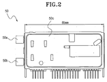
- Figure 2 shows the appearance of a conventional tuner block 50 that has the modulator 51, the tuner 53 and the IF/demodulator circuit 55 integrally formed therein.
- Figure 3 is a view showing a layout of an arrangement of a plurality of pins of the tuner block 50 shown in Figure 2.
- the twelve pins allocated to the tuner 53 comprise pin 6 (RF AGC) to control the gain amplifiers for received TV signals, pin 9 and pin 10 (SCL, SDA) connected to control buses to communicate with the CPU 30 through I 2 C communication, pin 13 (X-TAL IN) for receiving a clock signal.
- pins 7, 11 and 15 are not used.
- the arrangement of the pins according to the position of the modulator IC and the integrated tuner and the IF/demodulator circuit IC in the casing 50c, and signal interference problem must be considered, even in the case of manufacturing the tuner block using the IC in which the tuner and the IF/demodulator circuit are integrally formed. Therefore, to move some of the used pins to the positions of the unused pins (pin 7, 11, 15, 17, 18) to reduce the number of the pins complicates construction of the circuit that connects the modulator IC and the integrated tuner and IF/demodulator circuit IC in the casing 50c and increases a probability that noise caused by the signal interference will be generated.
- pin 16 is a reserved pin in both the conventional tuner block 50 and the tuner block 150. Where the reserved pin is also removed, the total number of the pins becomes fifteen.
- pins 1 through 6, pins 8 through 10, and pin 14 is the same as the arrangement of pins 1 through 6, pins 8 through 10, and pin 14 of the conventional tuner block 50.
- pin 3 is used for supplying the electrical power to the modulator, but in the tuner block 150 according to the present invention, pin 3 is used for supplying the electrical power to both the modulator and the tuner.
Landscapes
- Engineering & Computer Science (AREA)
- Multimedia (AREA)
- Signal Processing (AREA)
- Structure Of Receivers (AREA)
- Two-Way Televisions, Distribution Of Moving Picture Or The Like (AREA)
- Channel Selection Circuits, Automatic Tuning Circuits (AREA)
Abstract
Description
- The present invention relates to a tuner block comprising a casing, housing a tuner, an IF/demodulator circuit and a modulator, and an array, e.g. a linear array, of pins including pins for providing power and signal connections to the tuner, the IF/demodulator circuit and the modulator.
- As shown in Figure 1, broadcast signal receiving apparatus, such as a VCRs, comprise an A/
V block 10 for processing a video signal and an audio signal, adeck 20 for recording and reproducing video and audio signals on recording media such as a magnetic tape, atuner block 50 for demodulating broadcast signals picked up by anantenna 60 and aCPU 30 which controls the broadcast signal receiving apparatus. Thetuner block 50 has atuner 53 for tuning to broadcast signals, an IF/demodulator circuit 55 for demodulating the tuned broadcast signal and amodulator 51 for modulating a carrier with the video signal and the audio signal to provide an RF signal for aTV 70. - Generally, the
modulator 51, thetuner 53, and the IF/demodulator circuit 55.are integrally built in a casing and such a device is called as an integral-type tuner block. Thetuner block 50 is mounted on a printed circuit board in the VCR. Thetuner block 50 is connected with other devices such as the A/V block 10 and theCPU 30 mounted on the printed circuit board. - Figure 2 shows the appearance of a
conventional tuner block 50 that has themodulator 51, thetuner 53 and the IF/demodulator circuit 55 integrally formed therein. Figure 3 is a view showing a layout of an arrangement of a plurality of pins of thetuner block 50 shown in Figure 2. - As shown in Figure 2, the
tuner block 50 has acasing 50c, encompassing themodulator 51, thetuner 53, and the IF/demodulator circuit 55, and anantenna input terminal 50a and anantenna output terminal 50b disposed outside thecasing 50c. Theantenna input terminal 50a is connected to theantenna 60 and the 809antenna output terminal 50b is connected to theTV 70. The length of thecasing 50c is standardized at 85mm from a consideration of the arrangement of the plurality of pins projecting from thecasing 50c. - As shown in Figure 3, twenty-two pins projecting from the
casing 50c. The 22 pins consist of five pins (pin 1 through pin 5) associated with themodulator 51, twelve pins (pin 6 throughpin 16 and pin 21) associated with thetuner 53, and five pins (pin 17 throughpin 20 and pin 22) associated with the IF/demodulator circuit 55. - The five pins allocated to the
modulator 51 comprisepin 1 and pin 5 (AUDIO IN, VIDEO IN) for receiving audio and video inputs respectively, pin 2 (CH/SW) to receive a channel selection signal, pin 3 (MB (5V)) to receive a supply of electrical power needed for themodulator 51, and pin 4 (CONTROL) to receive a control signal for mode conversion between a TV mode and a VCR mode. - The twelve pins allocated to the
tuner 53 comprise pin 6 (RF AGC) to control the gain amplifiers for received TV signals,pin 9 and pin 10 (SCL, SDA) connected to control buses to communicate with theCPU 30 through I2C communication, pin 13 (X-TAL IN) for receiving a clock signal. Among the twelve pins allocated to thetuner 53,pins - The five pins allocated to the IF/
demodulator circuit 55 comprisepin 19 and pin 22 (AUDIO OUT, VIDEO OUT) to output audio and a video signals respectively, pin 20 (SIF OUT) to output a sound sub-carrier. Among the pins allocated to the IF/demodulator circuit 55,pins - Such an arrangement of the pins is determined from a consideration of the positions of three ICs (integrated circuits) corresponding to the
modulator 51, thetuner 53, and the IF/demodulator circuit 55 disposed in thecasing 50c. In other words, the ICs, which correspond to themodulator 51, thetuner 53, and IF/demodulator circuit 55, are consecutively disposed from an point adjacent to theantenna input terminal 50a and theantenna output terminal 50b in thecasing 50c. Considering the positions of the ICs, the pins used by themodulator 51 are disposed near to theantenna input terminal 50a and theantenna output terminal 50b, the pins used by thetuner 53 are disposed at a next position, and the pins used by the IF/demodulator circuit 55 are disposed at a farthest place from theantenna input terminal 50a and theantenna output terminal 50b. - Moreover, the arrangement of the pins is determined by the need to avoid stray coupling and cross-talk. For example, where the video output pin and the audio output pin are closely disposed, the video output signal causes interference to the audio output signal. Therefore, the video output pin and the audio output pin are disposed respectively at
pin 22 andpin 19 so as to be spaced by more than a predetermined distance. - However, the size of the
conventional tuner block 50 becomes unnecessarily large since more pins are provided than are actually used. In other words, as described above,pins conventional tuner block 50 has pins that are not used and the size of thetuner block 50 is unnecessarily large. Consequently, it is difficult to realize a compact broadcasting signal receiving apparatus because of the unnecessarilylarge tuner block 50. - Recently, an IC having an integrally formed tuner and IF/demodulator circuit has been developed. Therefore, a tuner block having simpler construction may be manufactured by installing two ICs (a modulator IC and the integrated tuner and IF/demodulator circuit IC) in the casing. Accordingly, a small-sized tuner block may be created.
- However, the arrangement of the pins according to the position of the modulator IC and the integrated tuner and the IF/demodulator circuit IC in the
casing 50c, and signal interference problem must be considered, even in the case of manufacturing the tuner block using the IC in which the tuner and the IF/demodulator circuit are integrally formed. Therefore, to move some of the used pins to the positions of the unused pins (pin casing 50c and increases a probability that noise caused by the signal interference will be generated. - A tuner block according to the present invention is characterised in that one of said pins is a power supply pin for supplying power to the tuner and the modulator.
- Preferably, among the plurality of pins,
pins 1 to 5 are used by the modulator,pins 6 to 11 and 14 are used by the tuner andpins - There may be a
pin 15 which is unused. - Preferably, among the plurality of pins,
pin 3 is the power supply pin. - Preferably, among the plurality of pins, a
pin 7 is a clock input pin for receiving a clock signal for use in the modulator and the tuner. - Preferably, among the plurality of pins,
pin 1 is an audio input pin,pin 2 is a channel selection pin, pin 4 is a control pin for receiving a control signal for selecting between a TV mode and a VCR mode and pin 5 is a video input pin. - Preferably, among the plurality of pins,
pin 6 is an automatic gain control pin,pin 8 is an AS pin for a tuner selection signal,pin 9 an SCL pin,pin 10 is an SDA pin andpin 11 is an AFT pin andpin 14 is a TU-V pin. - Preferably, among the plurality of pins,
pin 12 is an audio output pin (AUDIO OUT),pin 13 is a sound sub-carrier output pin (SIF OUT) which outputs a sound sub-carrier, andpin 16 is a video output pin (VIDEO OUT). - A printed circuit board including terminal means for receiving either the pins of a first tuner block or a second tuner block and switching means for rerouting power supply and/or signal paths so as to correctly connect said paths to both of said tuner blocks as necessary, wherein the second tuner block is a tuner block according to present invention and the first tuner block has more pins than the second tuner block.
- Embodiments of the present invention will now be described, by way of example, with reference to Figures 4 to 6B of the accompanying drawings, in which:
- Figure 1 is a schematic block diagram showing a conventional broadcast signal receiving apparatus;
- Figure 2 shows the tuner block having an integrated modulator and IF/demodulator circuit of Figure 1;
- Figure 3 shows the layout of pins of the tuner block of Figure 2;
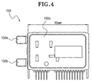
- Figure 4 shows a tuner block having an integrated modulator and IF/demodulator circuit according to the present invention;
- Figure 5 shows the layout of pins of the tuner block in Figure 4;
- Figure 6A shows a switching status of a printed circuit board adapted to accommodate either the tuner block of Figure 2 or the tuner block of Figure 4 and showing a switching status for operation of the tuner block of Figure 2; and
- Figure 6B shows the switching status of the printed circuit board shown in Figure 6A for operation of the tuner block of Figure 5.
- Referring to Figure 4, a
tuner block 150 comprises a modulator, tuner and IF/demodulator circuit and acasing 150c which accommodates the modulator, tuner and the IF/demodulator circuit. Anantenna input terminal 150a and anantenna output terminal 150b are installed outside thecasing 150c. A modulator IC is disposed at a position adjacent position to theantenna input terminal 150a and theantenna output terminal 150b in thecasing 150c. An integrated tuner and IF/demodulator circuit IC is disposed at a position remote from the modulator IC. - Sixteen pins are project from a side of the
casing 150c. The physical construction of each of the sixteen pins, such as size and shape of a pin, are the same as in theconventional tuner block 50 in Figure 2 and pitch of the pins is in theconventional tuner block 50. Thecasing 150c has a length of 60 to 65mm, which is smaller than theconventional tuner block 50, since the number of the pins is reduced compared to theconventional tuner block 50. Preferably, thetuner block 150 according to the present invention has the length of 65mm as shown in Figure 4. - Referring to Figure 5,
pin 1 and pin 5 (AUDIO IN, VIDEO IN) receive audio and video signals respectively from an audio/video block. Pin 2 (CH/SW) receives a channel selection signal (to select betweenchannels 3 and 4) which sets the output channel of the modulator. Pin 4 receives a control signal which selects between a TV mode and a VCR mode. - Pin 3 (+B (TU/MD)) supplies electrical power to the modulator and the tuner. Thus,
pin 1 through pin 5 are all used by the modulator. Among these pins,pin 3 is used for supplying the electrical power not only to the modulator but also to the tuner. To allowpin 3 to supply the electrical power to both the modulator and the tuner, the electrical power supply needs of the modulator IC and the integrated tuner and IF/demodulator circuit IC are commonly connected withpin 3 in thecasing 150c. - Pin 6 (RF AGC) receives a bias voltage to control the gain of the tuner. Pin 7 (X-TAL IN) receives a clock signal for use in the modulator and the tuner. Pin 8 (AS) receives a signal for setting the address of a tuner to be controlled where there is a plurality of tuners. Pin 9 (SCL) receives another clock signal used for communication with respect to a CPU using an I2C bus. Pin 10 (SDA) receives a command transmitted from the CPU through the I2C bus. Pin 11 (AFT) outputs a voltage, which is provided to the CPU for automatic fine tuning. Pin 12 (AUDIO OUT) outputs the audio signal. Pin 13 (SIF OUT) outputs a sound sub-carrier (4.5 MHz in the case of NTSC). Pin 14 (TU-V) outputs another voltage which is used by a local oscillator to produce the frequency required to tune a selected channel.
-
Pin 15 is a reserved pin, which is not used. Pin 16 (VIDEO OUT) outputs the video signal. - According to the above arrangement of the pins, pins 1 through 5 are used by the modulator, and pins 6 through 11 and 14 are used by the tuner.
Pins demodulator circuit 55, andpin 15 is not used.Pin 3 andpin 7 are used by both the modulator and the tuner. - According to the arrangement of the pins described above, six pins (
pin 17 through 22), which are used in theconventional tuner block 50, are eliminated and functions of the eliminated pins are included among the sixteen pins of thetuner block 150. Actually, the IF/demodulator circuit 55 of theconventional tuner block 50 uses only four pins (pins 19 through 22), thus among the pins (pin 1 through 16) allocated to themodulator 51 and thetuner 53 of theconventional tuner block 50, five pins are required to be reassigned to provide the interconnections previously provided bypins 19 through 22. Electrical power supply pin (pin 3) for the modulator and the electrical power supply pin (pin 12) for the tuner in theconventional tuner block 50 are integrated intopin 3 in thetuner block 150. Considering that the IF OUT pin (pin 16) in theconventional tuner block 50 is only used for testing, the IF OUT function has been removed and the VIDEO OUT function has been assigned to pin 16.Pin 15 is a reserved pin in both theconventional tuner block 50 and thetuner block 150. Where the reserved pin is also removed, the total number of the pins becomes fifteen. - In the
tuner block 150 according to the present invention, the arrangement of several pins is different from theconventional tuner block 50 as will be described in great detail below. - The arrangement of
pins 1 through 6, pins 8 through 10, andpin 14 is the same as the arrangement ofpins 1 through 6, pins 8 through 10, and pin 14 of theconventional tuner block 50. However, in theconventional tuner block 50,pin 3 is used for supplying the electrical power to the modulator, but in thetuner block 150 according to the present invention,pin 3 is used for supplying the electrical power to both the modulator and the tuner. - The clock input pin (X-TAL IN), which was
pin 13 in theconventional tuner block 50, has been moved topin 7, which was not used in theconventional tuner block 50. - The audio output pin (AUDIO OUT), which was
pin 19 in theconventional tuner block 50, has been moved to pin 12, which was used in theconventional tuner block 50 as power input for the tuner.Pin 12 of theconventional tuner block 50, as described above, has been integrated withpin 3. The video output (VIDEO OUT), which waspin 22 in theconventional tuner block 50, has been moved to pin ·16 which was used as IF OUT in theconventional tuner block 50. As described above, in thetuner block 150 of the present invention, the IF OUT function has been removed. - The sound sub-carrier signal (SIF OUT), which was
pin 20 in theconventional tuner block 50, has been moved to pin 13, which was used as the clock input signal (X-TAL IN) in theconventional tuner block 50. The AFT signal, which waspin 21 in theconventional tuner block 50, has been moved to pin 11, which was not used in theconventional tuner block 50. - According to the above construction, the electrical power needed for the tuner and the modulator is supplied through
pin 3, some of the previously reserved pins are used, the IF OUT function is eliminated, the number of the pins is reduced from 22 to 16, and one reserved pin is retained. - Since the audio output pin (AUDIO OUT) and the video output pin (VIDEO OUT) are respectively disposed at
pin 12 andpin 16, thepins conventional tuner block 50. Therefore, the influence of the video output signal on the audio output signal becomes less, and the audio signal will have a better quality. - In addition, according to the present invention, the audio output pin (AUDIO OUT) and the SIF OUT pin are adjacently disposed. The signals output from the audio output pin (AUDIO OUT) and the SIF OUT pin are input to an A/V block. Generally, there are two types of the A/V block. One is a mono model and the other is a hi-fi model having a hi-fi (high fidelity) IC. The hi-fi IC generates a final audio signal after a predetermined signal processing with regard to the output signal of the SIF OUT pin, and passes through the output signal of the AUDIO OUT pin. Therefore, in the case of a hi-fi model having a hi-fi IC, the audio output signal and the output signal at the SIF OUT pin are input to the A/V block. To this end, it is preferable that the audio output pin (AUDIO OUT) and the SIF OUT pin are adjacently disposed. Accordingly, a circuit construction on a printed circuit board, in which the
tuner block 150 and the A/V block are mounted, becomes simpler. - Since the SIF OUT pin and the clock input pin (X-TAL IN) are respectively disposed at
pin 13 andpin 7, the two pins are separated by six pins. Since the clock signal (X-TAL IN) and the sound sub-carrier (SIF OUT) are high frequency signals, where the SIF OUT pin and the clock input pin (X-TAL IN) are adjacently disposed to each other, the clock signal and the sound sub-carrier badly influence each other. Therefore, the SIF OUT pin and the clock input pin (X-TAL IN) are preferably disposed as far from each other as possible. In the present embodiment, the clock input (X-TAL IN) has been moved topin 7, which is the farthest pin from theSIF OUT pin 13 among the pins (7, 11, 15), which are not used in theconventional tuner block 50. Thus, although the SIF OUT pin and the clock input pin (X-TAL IN) are closer by 1 pin than in theconventional tuner block 50, an interval large enough to prevent interference being generated between the pins has been maintained, and the number of the pins required to be moved in order to interconnect thetuner block 150 is minimized - Furthermore, as described above, to maintain the interval between the SIF OUT pin and the clock input pin (X-TAL IN), and the interval between the audio output pin (AUDIO OUT) and the video output pin (VIDEO OUT), the SIF OUT pin is preferably disposed between the audio output pin (AUDIO OUT) and the video output pin (VIDEO OUT). In other words, in the present embodiment, the SIF OUT pin and the audio output pin (AUDIO OUT) are not disposed at
pin 12 andpin 13, respectively, but are disposed atpin 13 andpin 12, respectively. According to the above arrangement, the audio output pin (AUDIO OUT) and the video output pin (VIDEO OUT) are disposed to have the interval of four pins as described above, thus the AUDIO OUT pin and the VIDEO OUT pin are 1 pin further apart than in theconventional tuner block 50. Moreover, according to the above arrangement, also the SIF OUT pin and the clock input pin (X-TAL IN) are disposed to have the interval of six pins. - An automatic fine tuning pin (AFT) is used by the tuner. Thus, it is preferable that the automatic fine tuning pin (AFT) is disposed with other pins (
pin 6 through 10) which are also used by the tuner, thus, the AFT pin is disposed atpin 11. - Other pins excluding the pins moved as described above have been arranged as in the
conventional tuner block 50 to minimize the change of the position of the pins compared with theconventional tuner block 50. - Figures 6A and 6B show a switching circuit of the printed
circuit board 200, on which thetuner block 150 in Figure 5 is mounted. The switching circuit, shown in Figures 6A and 6B, is manufactured to accommodate either theconventional tuner block 50 as shown in Figure 6A, or atuner block 150 according to the present invention, as shown in Figure 6B, on the printedcircuit board 200. - As shown in Figures 6A and 6B, a clock signal input (X-TAL IN) line is connected with
pin 7 and pin 13 through afirst clock switch 211 and asecond clock switch 212. Where theconventional tuner block 50 is mounted on the printedcircuit board 200, thefirst clock switch 211 is off and thesecond clock switch 212 is on as shown in Figure 6A. Where thetuner block 150 of the present invention is mounted on the printedcircuit board 200, thefirst clock switch 211 is on and thesecond clock switch 212 is off as shown in Figure 6B. - An ATF output line is connected with
pin 21, and connected withpin 11 via anAFT switch 220. Where theconventional tuner block 50 is mounted on the printedcircuit board 200, theAFT switch 220 is off as shown in Figure 6A, and where thetuner block 150 according to the present invention is mounted on the printedcircuit board 200, theAFT switch 220 is on as shown in Figure 6B. - An SIF output line (SIF OUT) is connected with
pin 20 and connected withpin 13 via anSIF switch 240. Where theconventional tuner block 50 is mounted on the printedcircuit board 200, theSIF switch 240 is off as shown in Figure 6A, and where thetuner block 150 according to the present invention is mounted on the printedcircuit board 200, theSIF switch 240 is on as shown in Figure 6B. - A video signal output line (VIDEO OUT) is connected with
pin 22 and connected withpin 16 via avideo switch 250. Where theconventional tuner block 50 is mounted on the printedcircuit board 200, thevideo switch 250 is off as shown in Figure 6A, and where thetuner block 150 according to the present invention is mounted on the printedcircuit board 200, thevideo switch 250 is on as shown in Figure 6B. - An electrical power supply line (
Vcc 5V) is connected withpin 3, and an audio output (AUDIO OUT) line is connected withpin 19. The electrical power supply line (Vcc 5V) and the audio output (AUDIO OUT) line are connected withpin 12 through aconversion switch 230. Where theconventional tuner block 50 is mounted on the printedcircuit board 200, theconversion switch 230 is switched to connectpin 12 with the electrical power (Vcc 5V) as shown in Figure 6A, and where thetuner block 150 according to the present invention is mounted on the printedcircuit board 200, theconversion switch 230 is switched to connectpin 12 with the audio output (AUDIO OUT) line as shown in Figure 6B. Therefore, where theconventional tuner block 50 is mounted, the electrical power is supplied to the modulator throughpin 12, and where thetuner block 150 according to the present invention is mounted, the audio signal output throughpin 12 is transmitted to the A/V block. - Each of the
switches circuit board 200. In other words, by changing the installation position of the jumper installed on the printedcircuit board 200, the electrical connection status between the parts mounted on the printedcircuit board 200 is changed. Therefore, without changing the arrangement of holes which are formed on the printedcircuit board 200 for mounting the tuner block, the electrical connection status of the printedcircuit board 200 is changeable to be used with either theconventional tuner block 50 or thetuner block 150 according to the present invention. - One way of changing the electrical connection status is to change a jumper installation program of a chip mounting apparatus. Another way of changing the electrical connection status is to manufacture the printed
circuit board 200 to include theswitches conventional tuner block 50 and thetuner block 150 according to the present invention. Consequently, thetuner block 150 may be used interchangeably with the conventional tuner block by appropriately setting theswitches - Since the electrical power for supplying the electrical power to the modulator and the tuner is provided by a common pin (pin 3) in the
tuner block 150, the number of the pins is reduced, and a small-sized tuner block compared to the conventional tuner block may be manufactured. - Moreover, each pin of the
tuner bock 150 is disposed to correspond to the position of the modulator IC and the integrated tuner and IF/ demodulator circuit IC disposed in the casing, thus the tuner block is compact, and at the same time, the circuit construction in the casing is simplified. In addition, the noise and interference between the signals in thetuner block 150 is minimized. - Furthermore, by changing installation positions of jumpers in the printed circuit board, one of the conventional tuner block and the tuner block according to the present invention is selectively installable. Compared with the
conventional tuner block 50, the number of the pins changed to result in thetuner block 150 is minimized, thus the number of jumpers which are changed in position is reduced.
Claims (3)
- An interface circuit for selectively using one of a first tuner block having a first predetermined number of connector pins and a second tuner block having a second predetermined number of connector pins, wherein a third predetermined number of corresponding pins of the first and second predetermined numbers of pins have different functional assignments, the interface circuit comprising:a first switch which connects a first of the corresponding pins to a power supply input voltage to selectively use the first tuner block or connects the first corresponding pin to an audio output function to selectively use the second tuner block;a second switch which disconnects a clock input signal from a second of the corresponding pins to selectively use the first tuner block and connects the clock input signal to the second corresponding pin to selectively use the second tuner block;a third switch which connects the clock input signal to a third of the corresponding pins to selectively use the first tuner block and disconnects the clock input signal from the third corresponding pin to selectively use the second tuner block;a fourth switch which connects the third corresponding pin to a sound sub-carrier output to selectively use the second tuner block and disconnects the third corresponding pin from the sound sub-carrier output to selective use the first tuner block;a fifth switch which disconnects an automatic fine tuning output from a fourth of the corresponding pins to selectively use the first tuner block and connects the fourth corresponding pin to the automatic fine tuning output to selectively use the second tuner block; anda sixth switch which connects a video output to a fifth of the corresponding pins to selectively use the second tuner block and disconnects the fifth corresponding pin from the video output to selectively use the first tuner block.
- An interface circuit for selectively using one of a first tuner block having a first predetermined number of connector pins and a second tuner block having a second predetermined number of connector pins, wherein a third predetermined number of corresponding pins of the first and second predetermined numbers of pins have different functional assignments, the interface circuit comprising:a circuit board having a plurality of circuit paths, each circuit path connecting a respective pin of the third predetermined number of corresponding pins with additional circuitry, each of the plurality of circuits path having an opening in the circuit path adapted to receive a jumper;a first jumper which completes a first of the plurality of circuit paths to connect a first of the corresponding pins to a power,supply input to selectively use the first tuner block or completes a second of the plurality of circuit paths to connect the first corresponding pin to an audio output to selectively use the second tuner block; anda second jumper which completes a third of the plurality of circuit paths to connect a clock input to a second of the corresponding pins to selectively use the second tuner block or completes a fourth of the plurality of circuit paths to connect the clock input to a third of the corresponding pins to selectively use the first tuner block.
- The interface circuit according to claim 24, further comprising:a third jumper which completes a fifth of the plurality of circuit paths to connect the third corresponding pin to a sound sub-carrier output to selectively use the second tuner block;a fourth jumper which completes a sixth of the plurality of circuit paths to connect a fourth of the corresponding pins to an automatic fine tuning output to selectively use the second tuner block; anda fifth jumper which completes a seventh of the plurality of circuit paths to connect a video output to a fifth of the corresponding pins to selectively use the second tuner block.
Applications Claiming Priority (3)
| Application Number | Priority Date | Filing Date | Title |
|---|---|---|---|
| KR1020010062462A KR100395562B1 (en) | 2001-10-10 | 2001-10-10 | Tuner block for use in a video signal receiving apparatus, having a modulator, a tuner and IF/demodulator circuit in a casing |
| KR2001062462 | 2001-10-10 | ||
| EP02252972A EP1303137A3 (en) | 2001-10-10 | 2002-04-26 | Television tuner |
Related Parent Applications (2)
| Application Number | Title | Priority Date | Filing Date |
|---|---|---|---|
| EP02252972.1 Division | 2002-04-26 | ||
| EP02252972A Division EP1303137A3 (en) | 2001-10-10 | 2002-04-26 | Television tuner |
Publications (2)
| Publication Number | Publication Date |
|---|---|
| EP1404131A1 true EP1404131A1 (en) | 2004-03-31 |
| EP1404131B1 EP1404131B1 (en) | 2005-07-20 |
Family
ID=36089225
Family Applications (2)
| Application Number | Title | Priority Date | Filing Date |
|---|---|---|---|
| EP03028456A Expired - Lifetime EP1404131B1 (en) | 2001-10-10 | 2002-04-26 | Interface circuit for television tuner |
| EP02252972A Ceased EP1303137A3 (en) | 2001-10-10 | 2002-04-26 | Television tuner |
Family Applications After (1)
| Application Number | Title | Priority Date | Filing Date |
|---|---|---|---|
| EP02252972A Ceased EP1303137A3 (en) | 2001-10-10 | 2002-04-26 | Television tuner |
Country Status (6)
| Country | Link |
|---|---|
| US (2) | US6947722B2 (en) |
| EP (2) | EP1404131B1 (en) |
| KR (1) | KR100395562B1 (en) |
| CN (1) | CN1233116C (en) |
| DE (1) | DE60205115T2 (en) |
| MY (1) | MY128085A (en) |
Families Citing this family (7)
| Publication number | Priority date | Publication date | Assignee | Title |
|---|---|---|---|---|
| KR100395562B1 (en) * | 2001-10-10 | 2003-08-21 | 삼성전자주식회사 | Tuner block for use in a video signal receiving apparatus, having a modulator, a tuner and IF/demodulator circuit in a casing |
| US7046166B2 (en) * | 2003-04-29 | 2006-05-16 | Rockwell Scientific Licensing, Llc | Modular wireless integrated network sensor (WINS) node with a dual bus architecture |
| JP2005102151A (en) * | 2003-08-27 | 2005-04-14 | Sony Corp | Digital broadcast receiver tuner |
| JP2007267172A (en) * | 2006-03-29 | 2007-10-11 | Alps Electric Co Ltd | Tuner for digital broadcasting, and digital broadcast receiving apparatus using same |
| US8316402B2 (en) * | 2008-01-16 | 2012-11-20 | Verint Systems Inc. | System for selecting a video or audio path |
| TW200934242A (en) * | 2008-01-21 | 2009-08-01 | Delta Electronics Inc | Projection apparatus and signal converting module thereof |
| US20170171593A1 (en) * | 2015-12-14 | 2017-06-15 | Le Holdings (Beijing) Co., Ltd. | Tuner unit module, tuner and electronic device |
Citations (1)
| Publication number | Priority date | Publication date | Assignee | Title |
|---|---|---|---|---|
| EP0484051A2 (en) * | 1990-10-31 | 1992-05-06 | Raytheon Company | Telephone interface circuit |
Family Cites Families (17)
| Publication number | Priority date | Publication date | Assignee | Title |
|---|---|---|---|---|
| US4509210A (en) * | 1981-11-30 | 1985-04-02 | Rca Corporation | Television receiver adaptable for descrambler module |
| US5508815A (en) * | 1981-12-14 | 1996-04-16 | Smart Vcr Limited Partnership | Schedule display system for video recorder programming |
| CA1212457A (en) * | 1983-06-14 | 1986-10-07 | Nec Kansai, Ltd. | Frequency converter, especially catv converter |
| JPS61150410A (en) * | 1984-12-24 | 1986-07-09 | Sony Corp | Tuner device |
| JPH0346827A (en) * | 1989-07-14 | 1991-02-28 | Matsushita Electric Ind Co Ltd | Television tuner |
| JP2559005B2 (en) * | 1993-01-07 | 1996-11-27 | 松下電器産業株式会社 | Double super tuner |
| JP2663823B2 (en) * | 1993-01-29 | 1997-10-15 | 松下電器産業株式会社 | High frequency device |
| JP2661499B2 (en) * | 1993-03-08 | 1997-10-08 | 関西日本電気株式会社 | Tuner unit |
| JP3533033B2 (en) * | 1996-04-10 | 2004-05-31 | 松下電器産業株式会社 | High frequency device |
| KR100269159B1 (en) * | 1998-09-05 | 2000-10-16 | 윤종용 | Tuner Circuit Design Method |
| CN2369420Y (en) | 1998-12-30 | 2000-03-15 | 厦门科华俐发展有限公司 | Wire audio frequency receiver |
| KR100286813B1 (en) * | 1999-03-23 | 2001-04-16 | 이형도 | Digital bs tuner |
| JP3870003B2 (en) * | 1999-12-15 | 2007-01-17 | アルプス電気株式会社 | High frequency unit for VTR |
| KR100311830B1 (en) * | 2000-02-21 | 2001-10-17 | 이형도 | Channel moduel apparatus for set-top box |
| US6404309B1 (en) * | 2000-06-09 | 2002-06-11 | Thomson Licensing, S.A. | Tuner with non-edge RF input pin/lead |
| JP3729254B2 (en) * | 2001-10-02 | 2005-12-21 | アルプス電気株式会社 | Video equipment tuner mounting board |
| KR100395562B1 (en) * | 2001-10-10 | 2003-08-21 | 삼성전자주식회사 | Tuner block for use in a video signal receiving apparatus, having a modulator, a tuner and IF/demodulator circuit in a casing |
-
2001
- 2001-10-10 KR KR1020010062462A patent/KR100395562B1/en not_active Expired - Fee Related
-
2002
- 2002-01-15 US US10/045,043 patent/US6947722B2/en not_active Expired - Fee Related
- 2002-04-19 MY MYPI20021447A patent/MY128085A/en unknown
- 2002-04-26 DE DE60205115T patent/DE60205115T2/en not_active Expired - Fee Related
- 2002-04-26 EP EP03028456A patent/EP1404131B1/en not_active Expired - Lifetime
- 2002-04-26 EP EP02252972A patent/EP1303137A3/en not_active Ceased
- 2002-05-23 CN CNB021204144A patent/CN1233116C/en not_active Expired - Fee Related
-
2005
- 2005-08-12 US US11/202,071 patent/US7489917B2/en not_active Expired - Fee Related
Patent Citations (1)
| Publication number | Priority date | Publication date | Assignee | Title |
|---|---|---|---|---|
| EP0484051A2 (en) * | 1990-10-31 | 1992-05-06 | Raytheon Company | Telephone interface circuit |
Also Published As
| Publication number | Publication date |
|---|---|
| EP1303137A2 (en) | 2003-04-16 |
| US7489917B2 (en) | 2009-02-10 |
| DE60205115T2 (en) | 2006-04-13 |
| MY128085A (en) | 2007-01-31 |
| EP1404131B1 (en) | 2005-07-20 |
| KR100395562B1 (en) | 2003-08-21 |
| CN1411176A (en) | 2003-04-16 |
| KR20030029761A (en) | 2003-04-16 |
| US6947722B2 (en) | 2005-09-20 |
| CN1233116C (en) | 2005-12-21 |
| DE60205115D1 (en) | 2005-08-25 |
| EP1303137A3 (en) | 2003-05-14 |
| US20030068992A1 (en) | 2003-04-10 |
| US20050266812A1 (en) | 2005-12-01 |
Similar Documents
| Publication | Publication Date | Title |
|---|---|---|
| EP1404131B1 (en) | Interface circuit for television tuner | |
| US7293998B2 (en) | Electronic device and circuit module device | |
| WO2002071747A1 (en) | Interface module for a tv set | |
| KR100278398B1 (en) | Video apparatus | |
| US7174140B2 (en) | RF system integrated with RF switch and RF modulation | |
| US20110111712A1 (en) | Broadcasting receiver | |
| EP0899877A1 (en) | IC for tuner | |
| KR20030010665A (en) | Apparatus for providing tuner parameters in a television receiver | |
| KR20070048751A (en) | RF selection switch circuit, tuning system and RF signal receiver | |
| US20070002176A1 (en) | Intelligent network interface module | |
| US20250211812A1 (en) | Global intergraded tuner apparatus and method for controlling the same | |
| KR100221476B1 (en) | Integrated ICIC bus transmission method of TV | |
| US20050042900A1 (en) | Cable modem module unit and electronic unit | |
| KR100532776B1 (en) | TV/FM Radio Combination Receiving Equipment For AVN System | |
| KR20000048447A (en) | Television circuit designed to receive or transmit signals from or in different directions | |
| JPH09214373A (en) | Electronic equipment unit | |
| KR100577709B1 (en) | Digital broadcasting signal receiving unit | |
| KR20210117640A (en) | Tuner Circuit Board | |
| KR100406354B1 (en) | Input switching circuit with function of loop through in tuner | |
| KR20050090238A (en) | Combination system | |
| JPH07312564A (en) | Tuner device | |
| KR19980049120U (en) | VSI System with Line Jack | |
| JP2001326536A (en) | Audio equipment | |
| JPS63283290A (en) | Catv converter |
Legal Events
| Date | Code | Title | Description |
|---|---|---|---|
| PUAI | Public reference made under article 153(3) epc to a published international application that has entered the european phase |
Free format text: ORIGINAL CODE: 0009012 |
|
| AC | Divisional application: reference to earlier application |
Ref document number: 1303137 Country of ref document: EP Kind code of ref document: P |
|
| AK | Designated contracting states |
Kind code of ref document: A1 Designated state(s): AT BE CH CY DE DK ES FI FR GB GR IE IT LI LU MC NL PT SE TR |
|
| AX | Request for extension of the european patent |
Extension state: AL LT LV MK |
|
| 17P | Request for examination filed |
Effective date: 20040510 |
|
| 17Q | First examination report despatched |
Effective date: 20040719 |
|
| AKX | Designation fees paid |
Designated state(s): DE FR GB NL |
|
| GRAP | Despatch of communication of intention to grant a patent |
Free format text: ORIGINAL CODE: EPIDOSNIGR1 |
|
| RAP1 | Party data changed (applicant data changed or rights of an application transferred) |
Owner name: SAMSUNG ELECTRONICS CO., LTD. |
|
| GRAS | Grant fee paid |
Free format text: ORIGINAL CODE: EPIDOSNIGR3 |
|
| GRAA | (expected) grant |
Free format text: ORIGINAL CODE: 0009210 |
|
| AC | Divisional application: reference to earlier application |
Ref document number: 1303137 Country of ref document: EP Kind code of ref document: P |
|
| AK | Designated contracting states |
Kind code of ref document: B1 Designated state(s): DE FR GB NL |
|
| REG | Reference to a national code |
Ref country code: GB Ref legal event code: FG4D |
|
| REF | Corresponds to: |
Ref document number: 60205115 Country of ref document: DE Date of ref document: 20050825 Kind code of ref document: P |
|
| ET | Fr: translation filed | ||
| PLBE | No opposition filed within time limit |
Free format text: ORIGINAL CODE: 0009261 |
|
| STAA | Information on the status of an ep patent application or granted ep patent |
Free format text: STATUS: NO OPPOSITION FILED WITHIN TIME LIMIT |
|
| 26N | No opposition filed |
Effective date: 20060421 |
|
| PGFP | Annual fee paid to national office [announced via postgrant information from national office to epo] |
Ref country code: DE Payment date: 20080502 Year of fee payment: 7 Ref country code: FR Payment date: 20080312 Year of fee payment: 7 |
|
| PGFP | Annual fee paid to national office [announced via postgrant information from national office to epo] |
Ref country code: NL Payment date: 20080403 Year of fee payment: 7 |
|
| PGFP | Annual fee paid to national office [announced via postgrant information from national office to epo] |
Ref country code: GB Payment date: 20080430 Year of fee payment: 7 |
|
| GBPC | Gb: european patent ceased through non-payment of renewal fee |
Effective date: 20090426 |
|
| NLV4 | Nl: lapsed or anulled due to non-payment of the annual fee |
Effective date: 20091101 |
|
| REG | Reference to a national code |
Ref country code: FR Ref legal event code: ST Effective date: 20091231 |
|
| PG25 | Lapsed in a contracting state [announced via postgrant information from national office to epo] |
Ref country code: DE Free format text: LAPSE BECAUSE OF NON-PAYMENT OF DUE FEES Effective date: 20091103 |
|
| PG25 | Lapsed in a contracting state [announced via postgrant information from national office to epo] |
Ref country code: NL Free format text: LAPSE BECAUSE OF NON-PAYMENT OF DUE FEES Effective date: 20091101 |
|
| PG25 | Lapsed in a contracting state [announced via postgrant information from national office to epo] |
Ref country code: FR Free format text: LAPSE BECAUSE OF NON-PAYMENT OF DUE FEES Effective date: 20091222 Ref country code: GB Free format text: LAPSE BECAUSE OF NON-PAYMENT OF DUE FEES Effective date: 20090426 |