EP1402700B1 - Adaptive predistorter based on the probability distribution function of the output amplitude - Google Patents
Adaptive predistorter based on the probability distribution function of the output amplitude Download PDFInfo
- Publication number
- EP1402700B1 EP1402700B1 EP03709499A EP03709499A EP1402700B1 EP 1402700 B1 EP1402700 B1 EP 1402700B1 EP 03709499 A EP03709499 A EP 03709499A EP 03709499 A EP03709499 A EP 03709499A EP 1402700 B1 EP1402700 B1 EP 1402700B1
- Authority
- EP
- European Patent Office
- Prior art keywords
- circuit
- input signal
- output
- phase
- output signal
- Prior art date
- Legal status (The legal status is an assumption and is not a legal conclusion. Google has not performed a legal analysis and makes no representation as to the accuracy of the status listed.)
- Expired - Lifetime
Links
Images


Classifications
-
- H—ELECTRICITY
- H04—ELECTRIC COMMUNICATION TECHNIQUE
- H04L—TRANSMISSION OF DIGITAL INFORMATION, e.g. TELEGRAPHIC COMMUNICATION
- H04L27/00—Modulated-carrier systems
- H04L27/32—Carrier systems characterised by combinations of two or more of the types covered by groups H04L27/02, H04L27/10, H04L27/18 or H04L27/26
- H04L27/34—Amplitude- and phase-modulated carrier systems, e.g. quadrature-amplitude modulated carrier systems
- H04L27/36—Modulator circuits; Transmitter circuits
- H04L27/366—Arrangements for compensating undesirable properties of the transmission path between the modulator and the demodulator
- H04L27/367—Arrangements for compensating undesirable properties of the transmission path between the modulator and the demodulator using predistortion
- H04L27/368—Arrangements for compensating undesirable properties of the transmission path between the modulator and the demodulator using predistortion adaptive predistortion
-
- H—ELECTRICITY
- H03—ELECTRONIC CIRCUITRY
- H03F—AMPLIFIERS
- H03F1/00—Details of amplifiers with only discharge tubes, only semiconductor devices or only unspecified devices as amplifying elements
- H03F1/32—Modifications of amplifiers to reduce non-linear distortion
- H03F1/3241—Modifications of amplifiers to reduce non-linear distortion using predistortion circuits
- H03F1/3247—Modifications of amplifiers to reduce non-linear distortion using predistortion circuits using feedback acting on predistortion circuits
-
- H—ELECTRICITY
- H03—ELECTRONIC CIRCUITRY
- H03F—AMPLIFIERS
- H03F1/00—Details of amplifiers with only discharge tubes, only semiconductor devices or only unspecified devices as amplifying elements
- H03F1/32—Modifications of amplifiers to reduce non-linear distortion
- H03F1/3241—Modifications of amplifiers to reduce non-linear distortion using predistortion circuits
- H03F1/3294—Acting on the real and imaginary components of the input signal
-
- H—ELECTRICITY
- H03—ELECTRONIC CIRCUITRY
- H03F—AMPLIFIERS
- H03F2200/00—Indexing scheme relating to amplifiers
- H03F2200/102—A non-specified detector of a signal envelope being used in an amplifying circuit
Definitions
- the invention relates to the area of non-linear circuits and more specifically to the area of compensating for non-linearities introduced into signals by signal processing circuits.
- an input signal is provided to a transmitter for transmission therefrom.
- the transmitter conditions the signal so that it is in a form suitable for transmission.
- Such conditioning typically involves power amplification, where it is desirable to operate power amplifiers (PAs) near saturation in order to attain high power efficiency.
- PAs power amplifiers
- Unfortunately, such operation typically introduces non-linear distortion in the amplified signal. This is evidenced by spectrum re-growth, which diverts some of the energy from a desired frequency channel into adjacent frequency channels. This results in a loss of performance within a desired frequency channel as well as the creation of interference within adjacent frequency channels.
- analog linearization circuits are often used in conjunction with PAs and are manually tuned for each PA in an attempt to provide optimum performance. In general, this is costly but considered necessary for space applications where total available power for signal transmission is very limited.
- ground terminal use the use of a linearization circuit is typically not implemented due to its cost. Instead, a more powerful PA is utilized and operated in an input back-off mode of operation - with a reduced output power level. The reduction in power amplifier output capability is typically a less costly implementation than the use of a linearization circuit.
- the output power capability of PA's is currently very limited and thus a more efficient use of the available power would significantly reduce the cost. In some cases, about 70% of the cost of 30/20 GHz satellite terminal is in the RF front end, with approximately half of this cost associated with the PA.
- the prior art is limited in that spectrum efficient modulation, such as a multilevel quadrature amplitude modulation, or pulse shaping filters with a small roll-off factor, resulting in a significant envelope variation, often cannot be used due to the need to operate the PA within its linear region. Thus, efficiency of the PA is reduced. Additional limitations found in the prior art are a need to down-convert and demodulate the PA output signal, the comparing of the input signal to the reconstructed signal from the output port of the PA, a need to interrupt signal transmission, or they are limited to non-transmit periods of time, which is suitable for TDMA systems but not to FDMA systems.
- a method of compensating for non-linear conversion distortions of a circuit having an input signal provided thereto comprising the steps of: (a) determining a result of a statistical function of the input signal; (b) transforming the input signal in a non-linear manner to form an output signal; (c) sampling a portion of the output signal to provide a set of output samples each sampled at a different time, wherein a sample comprises at least one of an amplitude value and a phase value; (d) determining a result of a same statistical function of the output signal based on the set of output samples; (e) deriving predistortion information based on the result of the statistical function of the input signal and the result of the statistical function of the output signal; and (f) wherein the statistical function is one of a cumulative distribution function and a probability density function.
- the non-linear conversion distortion is a result of at least one of AM-AM conversion by the non-linear circuit and AM-PM conversion by the non-linear circuit.
- the method comprises the step of (g) updating the predistortion information in dependence upon the statistical function of the output signal having changed as a result of a change in the step of transforming.
- the circuit has at least one of a monotonic and continuous relationship between an amplitude of the input signal and an amplitude of the output signal up to a predetermined output signal level of the circuit and a continuous relationship between a phase of the input signal and a phase of the output signal up to a predetermined output signal level of the circuit.
- the step of deriving comprises the steps of: determining a plurality of data values, each data value for mapping a data point along the statistical function of the output signal to a data point along the statistical function of the input signal; and, storing the data values.
- the step of deriving comprises the steps of: determining a conditional histogram of a linear circuit output phase for a predetermined input signal amplitude; determining a conditional histogram of a non-linear circuit output phase for a predetermined input signal amplitude; and using the two determined conditional histograms to derive phase shift information for AM-PM conversion for forming a portion of the predistortion information.
- a circuit comprising: a memory circuit for storing a result of a statistical function of an input signal being provided to the circuit; a transforming circuit for transforming the input signal in a non-linear manner to form an output signal; a sampling circuit for sampling a portion of the output signal to provide a set of output samples each sampled at a different time, wherein a sample comprises at least one of an amplitude value and a phase value; a processor for determining a result of a same statistical function of the output signal based on the set of output samples and for deriving predistortion informatiom based on the result of the statistical function of the input signal and the result of the same statistical function of the output signal; and a predistortion circuit for predistorting the input signal being provided to the circuit in dependence upon the predistortion information, wherein the statistical function is one of a cumulative distribution function and a probability density function.
- FIG. 1 a illustrates a typical RF transmitter circuit having a predistortion circuit that is used to perform AM-AM compensation for non-linear conversion effects of a non-linear circuit, in the form of a power amplifier circuit;
- FIG. 14b illustrates a typical RF transmitter circuit having a predistortion circuit that is used to perform AM-AM and/or AM-PM compensation for non-linear conversion effects of a non-linear circuit, in the form of a power amplifier circuit;
- FIG. 2a illustrates a graph of normalized input signal amplitude vs. normalized output signal amplitude
- FIG. 2b illustrates a graph of normalized input signal amplitude vs. output signal phase shift in degrees
- FIG. 3 illustrates a block diagram of a topical transmitter apparatus absent a predistortion circuit
- FIG. 4 illustrates a graph of the CDF vs. normalized input signal amplitude
- FIG. 5 illustrates the mapping to restore a corresponding value of the PA output CDF to that of a reference CDF
- FIG. 6 illustrates a graph showing normalized output signal amplitude vs. normalized input signal amplitude
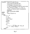
- FIG. 7 illustrates a process for determination of predistortion function for predistorting the input signal of the PA
- FIGs. 8a and 8b illustrate examples of 2-dimensional histograms from a 16-QAM modulated transmission system used with a SQRC pulse-shaping filter of a linear amplifier output phase and a nonlinear amplifier output phase, respectively;
- FIG. 9a illustrates contours representing the result of the linear amplification in terms of normalized PA input signal amplitude vs, the PA output signal phase
- FIG. 9b illustrates contours representing the result of the nonlinear amplification in terms of the normalized PA input signal amplitude vs. the PA output signal phase;
- FIG. 10 illustrates a phase shift difference between a reference conditional histogram and a PA output conditional histogram
- FIG. 11 illustrate a graph of PA output signal phase shift vs. normalized input signal amplitude, having plotted thereon a first set of data representing an actual AM-PM conversion and a second set of data representing an estimated AM-PM conversion;
- FIG. 12 illustrates a graph of the output signal phase shift wiz normalized input signal amplitude, where the phase response of the predistorter, the PA phase response and the total combined predistorter phase response and PA phase response are plotted;
- FIG. 13 illustrates a process, in accordance with another embodiment of the invention, that is used to calculate the phase predistortion from the histograms of the PA output signal phase;
- FIG. 14a illustrates another embodiment of the invention, a transmitter circuit employing a predistortion circuit and a complex envelope detector circuit for compensating for AM-AM and/or AM-PM signal distortion;
- FIG. 14b illustrates another embodiment of the invention, a transmitter circuit employing a predistortion circuit and a power detector circuit for compensating for AM-AM signal distortion;
- FIG. 14c illustrates another embodiment of the invention, a direct transmitter circuit employing a quadrature demodulator circuit
- FIG. 14d illustrates operational steps used in the operating of transmitter circuits illustrated in FIGs. 14a, 14b and 14c ;
- FIG. 15 illustrates an OFDM signal spectrum before and after predistortion compensation
- FIG. 16a illustrates received I-Q constellation for a single frequency channel before compensation for PA non-linearities
- FIG. 16b illustrates received I-Q constellation for a single frequency channel after compensation for PA non-linearities
- FIG. 17a illustrates a transmitted frequency spectrum for a 16-QAM channel without predistortion of the input signal to the PA
- FIG. 17b illustrates a transmitted frequency spectrum for a 16-QAM channel where predistortion is provided to the input signal prior to being amplified by the PA;
- FIG. 18a illustrates received I-Q constellation without using the predistorter
- FIG. 18b illustrates received I-Q constellation when used with the predistorter.
- FIGs. 1a and 1b each illustrate a typical transmitter circuit 100 having a predistortion circuit 101 that is used to compensate for non-linear conversion effects of a non-linear circuit, in the form of a power amplifier circuit (PA) 102.
- An input signal in the form of a bit stream is provided to an input port 100a for being received by a mapping circuit 103, having a signal generator disposed therein, used to generate an in-phase (I) symbol at a first output port 103a and a quadrature (Q) symbol at a second output port 103b thereof.
- Pulse shaping circuits 104a and 104b are connected to output ports 103a and 103b, respectively, for receiving the I and Q symbols and for pulse shaping thereof.
- the I and Q pulse shaped signals are provided to the predistortion circuit 101 for predistortion thereof.
- each signal is converted from a digital domain to an analog domain using digital to analog (DA) converters (DACs) 105a and 105b.
- DACs digital to analog converters
- DACs digital to analog converters
- a modulator circuit 106 receives the DA converted signals.
- the modulated signal is provided to the power amplifier circuit 102, in the form of either a solid state power amplifier circuit (SSPA) or another type of non-linear amplifier circuit.
- Predistortion information for being provided to the predistortion circuit 101 is derived from an output signal of the PA 102 using an envelope detector circuit 107 connected to an output port 100b of the PA 102.
- a circuit that provides an output signal that has amplitude that is not linearly related to the input signal amplitude exhibits AM-AM distortion.
- a power detector circuit 112 is used to recover the output signal envelope ampliltude. If AM-PM distortion compensation is potentially sought in addition to AM-AM, a complex envelope detector circuit (CED) 107 ( FIG. 1b ) that provides envelope phase and amplitude information is utilized.
- a power detector 112 FIG. 1a
- a CED 107 FIG. 1b
- two LPF's, two OpAmps and potentially two ADC's are utilized.
- the CED 107 output signals are provided to anti-aliasing filters (LPF) 108a and 108b and, optionally, operational amplifiers (OpAmps) 109a and 109b followed by potentially two analog-to-digital converters (ADC) 110a and 110b and a digital signal processor (DSP) 111.
- LPF anti-aliasing filters
- OpAmps operational amplifiers
- ADC analog-to-digital converters
- DSP digital signal processor
- a power detector circuit 112 output signal is provided to a single anti-aliasing filter 108, optionally an operational amplifier 109, and a single ADC 110.
- the DSP 111 provides predistortion coefficients to the predistortion circuit 101 for predistortion of the pulse shaped I and Q signals, thus closing a feedback path from the output port 100b.
- Equations (1) and (2) ⁇ ( t ) is the amplitude of the input signal and ⁇ ( t ) is the phase of the input signal.
- G ( ⁇ ( t )) is the amplitude response of the PA, otherwise known as AM-AM conversion, and ⁇ ( ⁇ ( t )) is the phase response, otherwise known as AM-PM conversion, of the PA.
- G ( ⁇ ( t )) and ⁇ ( ⁇ ( t )) are expressed as: G a t ⁇ ⁇ o ⁇ ⁇ ⁇ a t ⁇ a t ⁇ ⁇ ⁇ ⁇ ⁇ ⁇ ⁇
- the gain and phase response of the PA are separable.
- the gain response and the phase response are treated separately, thereby simplifying the process of PA non-linear distortion compensation.
- FIG. 2a illustrates a graph of normalized input signal amplitude vs. normalized output signal amplitude.
- the graph has a first set of data points that represents the measured amplitude response 201 of the PA along with a plot of a continuous function representing the least-squares fit equation 202 for the first set of data points.
- FIG. 2b illustrates a graph of normalized input signal amplitude vs. output signal phase shift in degrees.
- the graph has a first set of data points representing a measured phase response 203 of the PA along with a plot of a continuous least-squares fit equation 204 for ⁇ ( ⁇ ( t )).
- FIGs. 2a and 2b illustrate a close match between the modeled and measured amplitude and phase responses of the PA.
- Type is a term used in information theory for a histogram estimate of a discrete probability density function as is found in the text of T. Cover and J. Thomas, Elements of information theory, John Wiley & Sons, Inc., New York, 1991, pp.279-335 .
- Type information describes the statistical property of a time series, where cumulative distribution function (CDF) and probability density function (PDF) are examples thereof.
- CDF cumulative distribution function
- PDF probability density function
- AM-AM conversion and AM-PM conversion are considered separately for the PA due to their separability.
- ⁇ ( ⁇ ( t )) 0 is assumed without loss of generality.
- FIG. 3 illustrates a block diagram of a typical transmitter apparatus 300, absent a predistortion circuit, in which an input signal, in the form of an input bit stream, is provided to an input port 300a of a mapping circuit 303 for being split into two symbol streams.
- One symbol stream is termed the in-phase (I) component, and the other the quadrature (Q) component.
- Two pulse-shaping filters 304a and 304b are used to pulse-shape the I and Q components before they are modulated onto a carrier signal by a modulator circuit 306 that includes a frequency up-conversion circuit used to convert the signal to a predetermined transmission frequency for transmission.
- the PA 302 amplifies the modulated carrier signal before transmission from an output port 300b of the typical transmitter apparatus.
- Two commonly used pulse-shaping filters 304a and 304b are square-root raised-cosine (SQRC) filters and Gaussian filters.
- SQLRC square-root raised-cosine
- the signal After modulation, the signal is provided to the PA 302 and thus a pulse-shaped and carrier-modulated signal results, where the envelope of this signal encodes specific type information.
- the AM-AM conversion of the PA 302 distorts the input type information and more specifically the input signal envelope amplitude.
- a predistorter 101 (as shown in prior art FIG. 1 ) is utilized to predistort the input signal provided to the PA.
- the design of an amplitude predistorter is typically based on the output signal type information, in the form of a CDF, as discussed hereinbelow.
- FIG. 4 illustrates a graph of the CDF vs. normalized input signal amplitude.
- These curves 401 and 402 plotted on this graph are generated by providing the transmitter circuit ( FIG. 3 ) with a 10000 random symbol sequence, where the CDF's are derived using computer simulations of a 16-QAM transmitter using pulse-shaping filters in the form of two square-root raised cosine (SQRC) filters, each having a roll-off factor of 0.35.
- SQRC square-root raised cosine
- the AM-AM conversion model of Equation (5) is used to generate the non-linear PA output signal, and the input back-off (IBO) is 6 dB corresponding to the peak-to-average power ratio for modulation and filtering. From the graph of FIG. 4 the effects of the PA's AM-AM non-linearity on the CDF are evident. A difference between the reference CDF 401 and the actual PA output CDF 402 are used in determination of an amount ot predistorting to compensate for the effects of the PA non-linearity.
- the actual PA output CDF is denoted by P A ( ⁇ ) 402, and the reference CDF is denoted by P I ( ⁇ ) 401, where ⁇ denotes the input signal envelope amplitude 501 at a point along the output CDF 402.
- ⁇ denotes the input signal envelope amplitude 501 at a point along the output CDF 402.
- time-dependence is not included in the denotation.
- P I y P A a
- Equation (8) defines the predistorter operation whose input and output values are ⁇ 502 and y 501, respectively.
- the operation of the predistorter is illustrated in a graph of FIG. 5 .
- FIG. 5 it is observed that for any given input value a 502 along the output CDF 402, to restore the corresponding value of the PA output CDF 402 to that of the reference CDF 401, mapping to y 501 is performed.
- This mapping is non-linear, and it depends on the input value a 502.
- FIG. 6 illustrates a graph showing normalized output signal amplitude vs. normalized input signal amplitude. Three curves are plotted on this graph, the characteristics of the predistorter 601, the PA characteristic 602 and the combined characteristic of the predistorter and the PA characteristic 603. If the input signal to the PA is predistorted in accordance with Equation (8), the non-linear AM-AM effect of the PA is removed up to the saturation point of the PA.
- a process illustrated in FIG. 7 is utilized, in accordance with an embodiment of the invention.
- both the reference CDF and the PA output CDF are stored in a memory circuit, with each having N data points.
- the process depicted in FIG. 7 shows steps for computing of the input +output characteristic of the predistorter, where input and output data provided to the predistorter are denoted as x n and y n , respectively.
- data pairs are not in the form of an analytical expression, they are readily implementable in conjunction with a look-up table (LUT) 1420 ( FIG. 14 ) for use with the PA 1402 ( FIG. 14 ).
- the LUT facilitates updating of data stored therein when a new y n is determined for the PA.
- the AM-PM predistortion is derived using a 2-dimensional histogram of the PA output signal envelope phase and that of its input signal envelope phase.
- the PA output signal envelope phase is more complex than its envelope amplitude, since the envelope phase depends on both the input signal amplitude and input signal phase.
- a 2-dimensional histogram of the PA's output signal envelope phase versus its input signal amplitude and phase is evaluated. The following notation is utilized hereinbelow to facilitate the evaluation.
- FIGs. 8a and 8b illustrate examples of 2-dimensional histograms, h( ⁇ ⁇ ) and h d ( ⁇ , ⁇ ) from a 16-QAM modulated transmission system used with a SQRC pulse-shaping filter.
- FIG. 8a illustrates h( ⁇ , ⁇ ) in relation to a normalized PA input signal amplitude and PA output signal phase
- FIG. 8b illustrates h d ( ⁇ , ⁇ ) in relation to a normalized PA input signal amplitude and PA output signal phase.
- FIG. 9a illustrates contours representing the result of the linear amplification in terms of normalized PA input signal amplitude vs. the PA output signal phase
- FIG. 9b illustrates contours representing the normalized PA input signal amplitude vs. the PA output signal phase.
- the AM-PM conversion of the PA distorts the output phase histogram, thus shifting the output signal phase towards higher degrees of phase, or to the "right.”
- the larger the PA input signal amplitude the more the histogram deviates from its expected unshifted-- position.
- the AM-PM distortion causes the phase near 360° to wrap around and to appear near 0°.
- phase predistortion information a calculation of the amount of phase shift is performed This amount of phase shift is that which is to be compensated for in designing of a phase predistorter to predistort the phase of the input signal to the PA.
- the difference between the reference phase histogram ( FIG. 9a ) and the PA output phase histogram ( FIG. 9b ) provides information used in designing and/or implementing of the predistorter to compensate for the effects of the AM-PM conversion.
- a a m ⁇ h d ⁇ ⁇ - ⁇ ⁇ ⁇
- a a m
- FIG. 11 illustrate a graph of PA output signals phase shift due to the AM-PM conversion, having plotted thereon a first set of data representing an actual AM-PM conversion 1101 and a second set of data representing an estimated AM-PM conversion 1102 using the aforementioned process.
- a phase increment of 1 degree is used, which yields a maximum absolute error of 0.5 degrees.
- FIG. 12 illustrates a graph of the AM-PM conversion, where the phase response of the predistorter 1201, the PA phase response 1202 and the total combined predistorter phase response and PA phase response 1203 are plotted. From this graph it is evident that the phase distortion resulting from the PA's AM-PM conversion is significantly reduced 1203.
- a small fluctuation, or residual error, of the total PA combined responses 1203 is due to the 1-degree phase increment used in calculating of h ( ⁇ , ⁇ ) and h d ( ⁇ , ⁇ ), which is no more than one half of the phase increment.
- reducing of the phase increment effectively reduces such a residual error.
- FIG. 13 A process, in accordance with another embodiment of the invention, used to calculate the phase predistortion from the histograms of the PA output signal phase, is illustrated in FIG. 13 .
- both the reference phase histogram and the PA output signal histogram are stored in a memory circuit, with each having M ⁇ N data points, where M is number of discrete phase data points.
- FIG. 14a illustrates another embodiment of the invention, a transmitter circuit 1400 employing a predistortion circuit that comprises a LUT 1420 in conjunction with a memory circuit 1413 for storing of instruction data encoding the processes shown in FIGs. 7 and 13 .
- An input signal for transmission is provided to an input port 1400a, to which is coupled a mapping circuit 1403 that is used to generate an in-phase (I) symbol at a first port 1403a and a quadrature symbol (Q) at a second port 1403b.
- Pulse shaping circuits 1404a and 1404b are connected to ports 1403a and 1403b for receiving the I and Q symbols and for pulse shaping thereof.
- the I and Q pulse shaped signals are provided to the predistortion circuit 1401 comprising a LUT 1420 for predistortion thereof.
- each signal is converted from a digital domain to an analog domain using DA converters 1405a and 1405b.
- the modulating signals are received by a modulator circuit 1406, thereafter the signal is provided to the power amplifier circuit 1402.
- Predistortion information for this PA 1402 is derived from an output signal of the PA 1402 using a linearizer circuit 1412 connected to an output port 1400b of the transmitter circuit 1400.
- a memory circuit 1413 disposed within the linearizer 1412 circuit and external to the DSP 1411 is provided for storing therein instruction data for being read by the DSP 1411 for providing predistortion information to the predistorter 1401.
- instruction data for being read by the DSP are stored within the DSP.
- the linearizer circuit 1412 for use with AM-AM and AM-PM compensation is comprised of a complex envelope detector 1407, two anti-aliasing filters in the form of a LPFs 1408a and 1408b and optionally two operational amplifiers (OpAmps) 1409a and 1409b, two analog-to-digital (A/D) converters 1410a and 1410b and a digital signal processor (DSP) 1411 to calculate the predistortion coefficients or predistortion data for storing thereof in the LUT 1420 during a preferably continuous calibration, the continuous calibration other than inhibiting operation of the transmitter.
- DSP digital signal processor
- a power detector 1416 is disposed for use in AM-AM compensation only, where a single output signal is provided therefrom.
- the linearizer circuit 1415 in this case is comprised of a single anti-aliasing filter 1408, optionally a single op-amp 1409, a single ADC 1410 and a DSP 1411.
- these implementation assume a digital baseband predistortion, the technique is easily extendable to address other predistortion architecture.
- a power detector 1416 ( FIG. 14b ) is used for obtaining the envelope signal amplitude information.
- a complex envelope detector (CED) 1407 ( FIG. 14a ) is utilized to provide output signal envelope phase information, optionally in addition to the output signal envelope amplitude information.
- One implementation technique for obtaining the output signal envelope amplitude information and output signal envelope phase information is to use a quadrature demodulator1419, as illustrated in FIG. 14c .
- This architecture is particularly attractive in a direct transmitter as depicted in the FIG. 14c , where a local oscillator (LO) 1417 is used in the transmit chain to provide a first oscillating signal to a quadrature modulator 1418 to modulate the baseband I and Q signal.
- the quadrature demodulator 1419 is disposed for receiving a portion of the output signal from the output port 1400b and for receiving a same oscillating signal from the LO 1417.
- two LPFs 1408a and 1408b For sampling the I and Q output signals from the output ports of the quadrature demodulator 1419, two LPFs 1408a and 1408b, optionally two Op-Amps 1409a and 1409b, and two ADCs 1410a and 1410b are used to provide input samples into the DSP 1411. Based on this baseband information, output signal envelope amplitude and envelope phase data is generated within the DSP 1411 for storage within the external memory 1413 or within memory disposed within the DSP 1411.
- This predistortion data is preferably stored in the linearizer circuit 1412 external memory 1413 in electrical communication with the DSP 1411.
- Reference type information is provided for the input signal that is provided to an input port of the predistorter circuit 1401, Circuit components 1401, 1405, 1406 and 1402, transform this input signal in a non-linear manner to form an output signal at the output port 1400b.
- This output signal is sampled to provide a plurality of values relating to a parameter thereof, where each value is sampled at a different time.
- Output type information is calculated based on the plurality of values.
- Predistortion information is derived based on the reference type information and the output type information.
- the input signal being provided to the predistortion circuit is predistorted at an output port of the predistortion circuit in dependence upon the predistortion information.
- the signal provided from the output port of the predistortion circuit is predistorted in such a manner that its predistortion substantially cancels the non-linear transformation of circuit components 1405, 1406, 1418 and 1402.
- the predistorter 1401 operation thereof is implemented at baseband frequency.
- I and Q input signals to the predistorter are used to index entries within the LUT 1420, where the LUT has stored therein predistorted I and Q output data.
- This is a preferable implementation because it has the least latency and its accuracy is determined by the size of the LUT 1420. The more data that is stored in the LUT, the finer the resolution and thus the lower the predistorted I and Q output signal error.
- an amplitude is computed from the pulse-shaped I and Q signals, where this amplitude is used to address entries within the LUT 1420.
- the LUT 1420 output data serve as a complex scaling factor that is used to multiply the I and Q components to yield the respective predistorted output signals.
- this implementation achieves a same accuracy as the first scheme, but utilises a smaller LUT 1420; however with this second scheme, the predistorter circuit incurs an increase in complexity since six multiplier circuits and three adder circuits are additionally provided.
- an interpolator circuit is used to improve the accuracy of the predistorter output signals.
- the modulation scheme of the input signal and the pulse-shaping filters determine the reference amplitude CDF and phase histogram.
- a modulation scheme such as M-PSK or M-QAM
- a pulse-shaping filter such as a square-root raised-cosine filter or a Gaussian filter is selected
- the reference amplitude CDF and phase histogram are fixed for the transmitter 1400, and they do not vary with the operating environment of the transmitter 1400. Therefore, these values are predetermined while operating the PA 1402 in its linear region and stored in the external memory 1413.
- the actual amplitude CDF and phase histogram provided to the DSP 1411 are used to derive the amplitude and phase predistortion data points for the I and Q signals.
- these data points are derived from computer simulation data.
- Samples of output signal envelope amplitude and, optionally, of output signal envelope phase at the PA output port 1400b are accumulated in the DSP 1411 and used to compute the 1-D amplitude CDF and the 2-D phase histogram for the PA 1402 output signal.
- reconstructing the output signal envelope waveform in time is not performed.
- the sampling rate is not constrained by the Nyquist sampling criterion and is preferably less than the input signal symbol rate.
- the sample-and-hold circuit of the ADC has a bandwidth, wide enough to pass a significant portion of the envelope signal bandwidth.
- the A/D converter When the A/D converter operates at a low sampling rate, it takes more time to acquire enough samples to accurately compute the PA output signal amplitude CDF and phase histogram, but in nearly all practical cases this does not represent a limitation given that the PA transfer function does not change rapidly over time.
- the number of samples used in the calculation determines the accuracy of the linearization in accordance with an embodiment of the invention - the more samples that are used, the more accurate the system. Typically, acquisition of a few thousand samples is preferred in order to obtain an accurate amplitude CDF, while acquisition of a hundred thousand samples is preferred for an accurate 2-D phase histogram.
- entries stored therein are updateable adaptively according to the PA output signal.
- Having limited bandwidth in the measurement circuit 1412 impacts on the accuracy of the measured envelope phase and the measured envelope amplitude of the PA output signal.
- a method to reduce performance loss associated to this limited bandwidth is to create a reference type information that also includes these bandwidth limitations.
- Computer simulations have shown that a bandwidth close to the channel bandwidth of interest aids in providing minimal performance losses.
- the aforementioned processes ( FIGs. 7 and 13 ) are robust to these limitations since this limited bandwidth is taken into account when defining the reference type information.
- DC offsets in the feedback circuit 1412 sometimes distort the measured type information and thus impact on the performance of the linearizer 1412.
- this is optionally reduced using a normalization of the measured type information about zero, where -0.5 to 0.5 is used for the normalized envelope amplitude and between -180 and 180 degrees are used for the phase.
- a power detector 1416 ( FIG. 14b ) is preferably used in the measurement circuit 1412 to derive the envelope amplitude information from the PA output signal.
- power detectors have a limited accuracy, where it is known to those of skill in the art that their square-law transfer function is not ideal. Computer simulations have shown that a small deviation of a few percent results in little degradation of performance when used with such limited accuracy power detectors. Such performance is easily achievable for power detectors, even at microwave frequencies.
- a quadrature demodulator 1419 When a quadrature demodulator 1419 is used to generate the I and Q baseband output signals, there is typically gain and phase imbalances present between the I and Q output signals. These imbalances are preferably estimated and compensated for within the DSP 1411 by first estimating a scaling factor to adjust the amplitude of one signal (I or Q) relative to the other, and then by estimating the amount of phase distortion between the I and Q samples. These imbalances are estimated and compensated for by using a technique such as the one outlined in United States Patent No, 6,337,888 .
- FIG. 15 illustrates a frequency spectrum for an OFDM output signal without non-linearity compensation 1501 and with non-linearity compensation 1502 for a typical PA used in conjunction with the predistorter.
- the predistorter is used to compensate for several narrowband channels at different center frequencies arranged in an orthogonal frequency division multiplexing (OFDM) mode.
- FIG. 16a illustrates an I vs. Q constellation for a single frequency channel before compensation for PA non-linearities.
- FIG. 16b illustrates an I vs. Q constellation for a single frequency channel after compensation for PA non-linearities. In comparing the constellations, the benefits of the compensation for PA non-linearities are evident.
- FIG. 17a illustrates a transmitted spectrum for a frequency channel without predistortion of the input signal to the PA. Without the predistortion, a strong spectrum regrowth 1501 is observed at the side lobes of the frequency channel as a result of the PA non-linearity. Whereas, in that illustrated in FIG. 17b , predistortion is provided to the input signal prior to being amplified by the PA. From this figure it is evident that the side lobes of the frequency channel are significantly reduced due to the compensation of the PA non-linearity. Thus, the non-linear effect of the PA is advantageously eliminated and the spectrum is restored to its theoretical shape.
- FIG. 18a illustrates received I-Q constellations without using the predistorter
- FIG. 18b illustrates received I-Q constellations when used with the predistorter.
- the received constellation is distorted by the non-linearity of the PA in the transmitter if the predistorter is not used, but when predistorter is used within the transmitter the distortion introduced by the PA non-linearities are significantly reduced.
- the predistorter technique is applicable to various digital communication systems that employ MPSK or MQAM input signal modulation.
- the technique is based on an output envelope of the non-linear circuit, and it advantageously does not use parametric modeling of the non-linear circuit, thus avoiding model mismatches or fitting errors.
- neither reconstructing of the modulated signal, nor comparing of the input signal and output signal of the power amplifier are performed in any forms, such as time and/or frequency, thus eliminating complex circuits and stringent timing/frequency requirement for signal synchronization.
- the embodiments of the invention do not use any specific models and thus work over a wide range of non-linear characteristics of PAs, or other non-linear circuits.
- the embodiments of the invention do not reconstruct the modulating signal and furthermore are adaptive to cope with time-induced or temperature-induced variation in non-linear circuit response.
- AM-AM compensation an assumption is made in this specification that a square-law envelope detector is used.
- linear or logarithmic detectors are useable.
- any complex envelope detectors or the like are optionally useable to recover the amplitude and phase information of the PA output envelope.
- system adaptivity is realized and disruptions for the circuit being compensated are minimal.
- measurements of the output signal are made using a low sampling rate analog-to-digital converter with a sample-and-hold bandwidth sufficient to capture a portion of the output signal envelope bandwidth.
- Other components implemented are a complex envelope detector, an anti-aliasing filter, a DSP and a LUT. Furthermore, there is no need to synchronize the measurements performed on the PA output signal with any other signals.
- the external memory 1413 advantageously has stored therein reference type information for each of the modulation schemes that are used in conjunction with the pulse-shaping filters. This advantageously allows for the DSP to switch between the different reference type information stored within the external memory 1413 as the modulation scheme and/or the pulse-shaping filter are changed.
- the aforementioned apparatus in accordance with embodiment of the invention also operates when the input signal provided to the PA operates above at the saturation point of the PA.
- the provided compensation only compensates for a portion of the input signal that is below the saturation point and not above the saturation point.
- the apparatus in conjunction with the aforementioned processes operates not only with monotonically increasing non-linear circuit response, but also with monotonically decreasing non-linear circuit response.
- the non-linear circuit offers a discontinuity in its operation, then the aforementioned compensation technique is utilized within two adjacent regions to the discontinuity.
- a first reference type information is used within a first portion prior to the discontinuity.
- a second reference type information is utilized.
- the embodiments of the invention offer a one to one mapping for an input signal to a non-linear circuit output signal, a requirement for having a monotonic relationship between the input port of the non-linear circuit and the output port is not necessary over the full range of operation.
- the present invention thus provides a technique to determine data of operation for a signal predistorter to compensate for PA/circuit non-linear conversion distortions.
- the predistortion function potentially eases the design and fabrication of power amplifiers by relaxing the linearity requirements. All of these benefits enable lower cost and more efficient communication systems.
Landscapes
- Engineering & Computer Science (AREA)
- Physics & Mathematics (AREA)
- Nonlinear Science (AREA)
- Power Engineering (AREA)
- Computer Networks & Wireless Communication (AREA)
- Signal Processing (AREA)
- Amplifiers (AREA)
Description
- This application claims priority from
U.S. Provisional Application No. 60/367,208 filed on March 26, 2002 - The invention relates to the area of non-linear circuits and more specifically to the area of compensating for non-linearities introduced into signals by signal processing circuits.
- In wireless communication systems, an input signal is provided to a transmitter for transmission therefrom. Typically prior to transmitting the signal, the transmitter conditions the signal so that it is in a form suitable for transmission. Such conditioning typically involves power amplification, where it is desirable to operate power amplifiers (PAs) near saturation in order to attain high power efficiency. Unfortunately, such operation typically introduces non-linear distortion in the amplified signal. This is evidenced by spectrum re-growth, which diverts some of the energy from a desired frequency channel into adjacent frequency channels. This results in a loss of performance within a desired frequency channel as well as the creation of interference within adjacent frequency channels.
- For space applications, analog linearization circuits are often used in conjunction with PAs and are manually tuned for each PA in an attempt to provide optimum performance. In general, this is costly but considered necessary for space applications where total available power for signal transmission is very limited. For ground terminal use, the use of a linearization circuit is typically not implemented due to its cost. Instead, a more powerful PA is utilized and operated in an input back-off mode of operation - with a reduced output power level. The reduction in power amplifier output capability is typically a less costly implementation than the use of a linearization circuit. However, at microwave and mm-wave frequencies above around 30GHz the output power capability of PA's is currently very limited and thus a more efficient use of the available power would significantly reduce the cost. In some cases, about 70% of the cost of 30/20 GHz satellite terminal is in the RF front end, with approximately half of this cost associated with the PA.
- Furthermore, above 1W the cost of an SSPA today increases linearly with increased output power. Given that 1-2 dB back-off is usually required for QPSK signals, which results in a loss of 20-40% efficiency, any increase in efficiency is likely to translate to a significant power advantage especially with the advent of 8-PSK and 16-QAM in satellite systems.
- In the prior art, there are numerous techniques that have been employed in order to operate power amplifiers near saturation to attain high power efficiency while maintaining amplified signal linearity.
- The prior art is limited in that spectrum efficient modulation, such as a multilevel quadrature amplitude modulation, or pulse shaping filters with a small roll-off factor, resulting in a significant envelope variation, often cannot be used due to the need to operate the PA within its linear region. Thus, efficiency of the PA is reduced. Additional limitations found in the prior art are a need to down-convert and demodulate the PA output signal, the comparing of the input signal to the reconstructed signal from the output port of the PA, a need to interrupt signal transmission, or they are limited to non-transmit periods of time, which is suitable for TDMA systems but not to FDMA systems. Additionally, a need for a training sequence and in some cases an accurately generated reference signal, or high computational requirements resulting in convergence to a solution being non trivial. Lastly, many of the prior art techniques require sampling of the PA output signal at a high sampling rate that is higher than the symbol rate of the input signal - most often at or above the Nyquist rate.
- In accordance with the invention there is provided a method of compensating for non-linear conversion distortions of a circuit having an input signal provided thereto, the method comprising the steps of: (a) determining a result of a statistical function of the input signal; (b) transforming the input signal in a non-linear manner to form an output signal; (c) sampling a portion of the output signal to provide a set of output samples each sampled at a different time, wherein a sample comprises at least one of an amplitude value and a phase value; (d) determining a result of a same statistical function of the output signal based on the set of output samples; (e) deriving predistortion information based on the result of the statistical function of the input signal and the result of the statistical function of the output signal; and (f) wherein the statistical function is one of a cumulative distribution function and a probability density function.
- In accordance with embodiments of the invention the non-linear conversion distortion is a result of at least one of AM-AM conversion by the non-linear circuit and AM-PM conversion by the non-linear circuit.
- In accordance with embodiments of the invention the method comprises the step of (g) updating the predistortion information in dependence upon the statistical function of the output signal having changed as a result of a change in the step of transforming.
- In accordance with embodiments of the invention the circuit has at least one of a monotonic and continuous relationship between an amplitude of the input signal and an amplitude of the output signal up to a predetermined output signal level of the circuit and a continuous relationship between a phase of the input signal and a phase of the output signal up to a predetermined output signal level of the circuit.
- In accordance with embodiments of the invention the step of deriving comprises the steps of: determining a plurality of data values, each data value for mapping a data point along the statistical function of the output signal to a data point along the statistical function of the input signal; and, storing the data values.
- In accordance with embodiments of the invention the step of deriving comprises the steps of: determining a conditional histogram of a linear circuit output phase for a predetermined input signal amplitude; determining a conditional histogram of a non-linear circuit output phase for a predetermined input signal amplitude; and using the two determined conditional histograms to derive phase shift information for AM-PM conversion for forming a portion of the predistortion information.
- In accordance with embodiments of the invention there is provided a circuit comprising: a memory circuit for storing a result of a statistical function of an input signal being provided to the circuit; a transforming circuit for transforming the input signal in a non-linear manner to form an output signal; a sampling circuit for sampling a portion of the output signal to provide a set of output samples each sampled at a different time, wherein a sample comprises at least one of an amplitude value and a phase value; a processor for determining a result of a same statistical function of the output signal based on the set of output samples and for deriving predistortion informatiom based on the result of the statistical function of the input signal and the result of the same statistical function of the output signal; and a predistortion circuit for predistorting the input signal being provided to the circuit in dependence upon the predistortion information, wherein the statistical function is one of a cumulative distribution function and a probability density function.
- Exemplary embodiments of the invention will now be described in conjunction with the following drawings, in which:
-
FIG. 1 a illustrates a typical RF transmitter circuit having a predistortion circuit that is used to perform AM-AM compensation for non-linear conversion effects of a non-linear circuit, in the form of a power amplifier circuit; -
FIG. 14b illustrates a typical RF transmitter circuit having a predistortion circuit that is used to perform AM-AM and/or AM-PM compensation for non-linear conversion effects of a non-linear circuit, in the form of a power amplifier circuit; -
FIG. 2a illustrates a graph of normalized input signal amplitude vs. normalized output signal amplitude; -
FIG. 2b illustrates a graph of normalized input signal amplitude vs. output signal phase shift in degrees; -
FIG. 3 illustrates a block diagram of a topical transmitter apparatus absent a predistortion circuit; -
FIG. 4 illustrates a graph of the CDF vs. normalized input signal amplitude; -
FIG. 5 illustrates the mapping to restore a corresponding value of the PA output CDF to that of a reference CDF; -
FIG. 6 illustrates a graph showing normalized output signal amplitude vs. normalized input signal amplitude; -
FIG. 7 illustrates a process for determination of predistortion function for predistorting the input signal of the PA; -
FIGs. 8a and 8b illustrate examples of 2-dimensional histograms from a 16-QAM modulated transmission system used with a SQRC pulse-shaping filter of a linear amplifier output phase and a nonlinear amplifier output phase, respectively; -
FIG. 9a illustrates contours representing the result of the linear amplification in terms of normalized PA input signal amplitude vs, the PA output signal phase; -
FIG. 9b illustrates contours representing the result of the nonlinear amplification in terms of the normalized PA input signal amplitude vs. the PA output signal phase; -
FIG. 10 illustrates a phase shift difference between a reference conditional histogram and a PA output conditional histogram; -
FIG. 11 illustrate a graph of PA output signal phase shift vs. normalized input signal amplitude, having plotted thereon a first set of data representing an actual AM-PM conversion and a second set of data representing an estimated AM-PM conversion; -
FIG. 12 illustrates a graph of the output signal phase shift wiz normalized input signal amplitude, where the phase response of the predistorter, the PA phase response and the total combined predistorter phase response and PA phase response are plotted; -
FIG. 13 illustrates a process, in accordance with another embodiment of the invention, that is used to calculate the phase predistortion from the histograms of the PA output signal phase; -
FIG. 14a illustrates another embodiment of the invention, a transmitter circuit employing a predistortion circuit and a complex envelope detector circuit for compensating for AM-AM and/or AM-PM signal distortion; -
FIG. 14b illustrates another embodiment of the invention, a transmitter circuit employing a predistortion circuit and a power detector circuit for compensating for AM-AM signal distortion; -
FIG. 14c illustrates another embodiment of the invention, a direct transmitter circuit employing a quadrature demodulator circuit; -
FIG. 14d illustrates operational steps used in the operating of transmitter circuits illustrated inFIGs. 14a, 14b and14c ; -
FIG. 15 illustrates an OFDM signal spectrum before and after predistortion compensation; -
FIG. 16a illustrates received I-Q constellation for a single frequency channel before compensation for PA non-linearities; -
FIG. 16b illustrates received I-Q constellation for a single frequency channel after compensation for PA non-linearities; -
FIG. 17a illustrates a transmitted frequency spectrum for a 16-QAM channel without predistortion of the input signal to the PA; -
FIG. 17b illustrates a transmitted frequency spectrum for a 16-QAM channel where predistortion is provided to the input signal prior to being amplified by the PA; -
FIG. 18a illustrates received I-Q constellation without using the predistorter; and -
FIG. 18b illustrates received I-Q constellation when used with the predistorter. -
FIGs. 1a and 1b each illustrate atypical transmitter circuit 100 having apredistortion circuit 101 that is used to compensate for non-linear conversion effects of a non-linear circuit, in the form of a power amplifier circuit (PA) 102. An input signal in the form of a bit stream is provided to aninput port 100a for being received by amapping circuit 103, having a signal generator disposed therein, used to generate an in-phase (I) symbol at afirst output port 103a and a quadrature (Q) symbol at asecond output port 103b thereof.Pulse shaping circuits output ports predistortion circuit 101 for predistortion thereof. After predistortion, each signal is converted from a digital domain to an analog domain using digital to analog (DA) converters (DACs) 105a and 105b. After conversion amodulator circuit 106 receives the DA converted signals. Thereafter the modulated signal is provided to thepower amplifier circuit 102, in the form of either a solid state power amplifier circuit (SSPA) or another type of non-linear amplifier circuit. Predistortion information for being provided to thepredistortion circuit 101 is derived from an output signal of thePA 102 using anenvelope detector circuit 107 connected to anoutput port 100b of thePA 102. - A circuit that provides an output signal that has amplitude that is not linearly related to the input signal amplitude exhibits AM-AM distortion. A circuit that provides an output signal with a phase shift relative to its input signal phase, where the phase shift is non-linearly related to the input signal amplitude, exhibits AM-PM distortion.
- If only AM-AM distortion compensation is to be performed, then a
power detector circuit 112 is used to recover the output signal envelope ampliltude. If AM-PM distortion compensation is potentially sought in addition to AM-AM, a complex envelope detector circuit (CED) 107 (FIG. 1b ) that provides envelope phase and amplitude information is utilized. A power detector 112 (FIG. 1a ) has a single output port while a CED 107 (FIG. 1b ) has two output ports. Thus, when AM-PM compensation is performed, two LPF's, two OpAmps and potentially two ADC's are utilized. Thus, for AM-PM compensation theCED 107 output signals are provided to anti-aliasing filters (LPF) 108a and 108b and, optionally, operational amplifiers (OpAmps) 109a and 109b followed by potentially two analog-to-digital converters (ADC) 110a and 110b and a digital signal processor (DSP) 111. For AM-AM compensation, apower detector circuit 112 output signal is provided to asingle anti-aliasing filter 108, optionally anoperational amplifier 109, and asingle ADC 110. TheDSP 111 provides predistortion coefficients to thepredistortion circuit 101 for predistortion of the pulse shaped I and Q signals, thus closing a feedback path from theoutput port 100b. - For analysis purposes, the
PA 102 is modeled as follows. A carrier-modulated input signal having a complex envelope is denoted by (1), where:
- The PA is a memoryless device, thus the output signal of the PA is expressed as:

- In Equations (1) and (2), α(t) is the amplitude of the input signal and ϕ(t) is the phase of the input signal. G(α(t)) is the amplitude response of the PA, otherwise known as AM-AM conversion, and Φ(α(t)) is the phase response, otherwise known as AM-PM conversion, of the PA. As found in the publication: A.Saleh, "Frequency-independent and frequency-dependent non-linear models of TWT amplifiers", IEEE Trans. On Communications, Vol.29, No.11, November 1981, G(α(t)) and Φ(α(t)) are generally modeled as:


- For a small input signal to the PA G(α(t)) and Φ(α(t)) are expressed as:


- For a large input signal, G(α(t)) and Φ(α(t)) are expressed as:


- From the PA model of
Equation 2, the gain and phase response of the PA are separable. Thus, the gain response and the phase response are treated separately, thereby simplifying the process of PA non-linear distortion compensation. -
FIG. 2a illustrates a graph of normalized input signal amplitude vs. normalized output signal amplitude. The graph has a first set of data points that represents the measuredamplitude response 201 of the PA along with a plot of a continuous function representing the least-squaresfit equation 202 for the first set of data points. The least squares fit equation results in the following Equation (5):
-
FIG. 2b illustrates a graph of normalized input signal amplitude vs. output signal phase shift in degrees. The graph has a first set of data points representing a measuredphase response 203 of the PA along with a plot of a continuous least-squaresfit equation 204 for Φ(α(t)). The least squares fit equation results in the following Equation (6):
-
FIGs. 2a and 2b illustrate a close match between the modeled and measured amplitude and phase responses of the PA. - "Type" is a term used in information theory for a histogram estimate of a discrete probability density function as is found in the text of T. Cover and J. Thomas, Elements of information theory, John Wiley & Sons, Inc., New York, 1991, pp.279-335. Type information describes the statistical property of a time series, where cumulative distribution function (CDF) and probability density function (PDF) are examples thereof.
- AM-AM conversion and AM-PM conversion are considered separately for the PA due to their separability. Thus, when considering of AM-AM conversion distortion, Φ(α(t)) = 0 is assumed without loss of generality.
-
FIG. 3 illustrates a block diagram of atypical transmitter apparatus 300, absent a predistortion circuit, in which an input signal, in the form of an input bit stream, is provided to aninput port 300a of amapping circuit 303 for being split into two symbol streams. One symbol stream is termed the in-phase (I) component, and the other the quadrature (Q) component. Two pulse-shapingfilters modulator circuit 306 that includes a frequency up-conversion circuit used to convert the signal to a predetermined transmission frequency for transmission. The PA 302 amplifies the modulated carrier signal before transmission from anoutput port 300b of the typical transmitter apparatus. Two commonly used pulse-shapingfilters - After modulation, the signal is provided to the PA 302 and thus a pulse-shaped and carrier-modulated signal results, where the envelope of this signal encodes specific type information. When this signal propagates through the PA 302, the AM-AM conversion of the PA 302 distorts the input type information and more specifically the input signal envelope amplitude. In order to reduce the distortion of the envelope amplitude a predistorter 101 (as shown in prior art
FIG. 1 ) is utilized to predistort the input signal provided to the PA. The design of an amplitude predistorter is typically based on the output signal type information, in the form of a CDF, as discussed hereinbelow. -
FIG. 4 illustrates a graph of the CDF vs. normalized input signal amplitude. A reference amplitude CDF is generated using G(α(t)) = α(t) for an ideally linearly amplified signal. A PAoutput amplitude CDF 402, calculated from the output of the PA whose characteristics is defined by Equation (5), is also plotted on the graph. Thesecurves FIG. 3 ) with a 10000 random symbol sequence, where the CDF's are derived using computer simulations of a 16-QAM transmitter using pulse-shaping filters in the form of two square-root raised cosine (SQRC) filters, each having a roll-off factor of 0.35. The AM-AM conversion model of Equation (5) is used to generate the non-linear PA output signal, and the input back-off (IBO) is 6 dB corresponding to the peak-to-average power ratio for modulation and filtering. From the graph ofFIG. 4 the effects of the PA's AM-AM non-linearity on the CDF are evident. A difference between thereference CDF 401 and the actualPA output CDF 402 are used in determination of an amount ot predistorting to compensate for the effects of the PA non-linearity. - The actual PA output CDF is denoted by PA (α) 402, and the reference CDF is denoted by PI(α) 401, where α denotes the input
signal envelope amplitude 501 at a point along theoutput CDF 402. For convenience, time-dependence is not included in the denotation. As is observed inFIG. 5 , for a given input signalenvelope amplitude α 502, there exists avalue y 501 on thereference CDF 401, that satisfies Equation (7), where:
- Given that the input-output characteristic of the PA is a monotonically increasing and continuous function up to the PA saturation point, both PI (-) and PA (-) are thus continuous and invertable functions. Therefore, y is expressed as:


- Equation (8) defines the predistorter operation whose input and output values are α 502 and
y 501, respectively. The operation of the predistorter is illustrated in a graph ofFIG. 5 . - From
FIG. 5 it is observed that for any given input value a 502 along theoutput CDF 402, to restore the corresponding value of thePA output CDF 402 to that of thereference CDF 401, mapping toy 501 is performed. This mapping is non-linear, and it depends on the input value a 502.FIG. 6 illustrates a graph showing normalized output signal amplitude vs. normalized input signal amplitude. Three curves are plotted on this graph, the characteristics of thepredistorter 601, the PA characteristic 602 and the combined characteristic of the predistorter and the PA characteristic 603. If the input signal to the PA is predistorted in accordance with Equation (8), the non-linear AM-AM effect of the PA is removed up to the saturation point of the PA. - For determination of predistortion data for predistorting the input signal of the PA, a process illustrated in
FIG. 7 is utilized, in accordance with an embodiment of the invention. For this process both the reference CDF and the PA output CDF are stored in a memory circuit, with each having N data points. The reference CDF and the PA output CDF are denoted by PI (α n ) and PA (α n ), respectively, for n=1,2, ..., N; where α n =(n-1)/(N-1) represents a normalized input envelope level from 0 to 1, inclusive. The process depicted inFIG. 7 shows steps for computing of the input +output characteristic of the predistorter, where input and output data provided to the predistorter are denoted as xn and yn , respectively. - Upon completion of the process shown in
FIG. 7 , data pairs (x n ,y n) (n = 1, 2, ..., N) are provided that define the input-output characteristic of the predistorter. Although these data pairs are not in the form of an analytical expression, they are readily implementable in conjunction with a look-up table (LUT) 1420 (FIG. 14 ) for use with the PA 1402 (FIG. 14 ). The LUT facilitates updating of data stored therein when a new yn is determined for the PA. - If compensating for AM-PM distortion for the PA is also preferable, a technique is outlined hereinbelow for compensating the AM-PM non-linear conversion of a PA, in accordance with another embodiment of the invention. The AM-PM predistortion is derived using a 2-dimensional histogram of the PA output signal envelope phase and that of its input signal envelope phase.
- The PA output signal envelope phase is more complex than its envelope amplitude, since the envelope phase depends on both the input signal amplitude and input signal phase. To examine the effects of the AM-PM distortion, a 2-dimensional histogram of the PA's output signal envelope phase versus its input signal amplitude and phase is evaluated. The following notation is utilized hereinbelow to facilitate the evaluation.
h(ϕ,α) : The joint histogram of the linear amplifier output phase as a function of the input signal phase ϕ and input signal amplitude a;
hd(ϕ,α) : The histogram of the PA output phase as a function of the input signal phase ϕ and input signal amplitude a;
h(ϕ/α=α m ): The conditional histogram of the linear amplifier output phase as a function of the input signal phase ϕ for a given input signal amplitude α m ;
hd (ϕ/α=α m ): The conditional histogram of the PA output phase as a function of the input signal phase ϕ for a given input signal amplitude α m . -
FIGs. 8a and 8b illustrate examples of 2-dimensional histograms, h(ϕα) and hd(ϕ,α) from a 16-QAM modulated transmission system used with a SQRC pulse-shaping filter.FIG. 8a illustrates h(ϕ,α) in relation to a normalized PA input signal amplitude and PA output signal phase, whileFIG. 8b illustrates hd(ϕ, α) in relation to a normalized PA input signal amplitude and PA output signal phase. Although the phase distortion due to the AM-PM conversion is noticeable in these 3-D plots for a large normalized input signal amplitude as it approaches 1, it is difficult to quantify such a distortion - In order to better illustrate effects of the AM-PM distortion, the contours of the histograms in
FIGs. 8a and 8b are plotted inFIGs. 9a and 9b , respectively.FIG. 9a illustrates contours representing the result of the linear amplification in terms of normalized PA input signal amplitude vs. the PA output signal phase, andFIG. 9b illustrates contours representing the normalized PA input signal amplitude vs. the PA output signal phase. As is shown inFIG. 9b , the AM-PM conversion of the PA distorts the output phase histogram, thus shifting the output signal phase towards higher degrees of phase, or to the "right." As a result, the larger the PA input signal amplitude, the more the histogram deviates from its expected unshifted-- position. Due to the periodicity of the PA output signal phase, the AM-PM distortion causes the phase near 360° to wrap around and to appear near 0°. - For a given PA input signal amplitude, the amount of histogram shift is determined by the AM-PM distortion. For example, if the input signal amplitude is fixed at α m , and the conditional histograms are graphed against the input signal phase, such that h (ϕ/α=αm) 1000 and hd(ϕlα=αm) 1001 are plotted versus ϕ (
FIG. 10 ), then the amount ofphase shift 1002 is observed between the referenceconditional histogram 1000 and the outputconditional histogram 1001. Referring toFIG. 10 , the input signal amplitude α m has a value of 0.75. - To derive the phase predistortion information, a calculation of the amount of phase shift is performed This amount of phase shift is that which is to be compensated for in designing of a phase predistorter to predistort the phase of the input signal to the PA.
- The difference between the reference phase histogram (
FIG. 9a ) and the PA output phase histogram (FIG. 9b ) provides information used in designing and/or implementing of the predistorter to compensate for the effects of the AM-PM conversion. - It follows from
FIG. 10 that in order to find the amount of phase shift of hd(ϕ/α=αm), which denotes the amount of the output signal phase shift caused by the input signal amplitude α m , conditional histograms h(ϕ/α=αm) and hd(ϕ/α =α m ) are treated as two 1-dimensional processes, where their cross-correlation is calculated as follows:

- Equation (9) performs a cyclic correlation due to the periodicity of hd(ϕ/α =αm). As an example,
FIG. 11 illustrate a graph of PA output signals phase shift due to the AM-PM conversion, having plotted thereon a first set of data representing an actual AM-PM conversion 1101 and a second set of data representing an estimated AM-PM conversion 1102 using the aforementioned process. In generating the data for the cross correlation, a phase increment of 1 degree is used, which yields a maximum absolute error of 0.5 degrees. From this graph it is evident that the estimated AM-PM conversion accurately represents the actual AM-PM conversion, and the small deviations are due to the step size of the phase increment Given the estimated AM-PM conversion, the input signal phase is predistorted at baseband prior to being provided to the modulator and PA.FIG. 12 illustrates a graph of the AM-PM conversion, where the phase response of thepredistorter 1201, thePA phase response 1202 and the total combined predistorter phase response andPA phase response 1203 are plotted. From this graph it is evident that the phase distortion resulting from the PA's AM-PM conversion is significantly reduced 1203. A small fluctuation, or residual error, of the total PA combinedresponses 1203 is due to the 1-degree phase increment used in calculating of h(ϕ,α) and hd (ϕ,α), which is no more than one half of the phase increment. Advantageously, reducing of the phase increment effectively reduces such a residual error. - A process, in accordance with another embodiment of the invention, used to calculate the phase predistortion from the histograms of the PA output signal phase, is illustrated in
FIG. 13 . For this process to operate, both the reference phase histogram and the PA output signal histogram are stored in a memory circuit, with each having M×N data points, where M is number of discrete phase data points. These data points are denoted by h(ϕ m ,α n ) and hd (ϕ m ,α n ), respectively, for m=1.2,...,M, and n=1,2, ..., N, where αn=(n -1)l(N-1) represents the normalized input signal amplitude envelope level from 0 to 1 inclusive, and Φm= 360°×(m-1)/M. For the process shown inFIG. 13 , input data and output data are denoted by un and vn , respectively, for computation of the input-output characteristic of the phase predistorted. - Upon completion of this process, data pairs (un , vn ) (n = 1, 2, .... N) are provided that define the input-output characteristic of the phase predistorter. Although these data pairs are not in a closed-form functional expression, a LUT is provided for storage thereof.
-
FIG. 14a illustrates another embodiment of the invention, atransmitter circuit 1400 employing a predistortion circuit that comprises aLUT 1420 in conjunction with amemory circuit 1413 for storing of instruction data encoding the processes shown inFIGs. 7 and13 . An input signal for transmission is provided to aninput port 1400a, to which is coupled amapping circuit 1403 that is used to generate an in-phase (I) symbol at afirst port 1403a and a quadrature symbol (Q) at asecond port 1403b.Pulse shaping circuits ports predistortion circuit 1401 comprising aLUT 1420 for predistortion thereof. After predistortion, in accordance with embodiments of the invention, each signal is converted from a digital domain to an analog domain usingDA converters modulator circuit 1406, thereafter the signal is provided to thepower amplifier circuit 1402. Predistortion information for thisPA 1402 is derived from an output signal of thePA 1402 using a linearizer circuit 1412 connected to anoutput port 1400b of thetransmitter circuit 1400. Optionally, amemory circuit 1413 disposed within the linearizer 1412 circuit and external to theDSP 1411 is provided for storing therein instruction data for being read by theDSP 1411 for providing predistortion information to thepredistorter 1401. Of course, some DSPs have internal memory circuits and in such cases instruction data for being read by the DSP are stored within the DSP. - The linearizer circuit 1412 for use with AM-AM and AM-PM compensation is comprised of a
complex envelope detector 1407, two anti-aliasing filters in the form of aLPFs converters LUT 1420 during a preferably continuous calibration, the continuous calibration other than inhibiting operation of the transmitter. In a variation of this embodiment shown inFIG. 14b , apower detector 1416 is disposed for use in AM-AM compensation only, where a single output signal is provided therefrom. Thus, thelinearizer circuit 1415 in this case is comprised of asingle anti-aliasing filter 1408, optionally a single op-amp 1409, asingle ADC 1410 and aDSP 1411. Although these implementation assume a digital baseband predistortion, the technique is easily extendable to address other predistortion architecture. - In the case of AM-AM compensation only, a power detector 1416 (
FIG. 14b ) is used for obtaining the envelope signal amplitude information. When AM-PM compensation is to be performed, a complex envelope detector (CED) 1407 (FIG. 14a ) is utilized to provide output signal envelope phase information, optionally in addition to the output signal envelope amplitude information. - One implementation technique for obtaining the output signal envelope amplitude information and output signal envelope phase information is to use a quadrature demodulator1419, as illustrated in
FIG. 14c . This architecture is particularly attractive in a direct transmitter as depicted in theFIG. 14c , where a local oscillator (LO) 1417 is used in the transmit chain to provide a first oscillating signal to aquadrature modulator 1418 to modulate the baseband I and Q signal. Thequadrature demodulator 1419 is disposed for receiving a portion of the output signal from theoutput port 1400b and for receiving a same oscillating signal from the LO 1417. For sampling the I and Q output signals from the output ports of thequadrature demodulator 1419, twoLPFs Amps ADCs DSP 1411. Based on this baseband information, output signal envelope amplitude and envelope phase data is generated within theDSP 1411 for storage within theexternal memory 1413 or within memory disposed within theDSP 1411. - The processes illustrated in
FIGs. 7 and13 are used to derive predistortion data for the AM-AM and AM-PM compensation. This predistortion data is preferably stored in the linearizer circuit 1412external memory 1413 in electrical communication with theDSP 1411. - The apparatus illustrated in
FIGs.14a, 14b and14c operates in accordance with the method steps outlined inFIG. 14d . Reference type information is provided for the input signal that is provided to an input port of thepredistorter circuit 1401,Circuit components output port 1400b. This output signal is sampled to provide a plurality of values relating to a parameter thereof, where each value is sampled at a different time. Output type information is calculated based on the plurality of values. Predistortion information is derived based on the reference type information and the output type information. In dependence upon this predistortion information, the input signal being provided to the predistortion circuit is predistorted at an output port of the predistortion circuit in dependence upon the predistortion information. Preferably, the signal provided from the output port of the predistortion circuit is predistorted in such a manner that its predistortion substantially cancels the non-linear transformation ofcircuit components - Preferably, to simplify the circuitry costs of the
predistorter 1401 operation thereof is implemented at baseband frequency. In this case, there are at least three possible implementation schemes. In the first scheme, I and Q input signals to the predistorter are used to index entries within theLUT 1420, where the LUT has stored therein predistorted I and Q output data. This is a preferable implementation because it has the least latency and its accuracy is determined by the size of theLUT 1420. The more data that is stored in the LUT, the finer the resolution and thus the lower the predistorted I and Q output signal error. In a second implementation, an amplitude is computed from the pulse-shaped I and Q signals, where this amplitude is used to address entries within theLUT 1420. TheLUT 1420 output data serve as a complex scaling factor that is used to multiply the I and Q components to yield the respective predistorted output signals. Advantageously, this implementation achieves a same accuracy as the first scheme, but utilises asmaller LUT 1420; however with this second scheme, the predistorter circuit incurs an increase in complexity since six multiplier circuits and three adder circuits are additionally provided. In a third scheme, if the memory size of theLUT 1420 is further limited, an interpolator circuit is used to improve the accuracy of the predistorter output signals. - The modulation scheme of the input signal and the pulse-shaping filters determine the reference amplitude CDF and phase histogram. As soon as a modulation scheme is determined, such as M-PSK or M-QAM, and a pulse-shaping filter, such as a square-root raised-cosine filter or a Gaussian filter is selected, the reference amplitude CDF and phase histogram are fixed for the
transmitter 1400, and they do not vary with the operating environment of thetransmitter 1400. Therefore, these values are predetermined while operating thePA 1402 in its linear region and stored in theexternal memory 1413. In operation of thetransmitter 1400, the actual amplitude CDF and phase histogram provided to theDSP 1411 are used to derive the amplitude and phase predistortion data points for the I and Q signals. Optionally, instead of deriving these data points during calibration of thetransmitter 1400 during operation thereof, they are derived from computer simulation data. - Samples of output signal envelope amplitude and, optionally, of output signal envelope phase at the
PA output port 1400b are accumulated in theDSP 1411 and used to compute the 1-D amplitude CDF and the 2-D phase histogram for thePA 1402 output signal. Advantageously, reconstructing the output signal envelope waveform in time is not performed. For determination of the 1-D amplitude CDF and the 2-D phase histogram, only statistical characteristics of the amplitude of the output signal envelope and phase of the output signal envelope are used. Thus, the sampling rate is not constrained by the Nyquist sampling criterion and is preferably less than the input signal symbol rate. Preferably, the sample-and-hold circuit of the ADC has a bandwidth, wide enough to pass a significant portion of the envelope signal bandwidth. When the A/D converter operates at a low sampling rate, it takes more time to acquire enough samples to accurately compute the PA output signal amplitude CDF and phase histogram, but in nearly all practical cases this does not represent a limitation given that the PA transfer function does not change rapidly over time. The number of samples used in the calculation determines the accuracy of the linearization in accordance with an embodiment of the invention - the more samples that are used, the more accurate the system. Typically, acquisition of a few thousand samples is preferred in order to obtain an accurate amplitude CDF, while acquisition of a hundred thousand samples is preferred for an accurate 2-D phase histogram. Advantageously, with the use of a LUT, entries stored therein are updateable adaptively according to the PA output signal. - To those of skill in the art it is known that non-linearities in PAs are typically more significant as approaching the PA saturation point. Below this region where the non-linearities are significant, the phase shift and amplitude responses are very close to linear. Thus, with this a priori knowledge, ignoring of data below the region and forcing a linear response for responses below the region is preferred. The processes illustrated in
FIGs. 7 and13 thus utilize a linear extension to accommodate for limited dynamic range in the measurement circuit 1412. - Having limited bandwidth in the measurement circuit 1412 impacts on the accuracy of the measured envelope phase and the measured envelope amplitude of the PA output signal. A method to reduce performance loss associated to this limited bandwidth is to create a reference type information that also includes these bandwidth limitations. Computer simulations have shown that a bandwidth close to the channel bandwidth of interest aids in providing minimal performance losses. The aforementioned processes (
FIGs. 7 and13 ) are robust to these limitations since this limited bandwidth is taken into account when defining the reference type information. - DC offsets in the feedback circuit 1412 sometimes distort the measured type information and thus impact on the performance of the linearizer 1412. Advantageously, this is optionally reduced using a normalization of the measured type information about zero, where -0.5 to 0.5 is used for the normalized envelope amplitude and between -180 and 180 degrees are used for the phase.
- In the case of only AM-AM compensation, a power detector 1416 (
FIG. 14b ) is preferably used in the measurement circuit 1412 to derive the envelope amplitude information from the PA output signal. In practice however, power detectors have a limited accuracy, where it is known to those of skill in the art that their square-law transfer function is not ideal. Computer simulations have shown that a small deviation of a few percent results in little degradation of performance when used with such limited accuracy power detectors. Such performance is easily achievable for power detectors, even at microwave frequencies. - When a
quadrature demodulator 1419 is used to generate the I and Q baseband output signals, there is typically gain and phase imbalances present between the I and Q output signals. These imbalances are preferably estimated and compensated for within theDSP 1411 by first estimating a scaling factor to adjust the amplitude of one signal (I or Q) relative to the other, and then by estimating the amount of phase distortion between the I and Q samples. These imbalances are estimated and compensated for by using a technique such as the one outlined in United States Patent No,6,337,888 . - Of course, the aforementioned assumes that a single frequency channel is provided to the transmitter for amplification. Advantageously, this concept is easily extended to multiple frequency channels (
FIG. 15 ), where a set of frequency channels are treated as a single wideband frequency channel. Of course, when modulation schemes, transmission rates and pulse-shaping filters differ widely from frequency channel to frequency channel, and when a large number of frequency channels are provided, for example 100, then the establishment of a reference phase histogram that encompasses all of these frequency channels is non-trivial. Furthermore it is also non trivial when the large number of frequency channels are not symbol-synchronous. That said, it is predicted that these too are compensatable in accordance with embodiments of the invention. -
FIG. 15 illustrates a frequency spectrum for an OFDM output signal withoutnon-linearity compensation 1501 and with non-linearity compensation 1502 for a typical PA used in conjunction with the predistorter. Thus, the predistorter is used to compensate for several narrowband channels at different center frequencies arranged in an orthogonal frequency division multiplexing (OFDM) mode.FIG. 16a illustrates an I vs. Q constellation for a single frequency channel before compensation for PA non-linearities.FIG. 16b illustrates an I vs. Q constellation for a single frequency channel after compensation for PA non-linearities. In comparing the constellations, the benefits of the compensation for PA non-linearities are evident. - To evaluate the effectiveness of the proposed type-based predistorter 1401, a computer simulation of a 16-QAM communication system has been performed. Two SQRC filters with a roll-off factor of 0.35 are used in the transmitter as the pulse-shaping filters (1401a and 1404b), and two close to identical ones are used as the matched-filters in the receiver (not shown), where compensation for both AM-AM distortion and AM-PM distortion is performed. After obtaining the reference type information and actual type information for the phase and amplitude, data for the predistorter is derived and implemented using a look-up table with linear interpolation in this computer simulation.
-
FIG. 17a illustrates a transmitted spectrum for a frequency channel without predistortion of the input signal to the PA. Without the predistortion, astrong spectrum regrowth 1501 is observed at the side lobes of the frequency channel as a result of the PA non-linearity. Whereas, in that illustrated inFIG. 17b , predistortion is provided to the input signal prior to being amplified by the PA. From this figure it is evident that the side lobes of the frequency channel are significantly reduced due to the compensation of the PA non-linearity. Thus, the non-linear effect of the PA is advantageously eliminated and the spectrum is restored to its theoretical shape. -
FIG. 18a illustrates received I-Q constellations without using the predistorter andFIG. 18b illustrates received I-Q constellations when used with the predistorter. For these graphs, an assumption is made that the carrier and symbol timing synchronization are close to ideal. The received constellation is distorted by the non-linearity of the PA in the transmitter if the predistorter is not used, but when predistorter is used within the transmitter the distortion introduced by the PA non-linearities are significantly reduced. - Advantageously, the predistorter technique is applicable to various digital communication systems that employ MPSK or MQAM input signal modulation. The technique is based on an output envelope of the non-linear circuit, and it advantageously does not use parametric modeling of the non-linear circuit, thus avoiding model mismatches or fitting errors. Furthermore, neither reconstructing of the modulated signal, nor comparing of the input signal and output signal of the power amplifier are performed in any forms, such as time and/or frequency, thus eliminating complex circuits and stringent timing/frequency requirement for signal synchronization.
- Advantageously, the embodiments of the invention do not use any specific models and thus work over a wide range of non-linear characteristics of PAs, or other non-linear circuits. The embodiments of the invention do not reconstruct the modulating signal and furthermore are adaptive to cope with time-induced or temperature-induced variation in non-linear circuit response.
- For AM-AM compensation an assumption is made in this specification that a square-law envelope detector is used. Optionally, linear or logarithmic detectors are useable. Similarly any complex envelope detectors or the like are optionally useable to recover the amplitude and phase information of the PA output envelope.
- Advantageously, by employing the processes in accordance with embodiments of the invention, system adaptivity is realized and disruptions for the circuit being compensated are minimal. In addition, measurements of the output signal are made using a low sampling rate analog-to-digital converter with a sample-and-hold bandwidth sufficient to capture a portion of the output signal envelope bandwidth. Other components implemented are a complex envelope detector, an anti-aliasing filter, a DSP and a LUT. Furthermore, there is no need to synchronize the measurements performed on the PA output signal with any other signals.
- In operation of the PA, the modulation scheme and pulse-shaping filter occasionally are changed as required. Thus, the
external memory 1413 advantageously has stored therein reference type information for each of the modulation schemes that are used in conjunction with the pulse-shaping filters. This advantageously allows for the DSP to switch between the different reference type information stored within theexternal memory 1413 as the modulation scheme and/or the pulse-shaping filter are changed. - Additionally, the aforementioned apparatus in accordance with embodiment of the invention also operates when the input signal provided to the PA operates above at the saturation point of the PA. However, the provided compensation only compensates for a portion of the input signal that is below the saturation point and not above the saturation point.
- Advantageously, the apparatus in conjunction with the aforementioned processes operates not only with monotonically increasing non-linear circuit response, but also with monotonically decreasing non-linear circuit response. Furthermore, if the non-linear circuit offers a discontinuity in its operation, then the aforementioned compensation technique is utilized within two adjacent regions to the discontinuity. Thus, a first reference type information is used within a first portion prior to the discontinuity. Upon encountering the discontinuity a second reference type information is utilized. Advantageously, since the embodiments of the invention offer a one to one mapping for an input signal to a non-linear circuit output signal, a requirement for having a monotonic relationship between the input port of the non-linear circuit and the output port is not necessary over the full range of operation.
- The present invention thus provides a technique to determine data of operation for a signal predistorter to compensate for PA/circuit non-linear conversion distortions. In addition to leading to an increase in PA power efficiency, and enabling the use of more spectrum efficient modulation techniques, the predistortion function potentially eases the design and fabrication of power amplifiers by relaxing the linearity requirements. All of these benefits enable lower cost and more efficient communication systems.
Claims (7)
- A method of compensating for non-linear conversion distortions of a circuit having an input signal provided thereto, the method comprising the steps of:(a) determining a result of a statistical function of the input signal;(b) transforming the input signal in a non-linear manner to form an output signal;(c) sampling a portion of the output signal to provide a set of output samples each sampled at a different time, wherein a sample comprises at least one of an amplitude value and a phase value;(d) determining a result of a same statistical function of the output signal based on the set of output samples;(e) deriving predistortion information based on the result of the statistical function of the input signal and the result of the statistical function of the output signal; and(f) predistorting the input signal provided to the circuit in dependence upon the predistortion information,wherein the statistical function is one of a cumulative distribution function and a probability density function.
- A method according to claim 1, characterized in that the non-linear conversion distortion is a result of at least one of AM-AM conversion by the non-linear circuit and AM-PM conversion by the non-linear circuit.
- A method according to claim 1, comprising the step of (g) updating the predistortion information in dependence upon the result of the statistical function of the output signal having changed as a result of a change in the step of transforming.
- A method according to claim 1, characterized in that the circuit has at least one of a monotonic and continuous relationship between an amplitude of the input signal and an amplitude of the output signal up to a predetermined output signal level of the circuit and a continuous relationship between a phase of the input signal and a phase of the output signal up to a predetermined output signal level of the circuit.
- A method according to claim 1, characterized in that the step of deriving comprises the steps of:determining a plurality of data values, each data value for mapping a data point along the result of the statistical function of the output signal to a data point along the result of the statistical function of the input signal; and,storing the data values.
- A method according to claim 1, characterized in that the step of deriving comprises the steps of:determining a conditional histogram of a linear circuit output phase for a predetermined input signal amplitude;determining a conditional histogram of a non-linear circuit output phase for a predetermined input signal amplitude; andusing the two determined conditional histograms to derive phase shift information for AM-PM conversion for forming a portion of the predistortion information.
- A circuit comprising:a memory circuit (1413) for storing a result of a statistical function of an input signal being provided to the circuit (1400);a transforming circuit (1402) for transforming the input signal in a non-linear manner to form an output signal;a sampling circuit (1407, 1416,1419) for sampling a portion of the output signal to provide a set of output samples each sampled at a different time, wherein a sample comprises at least one of an amplitude value and a phase value;a processor (1411) for determining a result of a same statistical function of the output signal based on the set of output samples and for deriving predistortion information based on the result of the statistical function of the input signal and the result of the same statistical function of the output signal; anda predistortion circuit (1401) for predistorting the input signal being provided to the circuit in dependence upon the predistortion information,wherein the statistical function is one of a cumulative distribution function and a probability density function.
Applications Claiming Priority (3)
| Application Number | Priority Date | Filing Date | Title |
|---|---|---|---|
| US36720802P | 2002-03-26 | 2002-03-26 | |
| US367208P | 2002-03-26 | ||
| PCT/CA2003/000458 WO2003081870A1 (en) | 2002-03-26 | 2003-03-26 | Adaptive predistorter based on the probability distribution function of the output amplitude |
Publications (2)
| Publication Number | Publication Date |
|---|---|
| EP1402700A1 EP1402700A1 (en) | 2004-03-31 |
| EP1402700B1 true EP1402700B1 (en) | 2010-07-21 |
Family
ID=28454839
Family Applications (1)
| Application Number | Title | Priority Date | Filing Date |
|---|---|---|---|
| EP03709499A Expired - Lifetime EP1402700B1 (en) | 2002-03-26 | 2003-03-26 | Adaptive predistorter based on the probability distribution function of the output amplitude |
Country Status (6)
| Country | Link |
|---|---|
| US (1) | US6885241B2 (en) |
| EP (1) | EP1402700B1 (en) |
| AU (1) | AU2003213930A1 (en) |
| CA (1) | CA2457404C (en) |
| DE (1) | DE60333421D1 (en) |
| WO (1) | WO2003081870A1 (en) |
Families Citing this family (78)
| Publication number | Priority date | Publication date | Assignee | Title |
|---|---|---|---|---|
| US7058369B1 (en) | 2001-11-21 | 2006-06-06 | Pmc-Sierra Inc. | Constant gain digital predistortion controller for linearization of non-linear amplifiers |
| US7142613B2 (en) * | 2002-03-28 | 2006-11-28 | The Governors Of The University Of Alberta | Methods, systems and devices for generating pulse shapes |
| US8472897B1 (en) | 2006-12-22 | 2013-06-25 | Dali Systems Co. Ltd. | Power amplifier predistortion methods and apparatus |
| US6985704B2 (en) * | 2002-05-01 | 2006-01-10 | Dali Yang | System and method for digital memorized predistortion for wireless communication |
| US8064850B2 (en) | 2002-05-01 | 2011-11-22 | Dali Systems Co., Ltd. | High efficiency linearization power amplifier for wireless communication |
| US8811917B2 (en) | 2002-05-01 | 2014-08-19 | Dali Systems Co. Ltd. | Digital hybrid mode power amplifier system |
| US8380143B2 (en) | 2002-05-01 | 2013-02-19 | Dali Systems Co. Ltd | Power amplifier time-delay invariant predistortion methods and apparatus |
| US7346122B1 (en) * | 2002-08-21 | 2008-03-18 | Weixun Cao | Direct modulation of a power amplifier with adaptive digital predistortion |
| FR2846813B1 (en) * | 2002-11-05 | 2005-01-28 | Eads Defence & Security Ntwk | METHOD AND DEVICE FOR LEARNING A DEVICE FOR LINEARIZATION OF AN RF AMPLIFIER, AND MOBILE TERMINAL INCORPORATING SUCH A DEVICE |
| FR2846812B1 (en) * | 2002-11-05 | 2005-01-28 | Eads Defence & Security Ntwk | IMPROVING THE METHODS AND DEVICES FOR LEARNING A DEVICE FOR LINEARIZING AN RF AMPLIFIER |
| KR100911142B1 (en) * | 2002-12-02 | 2009-08-06 | 삼성전자주식회사 | Equalizer for High Density Optical Disc Player and Equalization Method |
| US7133649B2 (en) * | 2002-12-24 | 2006-11-07 | Hitachi Kokusai Electric, Inc. | Negative feedback amplifier for transmitter, transmitter, and method of correcting error in the negative feedback amplifier |
| US20040142667A1 (en) * | 2003-01-21 | 2004-07-22 | Lochhead Donald Laird | Method of correcting distortion in a power amplifier |
| US7627055B2 (en) * | 2003-02-27 | 2009-12-01 | Nokia Corporation | Error adjustment in direct conversion architectures |
| US7409193B2 (en) * | 2003-07-03 | 2008-08-05 | Zarbana Digital Fund Llc | Predistortion circuit for a transmit system |
| US7026871B2 (en) * | 2003-07-03 | 2006-04-11 | Icefyre Semiconductor, Inc. | Adaptive predistortion for a transmit system |
| US7280612B2 (en) * | 2003-07-25 | 2007-10-09 | Zarbana Digital Fund Llc | Digital branch calibrator for an RF transmitter |
| GB2404818B (en) * | 2003-08-01 | 2007-10-03 | Agilent Technologies Inc | Low-cost s-umts based distress transmitters for personal use |
| GB2407929A (en) * | 2003-11-05 | 2005-05-11 | Motorola Inc | A predistorter for a polar transmitter, using look-up tables and interpolation, and possessing a simple training procedure. |
| US7915954B2 (en) * | 2004-01-16 | 2011-03-29 | Qualcomm, Incorporated | Amplifier predistortion and autocalibration method and apparatus |
| US7120402B2 (en) * | 2004-03-01 | 2006-10-10 | Motorola, Inc. | Method and apparatus for a high performance and high dynamic range baseband power control system |
| US7499501B2 (en) * | 2004-04-16 | 2009-03-03 | Omereen Wireless, Llc | Symbol error based compensation methods for nonlinear amplifier distortion |
| US20060039498A1 (en) * | 2004-08-19 | 2006-02-23 | De Figueiredo Rui J P | Pre-distorter for orthogonal frequency division multiplexing systems and method of operating the same |
| US7330073B2 (en) * | 2004-10-06 | 2008-02-12 | Telefonaktiebolaget L M Ericsson (Publ) | Arbitrary waveform predistortion table generation |
| US20060098761A1 (en) * | 2004-11-10 | 2006-05-11 | Motorola, Inc. | Multi-mode transmitter |
| US7463866B1 (en) | 2005-04-13 | 2008-12-09 | Rf Micro Devices, Inc. | I/Q mismatch calibration of direct conversion transceivers using the OFDM short training sequence |
| US7653147B2 (en) * | 2005-08-17 | 2010-01-26 | Intel Corporation | Transmitter control |
| FR2890262B1 (en) * | 2005-08-30 | 2007-10-12 | Thales Sa | METHOD AND DEVICE FOR CONTROLLING ROTARY POWER AND PULSE WIDTH OF BROAD BAND IMPULSE RF HIGH POWER TRANSMITTER |
| US7483680B2 (en) * | 2005-12-20 | 2009-01-27 | Telefonaktiebolaget Lm Ericsson (Publ) | Method and apparatus for modulation path delay mismatch compensation in a polar modulation transmitter |
| US8884714B2 (en) * | 2005-12-22 | 2014-11-11 | Pine Valley Investments, Inc. | Apparatus, system, and method for digital base modulation of power amplifier in polar transmitter |
| CA2576778C (en) * | 2006-02-07 | 2014-09-02 | Xinping Huang | Self-calibrating multi-port circuit and method |
| US7653362B2 (en) * | 2006-03-16 | 2010-01-26 | Pine Valley Investments, Inc. | Method and apparatus for on-chip measurement of power amplifier AM/AM and AM/PM non-linearity |
| US7733978B2 (en) * | 2006-05-26 | 2010-06-08 | Industrial Technology Research Institute | Apparatus and method of dynamically adapting the LUT spacing for linearizing a power amplifier |
| US7936835B1 (en) | 2006-07-14 | 2011-05-03 | Pmc-Sierra, Inc. | Adaptive signal decompression |
| US7602834B1 (en) | 2006-09-28 | 2009-10-13 | L-3 Communications, Corp. | System and method for determining a fine frequency offset of a received signal |
| US7672415B1 (en) | 2006-09-28 | 2010-03-02 | L-3 Communications, Corp. | System and method for detecting a presence and frequency offset of a spread spectrum radio frequency signal |
| US8041757B2 (en) * | 2006-09-29 | 2011-10-18 | Netlogic Microsystems, Inc. | Low power and low complexity adaptive self-linearization |
| US8032336B2 (en) * | 2006-09-29 | 2011-10-04 | Netlogic Microsystems, Inc. | Distortion cancellation using adaptive linearization |
| US8370113B2 (en) * | 2006-09-29 | 2013-02-05 | Netlogic Microsystems, Inc. | Low-power and low-cost adaptive self-linearization system with fast convergence |
| US20080107222A1 (en) * | 2006-11-06 | 2008-05-08 | L3 Communications Integrated Systems, L.P. | System and method for signal phase correction |
| US20080111622A1 (en) * | 2006-11-14 | 2008-05-15 | Roland Sperlich | Hybrid Doherty Amplifier System and Method |
| KR20140091616A (en) | 2006-12-26 | 2014-07-21 | 달리 시스템즈 씨오. 엘티디. | Method and system for baseband predistortion linearization in multi-channel wideband communication systems |
| US7864882B2 (en) * | 2006-12-30 | 2011-01-04 | Motorola Mobility, Inc. | Method and apparatus for generating constant envelope modulation using a quadrature transmitter |
| EP2086194A3 (en) | 2008-02-04 | 2012-05-16 | Her Majesty the Queen in Right of Canada, as represented by the Minister of Industry, through The Communications Research Centre Canada | Distortion Compensation Circuit and Method |
| EP2242227A1 (en) * | 2009-04-15 | 2010-10-20 | ST-Ericsson SA | Method and device for processing a digital complex modulated signal within a polar modulation transmission chain. |
| US8532215B2 (en) * | 2009-09-14 | 2013-09-10 | Her Majesty The Queen In Right Of Canada, As Represented By The Minister Of Industry, Through The Communications Research Centre Canada | Multi-carrier amplifier linearization system and method |
| CN102025327B (en) * | 2009-09-18 | 2013-01-02 | 富士通株式会社 | Amplifier apparatus and predistortion control method |
| US8295790B2 (en) * | 2009-12-10 | 2012-10-23 | Vyycore Ltd. | Apparatus and method for pre-distorting and amplifying a signal |
| EP2341613A1 (en) * | 2009-12-29 | 2011-07-06 | Nera Networks As | A detector for nonlinearities |
| US8498542B2 (en) * | 2010-01-21 | 2013-07-30 | Ciena Corporation | Multi-channel optical transceiver with offset quadrature amplitude modulation |
| CN105208083B (en) | 2010-09-14 | 2018-09-21 | 大力系统有限公司 | System for sending signal and distributing antenna system |
| US8548404B2 (en) | 2011-09-30 | 2013-10-01 | Scintera Networks, Inc. | Linearization of power amplifiers through digital in-band predistortion followed by analog predistortion |
| EP2765746B1 (en) * | 2012-12-05 | 2016-11-23 | Huawei Technologies Co., Ltd. | Method and apparatus for processing data |
| JP6330802B2 (en) * | 2013-04-04 | 2018-05-30 | 日本電気株式会社 | Digital optical transmitter, optical communication system using the same, and digital optical transmission method |
| CN104301268B (en) * | 2013-07-19 | 2019-05-21 | 中兴通讯股份有限公司 | Multi-channel predistortion method and device |
| US9197168B2 (en) * | 2013-07-23 | 2015-11-24 | Mstar Semiconductor, Inc. | Amplitude modulation to phase modulation (AMPM) distortion compensation |
| US9100033B2 (en) | 2013-12-20 | 2015-08-04 | Motorola Solutions, Inc. | Systems and methods for using a digital power amplifier controller (DPAC) having foward-loop correction and feedback-loop correction |
| US9300333B2 (en) | 2014-08-01 | 2016-03-29 | Apple Inc. | Methods for computing predistortion values for wireless systems |
| US9998241B2 (en) * | 2015-02-19 | 2018-06-12 | Mediatek Inc. | Envelope tracking (ET) closed-loop on-the-fly calibration |
| US9590668B1 (en) | 2015-11-30 | 2017-03-07 | NanoSemi Technologies | Digital compensator |
| WO2017109235A1 (en) * | 2015-12-23 | 2017-06-29 | Centro De Estudios E Investigaciones Tecnicas (Ceit) | Radio frequency transmitter and method for compensating for imperfections in the transmitted signal |
| US9974038B2 (en) * | 2016-06-30 | 2018-05-15 | Macom Technology Solutions Holdings, Inc. | Circuits and operating methods thereof for correcting phase errors caused by gallium nitride devices |
| EP3523856A4 (en) | 2016-10-07 | 2020-06-24 | NanoSemi, Inc. | Beam steering digital predistortion |
| CN110574288A (en) | 2017-02-25 | 2019-12-13 | 纳诺塞米有限公司 | Multiband Digital Predistorter |
| US10141961B1 (en) | 2017-05-18 | 2018-11-27 | Nanosemi, Inc. | Passive intermodulation cancellation |
| US10931318B2 (en) * | 2017-06-09 | 2021-02-23 | Nanosemi, Inc. | Subsampled linearization system |
| US11115067B2 (en) | 2017-06-09 | 2021-09-07 | Nanosemi, Inc. | Multi-band linearization system |
| US10581470B2 (en) | 2017-06-09 | 2020-03-03 | Nanosemi, Inc. | Linearization system |
| KR20200015736A (en) * | 2017-06-09 | 2020-02-12 | 나노세미, 인크. | Subsampled Linearization System |
| US11323188B2 (en) | 2017-07-12 | 2022-05-03 | Nanosemi, Inc. | Monitoring systems and methods for radios implemented with digital predistortion |
| WO2019070573A1 (en) | 2017-10-02 | 2019-04-11 | Nanosemi, Inc. | Digital predistortion adjustment based on determination of load condition characteristics |
| US10644657B1 (en) | 2018-05-11 | 2020-05-05 | Nanosemi, Inc. | Multi-band digital compensator for a non-linear system |
| WO2019217811A1 (en) | 2018-05-11 | 2019-11-14 | Nanosemi, Inc. | Digital compensator for a non-linear system |
| US11863210B2 (en) | 2018-05-25 | 2024-01-02 | Nanosemi, Inc. | Linearization with level tracking |
| US10931238B2 (en) | 2018-05-25 | 2021-02-23 | Nanosemi, Inc. | Linearization with envelope tracking or average power tracking |
| KR20210013714A (en) | 2018-05-25 | 2021-02-05 | 나노세미, 인크. | Digital predistortion under changing operating conditions |
| US10992326B1 (en) | 2020-05-19 | 2021-04-27 | Nanosemi, Inc. | Buffer management for adaptive digital predistortion |
| US12034409B2 (en) | 2022-04-29 | 2024-07-09 | Apple Inc. | Radio-frequency amplifier with load response estimation |
Family Cites Families (18)
| Publication number | Priority date | Publication date | Assignee | Title |
|---|---|---|---|---|
| US4291277A (en) | 1979-05-16 | 1981-09-22 | Harris Corporation | Adaptive predistortion technique for linearizing a power amplifier for digital data systems |
| US5049832A (en) | 1990-04-20 | 1991-09-17 | Simon Fraser University | Amplifier linearization by adaptive predistortion |
| US5903823A (en) * | 1995-09-19 | 1999-05-11 | Fujitsu Limited | Radio apparatus with distortion compensating function |
| US5760646A (en) | 1996-03-29 | 1998-06-02 | Spectrian | Feed-forward correction loop with adaptive predistortion injection for linearization of RF power amplifier |
| CA2274522A1 (en) | 1996-12-24 | 1998-07-02 | Sheldon Salinger | Adaptive predistortion system |
| US5923712A (en) | 1997-05-05 | 1999-07-13 | Glenayre Electronics, Inc. | Method and apparatus for linear transmission by direct inverse modeling |
| US5867065A (en) | 1997-05-07 | 1999-02-02 | Glenayre Electronics, Inc. | Frequency selective predistortion in a linear transmitter |
| US6072364A (en) | 1997-06-17 | 2000-06-06 | Amplix | Adaptive digital predistortion for power amplifiers with real time modeling of memoryless complex gains |
| US6112062A (en) | 1997-09-26 | 2000-08-29 | The Whitaker Corporation | Predistortion for high power amplifiers |
| US6075411A (en) | 1997-12-22 | 2000-06-13 | Telefonaktiebolaget Lm Ericsson | Method and apparatus for wideband predistortion linearization |
| US5990734A (en) | 1998-06-19 | 1999-11-23 | Datum Telegraphic Inc. | System and methods for stimulating and training a power amplifier during non-transmission events |
| US6054894A (en) * | 1998-06-19 | 2000-04-25 | Datum Telegraphic Inc. | Digital control of a linc linear power amplifier |
| US6054896A (en) | 1998-12-17 | 2000-04-25 | Datum Telegraphic Inc. | Controller and associated methods for a linc linear power amplifier |
| US6275685B1 (en) | 1998-12-10 | 2001-08-14 | Nortel Networks Limited | Linear amplifier arrangement |
| US6342810B1 (en) | 1999-07-13 | 2002-01-29 | Pmc-Sierra, Inc. | Predistortion amplifier system with separately controllable amplifiers |
| US6246286B1 (en) * | 1999-10-26 | 2001-06-12 | Telefonaktiebolaget Lm Ericsson | Adaptive linearization of power amplifiers |
| US6307435B1 (en) | 2000-03-23 | 2001-10-23 | The Aerospace Corporation | High power amplifier linearization method using modified linear-log model predistortion |
| JP2002111401A (en) * | 2000-10-03 | 2002-04-12 | Fujitsu Ltd | Signal distortion compensation apparatus and signal distortion compensation method |
-
2003
- 2003-03-26 AU AU2003213930A patent/AU2003213930A1/en not_active Abandoned
- 2003-03-26 WO PCT/CA2003/000458 patent/WO2003081870A1/en not_active Ceased
- 2003-03-26 CA CA2457404A patent/CA2457404C/en not_active Expired - Fee Related
- 2003-03-26 EP EP03709499A patent/EP1402700B1/en not_active Expired - Lifetime
- 2003-03-26 US US10/396,391 patent/US6885241B2/en not_active Expired - Fee Related
- 2003-03-26 DE DE60333421T patent/DE60333421D1/en not_active Expired - Lifetime
Also Published As
| Publication number | Publication date |
|---|---|
| WO2003081870A1 (en) | 2003-10-02 |
| US20030184374A1 (en) | 2003-10-02 |
| DE60333421D1 (en) | 2010-09-02 |
| US6885241B2 (en) | 2005-04-26 |
| CA2457404A1 (en) | 2003-10-02 |
| CA2457404C (en) | 2010-07-13 |
| EP1402700A1 (en) | 2004-03-31 |
| AU2003213930A1 (en) | 2003-10-08 |
Similar Documents
| Publication | Publication Date | Title |
|---|---|---|
| EP1402700B1 (en) | Adaptive predistorter based on the probability distribution function of the output amplitude | |
| US10728066B2 (en) | Modulation agnostic digital hybrid mode power amplifier system and method | |
| US20200336161A1 (en) | Wide bandwidth digital predistortion system with reduced sampling rate | |
| US7804915B2 (en) | Distortion compensation circuit and method | |
| US7471739B1 (en) | Advanced adaptive pre-distortion in a radio frequency transmitter | |
| US8030997B2 (en) | Resource efficient adaptive digital pre-distortion system | |
| US8026762B2 (en) | High efficiency transmitter for wireless communication | |
| US20060078065A1 (en) | Digital pre-distortion technique using nonlinear filters | |
| EP1075731A1 (en) | Linearization method for amplifier, and amplifier arrangement | |
| CN105634415A (en) | Digital predistortion system and method used for amplifying signal | |
| WO2002017586A1 (en) | Multicarrier transmitter circuit arrangement with predistortion linearisation method | |
| Safari et al. | A block-based predistortion for high power-amplifier linearization | |
| Venkataramani et al. | Low-Cost Measurement Setup for Power Amplifier Characterization and Digital Pre-distortion: Challenges and Implementation | |
| Naskas et al. | A new non-iterative, adaptive baseband predistortion method for high power rf amplifiers | |
| Safari et al. | Block based predistortion for amplifier linearization in burst type mobile satellite communications | |
| KR100445326B1 (en) | Linear Power Amplifier using the Digital Signal Processor | |
| KR100498344B1 (en) | Lenearization method for power amplifier | |
| HK1228604A (en) | Modulation agnostic digital hybrid mode power amplifier system and method | |
| HK1228604A1 (en) | Modulation agnostic digital hybrid mode power amplifier system and method | |
| KR20180004314A (en) | Modulation agnostic digital hybrid mode power amplifier system and method |
Legal Events
| Date | Code | Title | Description |
|---|---|---|---|
| PUAI | Public reference made under article 153(3) epc to a published international application that has entered the european phase |
Free format text: ORIGINAL CODE: 0009012 |
|
| 17P | Request for examination filed |
Effective date: 20040131 |
|
| AK | Designated contracting states |
Kind code of ref document: A1 Designated state(s): AT BE BG CH CY CZ DE DK EE ES FI FR GB GR HU IE IT LI LU MC NL PT RO SE SI SK TR |
|
| AX | Request for extension of the european patent |
Extension state: AL LT LV MK |
|
| 17Q | First examination report despatched |
Effective date: 20080909 |
|
| GRAP | Despatch of communication of intention to grant a patent |
Free format text: ORIGINAL CODE: EPIDOSNIGR1 |
|
| GRAS | Grant fee paid |
Free format text: ORIGINAL CODE: EPIDOSNIGR3 |
|
| GRAA | (expected) grant |
Free format text: ORIGINAL CODE: 0009210 |
|
| RIN1 | Information on inventor provided before grant (corrected) |
Inventor name: HUANG, XINPING Inventor name: CARON, MARIO |
|
| AK | Designated contracting states |
Kind code of ref document: B1 Designated state(s): DE FR GB IT |
|
| REG | Reference to a national code |
Ref country code: GB Ref legal event code: FG4D |
|
| REF | Corresponds to: |
Ref document number: 60333421 Country of ref document: DE Date of ref document: 20100902 Kind code of ref document: P |
|
| PLBE | No opposition filed within time limit |
Free format text: ORIGINAL CODE: 0009261 |
|
| STAA | Information on the status of an ep patent application or granted ep patent |
Free format text: STATUS: NO OPPOSITION FILED WITHIN TIME LIMIT |
|
| 26N | No opposition filed |
Effective date: 20110426 |
|
| REG | Reference to a national code |
Ref country code: DE Ref legal event code: R097 Ref document number: 60333421 Country of ref document: DE Effective date: 20110426 |
|
| REG | Reference to a national code |
Ref country code: FR Ref legal event code: PLFP Year of fee payment: 13 |
|
| PGFP | Annual fee paid to national office [announced via postgrant information from national office to epo] |
Ref country code: DE Payment date: 20150320 Year of fee payment: 13 Ref country code: IT Payment date: 20150327 Year of fee payment: 13 |
|
| PGFP | Annual fee paid to national office [announced via postgrant information from national office to epo] |
Ref country code: FR Payment date: 20150319 Year of fee payment: 13 Ref country code: GB Payment date: 20150319 Year of fee payment: 13 |
|
| REG | Reference to a national code |
Ref country code: DE Ref legal event code: R119 Ref document number: 60333421 Country of ref document: DE |
|
| GBPC | Gb: european patent ceased through non-payment of renewal fee |
Effective date: 20160326 |
|
| REG | Reference to a national code |
Ref country code: FR Ref legal event code: ST Effective date: 20161130 |
|
| PG25 | Lapsed in a contracting state [announced via postgrant information from national office to epo] |
Ref country code: GB Free format text: LAPSE BECAUSE OF NON-PAYMENT OF DUE FEES Effective date: 20160326 Ref country code: DE Free format text: LAPSE BECAUSE OF NON-PAYMENT OF DUE FEES Effective date: 20161001 Ref country code: FR Free format text: LAPSE BECAUSE OF NON-PAYMENT OF DUE FEES Effective date: 20160331 |
|
| PG25 | Lapsed in a contracting state [announced via postgrant information from national office to epo] |
Ref country code: IT Free format text: LAPSE BECAUSE OF NON-PAYMENT OF DUE FEES Effective date: 20160326 |