EP1402572B1 - Method for producing miniature amplifier and signal processing unit - Google Patents
Method for producing miniature amplifier and signal processing unit Download PDFInfo
- Publication number
- EP1402572B1 EP1402572B1 EP02748619.0A EP02748619A EP1402572B1 EP 1402572 B1 EP1402572 B1 EP 1402572B1 EP 02748619 A EP02748619 A EP 02748619A EP 1402572 B1 EP1402572 B1 EP 1402572B1
- Authority
- EP
- European Patent Office
- Prior art keywords
- wafer
- layer
- integrated circuit
- signal processing
- integrated circuits
- Prior art date
- Legal status (The legal status is an assumption and is not a legal conclusion. Google has not performed a legal analysis and makes no representation as to the accuracy of the status listed.)
- Expired - Lifetime
Links
Images


Classifications
-
- H—ELECTRICITY
- H10—SEMICONDUCTOR DEVICES; ELECTRIC SOLID-STATE DEVICES NOT OTHERWISE PROVIDED FOR
- H10W—GENERIC PACKAGES, INTERCONNECTIONS, CONNECTORS OR OTHER CONSTRUCTIONAL DETAILS OF DEVICES COVERED BY CLASS H10
- H10W74/00—Encapsulations, e.g. protective coatings
- H10W74/01—Manufacture or treatment
- H10W74/019—Manufacture or treatment using temporary auxiliary substrates
-
- H—ELECTRICITY
- H10—SEMICONDUCTOR DEVICES; ELECTRIC SOLID-STATE DEVICES NOT OTHERWISE PROVIDED FOR
- H10P—GENERIC PROCESSES OR APPARATUS FOR THE MANUFACTURE OR TREATMENT OF DEVICES COVERED BY CLASS H10
- H10P54/00—Cutting or separating of wafers, substrates or parts of devices
-
- H—ELECTRICITY
- H10—SEMICONDUCTOR DEVICES; ELECTRIC SOLID-STATE DEVICES NOT OTHERWISE PROVIDED FOR
- H10P—GENERIC PROCESSES OR APPARATUS FOR THE MANUFACTURE OR TREATMENT OF DEVICES COVERED BY CLASS H10
- H10P72/00—Handling or holding of wafers, substrates or devices during manufacture or treatment thereof
- H10P72/70—Handling or holding of wafers, substrates or devices during manufacture or treatment thereof for supporting or gripping
- H10P72/74—Handling or holding of wafers, substrates or devices during manufacture or treatment thereof for supporting or gripping using temporarily an auxiliary support
-
- H—ELECTRICITY
- H10—SEMICONDUCTOR DEVICES; ELECTRIC SOLID-STATE DEVICES NOT OTHERWISE PROVIDED FOR
- H10P—GENERIC PROCESSES OR APPARATUS FOR THE MANUFACTURE OR TREATMENT OF DEVICES COVERED BY CLASS H10
- H10P72/00—Handling or holding of wafers, substrates or devices during manufacture or treatment thereof
- H10P72/70—Handling or holding of wafers, substrates or devices during manufacture or treatment thereof for supporting or gripping
- H10P72/74—Handling or holding of wafers, substrates or devices during manufacture or treatment thereof for supporting or gripping using temporarily an auxiliary support
- H10P72/7402—Wafer tapes, e.g. grinding or dicing support tapes
-
- H—ELECTRICITY
- H10—SEMICONDUCTOR DEVICES; ELECTRIC SOLID-STATE DEVICES NOT OTHERWISE PROVIDED FOR
- H10W—GENERIC PACKAGES, INTERCONNECTIONS, CONNECTORS OR OTHER CONSTRUCTIONAL DETAILS OF DEVICES COVERED BY CLASS H10
- H10W72/00—Interconnections or connectors in packages
- H10W72/01—Manufacture or treatment
- H10W72/0198—Manufacture or treatment batch processes
-
- H—ELECTRICITY
- H10—SEMICONDUCTOR DEVICES; ELECTRIC SOLID-STATE DEVICES NOT OTHERWISE PROVIDED FOR
- H10W—GENERIC PACKAGES, INTERCONNECTIONS, CONNECTORS OR OTHER CONSTRUCTIONAL DETAILS OF DEVICES COVERED BY CLASS H10
- H10W74/00—Encapsulations, e.g. protective coatings
- H10W74/10—Encapsulations, e.g. protective coatings characterised by their shape or disposition
- H10W74/131—Encapsulations, e.g. protective coatings characterised by their shape or disposition the semiconductor body being only partially enclosed
- H10W74/141—Encapsulations, e.g. protective coatings characterised by their shape or disposition the semiconductor body being only partially enclosed the encapsulations being on at least the sidewalls of the semiconductor body
-
- H—ELECTRICITY
- H10—SEMICONDUCTOR DEVICES; ELECTRIC SOLID-STATE DEVICES NOT OTHERWISE PROVIDED FOR
- H10W—GENERIC PACKAGES, INTERCONNECTIONS, CONNECTORS OR OTHER CONSTRUCTIONAL DETAILS OF DEVICES COVERED BY CLASS H10
- H10W95/00—Packaging processes not covered by the other groups of this subclass
-
- H—ELECTRICITY
- H10—SEMICONDUCTOR DEVICES; ELECTRIC SOLID-STATE DEVICES NOT OTHERWISE PROVIDED FOR
- H10P—GENERIC PROCESSES OR APPARATUS FOR THE MANUFACTURE OR TREATMENT OF DEVICES COVERED BY CLASS H10
- H10P72/00—Handling or holding of wafers, substrates or devices during manufacture or treatment thereof
- H10P72/70—Handling or holding of wafers, substrates or devices during manufacture or treatment thereof for supporting or gripping
- H10P72/74—Handling or holding of wafers, substrates or devices during manufacture or treatment thereof for supporting or gripping using temporarily an auxiliary support
- H10P72/7416—Handling or holding of wafers, substrates or devices during manufacture or treatment thereof for supporting or gripping using temporarily an auxiliary support used during dicing or grinding
Definitions
- Integrated circuits are used in numerous electronic devices.
- One example of such a device is hearing aids wherein the integrated circuits are used for signal processing and amplification.
- the invention is especially relevant in connection with hearing aids, due to the required small size of these, but the invention is also relevant in any small size electronic device, in which speedy signal processing is required.
- Integrated circuits are produced on large silicon wafers and singulated before they are connected to a printed circuit board (PCB), usually by wire bonding from connection pads along the edge of the IC.
- PCB printed circuit board
- the auxiliary layer with the devices thereon is then separated into individual chips, which after having been found to be functioning are aligned and mounted in a side-by-side arrangement on the one surface of the first substrate. Electrical connections are formed between the devices of the mounted chips and the devices in the first substrate.
- US patent 6235141 discloses a mass production method for integrated optical subsystems.
- the invention concerns the alignement of singular dies with the dies in a wafer and subsequent bonding of the singular dies with the wafer. Following this the dies are diced to form a bonded pair of dies containing at least one optical element.
- the document does not disclose any way of protecting the individual dice in a wafer level process.
- US patent 6 177 295 discloses a method for forming individual semiconductor devices by sandwiching a wafer with semiconductor elements on a first side thereon between two glass plates. The devices are diced by sawing.
- the object of the invention is to provide a method of producing a signal processing unit comprising an IC, which is faster and less prone to errors, and which is ready for use without the need of an underlying circuit board.
- the signal processing unit is referred to as an amplifier, but any type of signal processing may take place in the unit.
- the amplifier and signal processing unit is ready for use in a hearing aid or similar device.
- No mounting of the IC on a PCB is necessary, as the further electronic components required to produce the output signal from the integrated circuit are mounted on the surface or surfaces of each integrated circuit before singulation from the wafer.
- the formation of the furrows for the singulation may take place in any known manner eg. by sawing. Wires may be soldered directly to the solder connection pads for input and output signals and for current supply.
- the method according to claim 1 is both time saving and results in fewer errors, as the number of electric connections which must be established, is reduced. Further, handling of the individual integrated circuit after singulation is avoided, as singulation and coating for light and environmental protection is the last process the units are going through before mounting in the instrument in which they are to function.
- components are mounted on the first side of the wafer, they should be protected during singulation and this is done by embedding the components in a polymer substance, which will harden into an elastic layer, wherefrom the units at a later stage may be peeled off. If no components are present on the first side, the polymer substance acts primarily as an adhesive, which retains the wafer on the carrier layer.
- the polymer substance is also known as sawing glue.
- the carrier layer preferably a rigid layer is provided at the polymer substance, such that the wafer in effect is glued to the carrier layer by the polymer substance. If components are only present at the first side of the wafer, the wafer may at this stage be thinned down by well-known back labbing methods.
- the advantage is that the rigid carrier layer facilitates handling and holding of the wafer during this operation. However if the chip has its final thickness no backlabbing will take place.
- the singulation of the units is accomplished by means of V-shaped furrows through the thickness of the wafer provided along the edge of each integrated circuit.
- a conventional saw easily provides the V-shaped furrows, preferably a round saw. But other alternatives are known such as etching techniques ore laser cutting.
- the V-shape of the furrows makes subsequent coating of the side edges of the integrated circuit easy.
- the protection of the edges and possible unprotected side of the integrated circuits is accomplished by applying a protection layer to the integrated circuits. As the individual integrated circuits are still attached to the carrier layer, all the integrated circuits of a whole wafer may be treated simultaneously and a uniform protection layer may be accomplished. The protection layer protects the IC of the amplifier from light and other harmful environmental influences. The individual handling of the amplifiers during this delicate process is avoided.
- the protection layer is provided by metalization of the integrated circuits.
- the metalization layer should only cover the edges of the integrated circuits. The use of metalization layers results in very dense and durable protection layers.
- two or more carrier and/or information layers are applied to a first side of the wafer prior to singulation. Singulation is then carried out from the opposite side of the said first side of the wafer, and such that at least one information layer is severed along the edges of each integrated circuit, and such that the individual integrated circuits are retained on at least one un-severed carrier layer.
- the information layer, which is severed remains with the individual integrated circuit.
- the un-severed carrier layer serves to keep the integrated circuits of the entire wafer together for further handling and treatment. After further treatment the individual integrated circuits may be peeled away from the carrier layer.
- the information layer which stays with the integrated circuit is preferably a printed label, where the carrier layer may comprise a sheet material or a sawing glue attached to the carrier plate.
- the space between the electrical components is filled with a suitable filler to produce a plane surface before the carrier and/or information layers are applied.
- the severed information layer is light protecting, and carries information concerning the identity of each integrated circuit.
- the carrier layer carrying the integrated circuits is an elastic layer, and said layer is stretched prior to coating the edges of the individual integrated circuits. By this stretching action the space between the individual integrated circuits is increased and more space is given for the coating of the edges of the integrated circuits.
- the protection layer for the edges is provided by filling the furrows with a fluid or semi-fluid substance, hardening the substance, providing a furrow between adjacent integrated circuits leaving the hardened substance attached to the edges of each integrated circuit.
- This embodiment provides an even and dense protection layer at all edges of the integrated circuit.
- the method according to the invention may be used for producing amplifier and signal processing units, wherein the solder connection pads and electrical components are provided on both sides of the wafer, and where through going apertures in the wafer are used to allow the I/O connections of the integrated circuit to gain contact with the solder connections on the opposite side of the wafer.
- the through going apertures must be provided at areas outside the area of the integrated circuit, but at the same time such that apertures are located within the perimeter and/or at the rim of each single integrated circuit.
- the amplifier in fig. 1 comprises an integrated circuit 5 and a number of other electronic components 2 like resistors, capacitors or coils (only one component is shown).
- the integrated circuit 5 is mounted on a substrate 18, like alumina ceramic, or pcb and bonded to the substrate 18.
- the substrate 18 has vias (not shown) such that the connection points of the IC 5 gain contact with printed leads on the opposite side of the substrate 18.
- the other electronic components 2 are surface mounted and soldered to gain contact with the printed leads and through the vias to the IC 5.
- solder bumps 19 are provided for input, output and power supply for the IC 5.
- a chipcoat 20 is arranged on top and sides of the IC 5 for protection purposes.
- a section through a wafer 5 which has a number of integrated circuits on the topside is shown.
- the integrated circuits are arranged in a two-dimensional array as usual, and in fig. 2 three of the integrated circuits of the wafer are shown.
- bonding pads (not shown) are provided, and through a redistribution layer 6 the bonding pads gain contact with soldering bumps 7.
- the integrated circuit under the redistribution layer must be protected from light and other harmful environmental influences.
- a protection layer 9 is provided over the redistribution layer 6.
- the protection layer has apertures over the soldering bumps 7, and by filling the apertures with a suitable soldering material 8, connection to the soldering bumps 7 is achieved through the apertures.
- the protection layer must as a minimum requirement protect the IC from light.
- Fig. 3 shows the three integrated circuits of fig. 2 after singulation and after a protection layer 10 has been applied.
- the components 2 shown on the topside of the wafer are embedded in a polymer substance 11 such as a peelable solder mask.
- a carrier layer 12 is applied.
- the polymer substance is left to cure or solidify, which creates a firm bond between the wafer and the carrier layer 12.
- the ICs may now be singulated, but will stay in their position on the carrier layer 12.
- a rigid carrier layer 12 is chosen.
- the singulation may be performed in any known manner, and according to the invention a round saw having a blade with a V-shaped profile is used. Thereby V-shaped furrows, 13 are created between the individual ICs.
- the V-shaped furrows are preferably employed when the singulation takes place from the side opposite the side having the integrated circuit.
- the amplifiers shown in fig. 3 may also have components mounted on the side opposite the side having the integrated circuit.
- this side has a redistribution layer and a light protection layer corresponding to the layers provided on the top of the integrated circuit. Also connections through the wafer must be provided to allow connection between the redistribution layer on the opposite side and the integrated circuit. If components are mounted on both sides the light protection layer 10 is only applied to the edges of the individual amplifiers.
- the entire carrier layer 12 having all ICs of the wafer is fed to a workstation for application of a light protection layer 10.
- This layer is preferably a metal layer, but other types of layers are possible.
- the individual ICs may be peeled off the carrier layer 12, leaving the polymer substance 11 adhered at the carrier layer 12.
- the light protection layer interconnects adjacent ICs at the bottom of the furrows, but as this layer is thin, it will brake when the ICs are peeled off the carrier layer.
- the singulation of the wafers is accomplished after applicaton of an information layer 14 and a carrier layer 15. During the singulation the information layer 14 is severed, whereas the carrier layer stays intact. If singulation takes place from the side of the wafer having the integrated circuit, V shaped furrows cannot be used as in the previous example, (see fig. 3 ) but straight furrows must be used as shown in fig. 5 . This is because the integrated circuits are produced on the wafer with a minimum of space there between. However if the singulation takes place from the side opposite the side of the integrated circuit, a V shaped furrow may be used for the singulation.
- the singulated ICs are treated at the edges 18 by a protection layer 17 as shown in fig. 5 .
- a protection layer 17 As shown in fig. 5 .
- no electrical components are shown at the side whereto the information and carrier layers 14,15 are applied, but components may be present, and in this case a filler is introduced between the component.
- the filler is used to provide a uniform and even surface, whereto the information and carrier layers 14,15 may be applied.
- the filler is preferably a polymer which may be applied in fluid or semifluid state, and which is left to cure, before application of the information and carrier layers 14, 15.
- the information layer 14 should be light and environmentally protecting if the layer 14 is applied directly to the surface of the wafer as shown in fig. 4 and 5 . Thereby the necessary protection of the wafer is provided.
- the information layer 14 is preferably a pre-printed label, which carries information identifying each amplifier.
- the carrier layer 15 could be any coherent substance, which will keep the singulated ICs together for subsequent treatment.
- a rigid plate could be used and in this case an adhesive must be introduced between the carrier 15 layer and the information layer 14.
- the carrier layer 15 is a flexible sheet whereto the ICs are adhered. Such a flexible sheet may be stretched to some extent, and this will provide more space 16 between the individual ICs for application of the light protection layer 17 to the edges 18 of the ICs.
- the carrier layer 12 of the embodiment according to fig. 3 and the carrier layer 15 according to fig. 4 may look different, but in fact they serve the same overall purpose, namely to retain all of the amplifiers of the wafer attached and together during the singulation and during subsequent processing such as applying light protection coating to the edges of the ICs.
- the wafer 20 is supplied with a label 21 and fastened at the label side in a sawing glue 22. Following this the individual ICs 25 are singulated using standard sawing techniques but such that the label 21 is also cut.
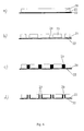
- the width of the furrows 24 corresponds to the width of the saw-blade used. This is shown at b.
- furrows 24 between the ICs 25 are filled with a light protecting material 23.
- the material 23 is dispensed into the furrows in a fluid or semi-fluid state, and subsequently hardens or solidifies.
- the furrows are now cut open once again, but this time using a saw with a smaller width. This provides new furrows 26 between the ICs 25, and at the same time leaves light protecting material 23 at the edges of each IC 25.
- the individual ICs can now be peeled off the sawing glue and are now ready for use in an apparatus.
- the front side is provided with components and solder bumps as described previously, (not shown in fig. 6 ) and has a lightprotecting layer, the back side is provided with the light protecting label 21, and the sides or edges are covered with the light protecting material 23. All processes have taken place at wafer level.
Landscapes
- Encapsulation Of And Coatings For Semiconductor Or Solid State Devices (AREA)
- Dicing (AREA)
Abstract
Description
- Integrated circuits (IC) are used in numerous electronic devices. One example of such a device is hearing aids wherein the integrated circuits are used for signal processing and amplification. The invention is especially relevant in connection with hearing aids, due to the required small size of these, but the invention is also relevant in any small size electronic device, in which speedy signal processing is required.
- Integrated circuits are produced on large silicon wafers and singulated before they are connected to a printed circuit board (PCB), usually by wire bonding from connection pads along the edge of the IC.
- In recent years a new process has been developed, in which a redistribution layer is applied to the surface of the IC, and an area array of solder bumps (ball grid array or BGA) is attached to the surface redistribution layer. These processes may be performed at the wafer level, and followed by singulation, and in some cases encapsulation for protection purposes. After singulation, the chip may be inverted, placed at a PCB, and by heating be attached through the BGA to the circuit board. Thereby the wire bonding can be omitted. Also it is known to stack various IC components using the BGA on one or both sides of the chips to gain connection between the stacked components.
- Usually IC's are mounted on printed circuit boards and gains contact with in and output signals and further electric components through the circuits on the circuit board. The circuit board is space consuming, and further the processes used to connect the IC to the circuits on the board requires multiple steps which all must be free of errors. Safe methods have been developed like the mentioned direct connection through a BGA, but long process times are still required. Further the voluminous printed circuit board is a major problem especially in hearing aids and similar electronic devices.
InUS patent 5563084 a method of making a three dimensionally integrated circuit is disclosed. First and second substrates are provided with devices in at least one layer in at least one surface each. An auxiliary substrate is connected to the one surface of the substrates, which is then reduced in thickness from its opposite surface. The auxiliary layer with the devices thereon is then separated into individual chips, which after having been found to be functioning are aligned and mounted in a side-by-side arrangement on the one surface of the first substrate. Electrical connections are formed between the devices of the mounted chips and the devices in the first substrate. The document does not disclose any way of protecting the individual dies in a wafer level process. -
US patent 6235141 discloses a mass production method for integrated optical subsystems. The invention concerns the alignement of singular dies with the dies in a wafer and subsequent bonding of the singular dies with the wafer. Following this the dies are diced to form a bonded pair of dies containing at least one optical element. The document does not disclose any way of protecting the individual dice in a wafer level process. -
US discloses a method for forming individual semiconductor devices by sandwiching a wafer with semiconductor elements on a first side thereon between two glass plates. The devices are diced by sawing.patent 6 177 295 - The object of the invention is to provide a method of producing a signal processing unit comprising an IC, which is faster and less prone to errors, and which is ready for use without the need of an underlying circuit board. In the following the signal processing unit is referred to as an amplifier, but any type of signal processing may take place in the unit.
- The objective is achieved with the method according to claim 1.
- Once an individual integrated circuit is singulated, and the protection of edges and possible unprotected side is ensured, the amplifier and signal processing unit is ready for use in a hearing aid or similar device. No mounting of the IC on a PCB is necessary, as the further electronic components required to produce the output signal from the integrated circuit are mounted on the surface or surfaces of each integrated circuit before singulation from the wafer. The formation of the furrows for the singulation may take place in any known manner eg. by sawing. Wires may be soldered directly to the solder connection pads for input and output signals and for current supply. The method according to claim 1 is both time saving and results in fewer errors, as the number of electric connections which must be established, is reduced. Further, handling of the individual integrated circuit after singulation is avoided, as singulation and coating for light and environmental protection is the last process the units are going through before mounting in the instrument in which they are to function.
- In a further embodiment of the method the following steps are performed:
- embedding a first side of the wafer in a polymer substance,
- providing a carrier layer to the polymer substance and hardening the polymer substance such that each amplifier and signal processing unit is retained embedded in the polymer substance and attached to the carrier,
- singulating the units from the opposite side of said first side of the wafer.
- If components are mounted on the first side of the wafer, they should be protected during singulation and this is done by embedding the components in a polymer substance, which will harden into an elastic layer, wherefrom the units at a later stage may be peeled off. If no components are present on the first side, the polymer substance acts primarily as an adhesive, which retains the wafer on the carrier layer. The polymer substance is also known as sawing glue.
- For handling purposes the carrier layer, preferably a rigid layer is provided at the polymer substance, such that the wafer in effect is glued to the carrier layer by the polymer substance. If components are only present at the first side of the wafer, the wafer may at this stage be thinned down by well-known back labbing methods. The advantage is that the rigid carrier layer facilitates handling and holding of the wafer during this operation. However if the chip has its final thickness no backlabbing will take place.
- After singulation of the units, they will still be attached to the carrier layer for subsequent operations, but they are easily peeled off.
- In an embodiment of the invention the singulation of the units is accomplished by means of V-shaped furrows through the thickness of the wafer provided along the edge of each integrated circuit. A conventional saw easily provides the V-shaped furrows, preferably a round saw. But other alternatives are known such as etching techniques ore laser cutting. The V-shape of the furrows makes subsequent coating of the side edges of the integrated circuit easy.
- In an embodiment the protection of the edges and possible unprotected side of the integrated circuits is accomplished by applying a protection layer to the integrated circuits. As the individual integrated circuits are still attached to the carrier layer, all the integrated circuits of a whole wafer may be treated simultaneously and a uniform protection layer may be accomplished. The protection layer protects the IC of the amplifier from light and other harmful environmental influences. The individual handling of the amplifiers during this delicate process is avoided.
- Preferably the protection layer is provided by metalization of the integrated circuits. In the case, where electric components are also attached to the back of the wafer, the metalization layer should only cover the edges of the integrated circuits. The use of metalization layers results in very dense and durable protection layers.
- In a further embodiment of the invention two or more carrier and/or information layers are applied to a first side of the wafer prior to singulation. Singulation is then carried out from the opposite side of the said first side of the wafer, and such that at least one information layer is severed along the edges of each integrated circuit, and such that the individual integrated circuits are retained on at least one un-severed carrier layer. The information layer, which is severed, remains with the individual integrated circuit. The un-severed carrier layer serves to keep the integrated circuits of the entire wafer together for further handling and treatment. After further treatment the individual integrated circuits may be peeled away from the carrier layer. The information layer which stays with the integrated circuit is preferably a printed label, where the carrier layer may comprise a sheet material or a sawing glue attached to the carrier plate.
- The space between the electrical components is filled with a suitable filler to produce a plane surface before the carrier and/or information layers are applied.
- Preferably the severed information layer is light protecting, and carries information concerning the identity of each integrated circuit.
- Preferably the carrier layer carrying the integrated circuits is an elastic layer, and said layer is stretched prior to coating the edges of the individual integrated circuits. By this stretching action the space between the individual integrated circuits is increased and more space is given for the coating of the edges of the integrated circuits.
- In an embodiment the protection layer for the edges is provided by filling the furrows with a fluid or semi-fluid substance, hardening the substance, providing a furrow between adjacent integrated circuits leaving the hardened substance attached to the edges of each integrated circuit. This embodiment provides an even and dense protection layer at all edges of the integrated circuit.
- The method according to the invention may be used for producing amplifier and signal processing units, wherein the solder connection pads and electrical components are provided on both sides of the wafer, and where through going apertures in the wafer are used to allow the I/O connections of the integrated circuit to gain contact with the solder connections on the opposite side of the wafer. The through going apertures must be provided at areas outside the area of the integrated circuit, but at the same time such that apertures are located within the perimeter and/or at the rim of each single integrated circuit.
-
-
FIG. 1 is a sectional view of an amplifier and signal processing units according to the prior art; -
FIG. 2 is a sectional view of an amplifier and signal processing units according to a first embodiment of the invention before singulation; -
FIG. 3 is a sectional view of an amplifier and signal processing units according to a first embodiment being prepared for singulation; -
FIG. 4 is a sectional view of an amplifier and signal processing units according to a second embodiment of the invention being prepared for singulation; -
FIG. 5 is a sectional view of the amplifier offig. 4 after singulation; -
FIG. 6 displays four steps of the protection and singulation according to a further embodiment of the invention. - The amplifier in
fig. 1 comprises anintegrated circuit 5 and a number of otherelectronic components 2 like resistors, capacitors or coils (only one component is shown). Theintegrated circuit 5 is mounted on asubstrate 18, like alumina ceramic, or pcb and bonded to thesubstrate 18. Thesubstrate 18 has vias (not shown) such that the connection points of theIC 5 gain contact with printed leads on the opposite side of thesubstrate 18. On thesubstrate 18 the otherelectronic components 2 are surface mounted and soldered to gain contact with the printed leads and through the vias to theIC 5. Also solder bumps 19 are provided for input, output and power supply for theIC 5. Achipcoat 20 is arranged on top and sides of theIC 5 for protection purposes. - In
fig. 2 a section through awafer 5 which has a number of integrated circuits on the topside is shown. The integrated circuits are arranged in a two-dimensional array as usual, and infig. 2 three of the integrated circuits of the wafer are shown. On top of the integrated circuits bonding pads (not shown) are provided, and through aredistribution layer 6 the bonding pads gain contact with soldering bumps 7. The integrated circuit under the redistribution layer must be protected from light and other harmful environmental influences. To do this a protection layer 9 is provided over theredistribution layer 6. The protection layer has apertures over the soldering bumps 7, and by filling the apertures with asuitable soldering material 8, connection to the soldering bumps 7 is achieved through the apertures. The protection layer must as a minimum requirement protect the IC from light. - Having established the protection layer and the
soldering material 8 over the soldering bumps 7,electronic components 2 are laid out on each integrated circuit of the wafer. The connection to the terminals of the components is established through heating whereby the soldering material melts. Further soldering points (not shown) for input, output and current supply are provided on each IC of the wafer. -
Fig. 3 shows the three integrated circuits offig. 2 after singulation and after aprotection layer 10 has been applied. Prior to the singulation, thecomponents 2 shown on the topside of the wafer are embedded in apolymer substance 11 such as a peelable solder mask. On top of the polymer substance 11 acarrier layer 12 is applied. The polymer substance is left to cure or solidify, which creates a firm bond between the wafer and thecarrier layer 12. The ICs may now be singulated, but will stay in their position on thecarrier layer 12. Preferably arigid carrier layer 12 is chosen. - The singulation may be performed in any known manner, and according to the invention a round saw having a blade with a V-shaped profile is used. Thereby V-shaped furrows, 13 are created between the individual ICs. The V-shaped furrows are preferably employed when the singulation takes place from the side opposite the side having the integrated circuit.
- The amplifiers shown in
fig. 3 may also have components mounted on the side opposite the side having the integrated circuit. In this case this side has a redistribution layer and a light protection layer corresponding to the layers provided on the top of the integrated circuit. Also connections through the wafer must be provided to allow connection between the redistribution layer on the opposite side and the integrated circuit. If components are mounted on both sides thelight protection layer 10 is only applied to the edges of the individual amplifiers. - After singulation the
entire carrier layer 12 having all ICs of the wafer is fed to a workstation for application of alight protection layer 10. This layer is preferably a metal layer, but other types of layers are possible. When the light protection layer is applied, the individual ICs may be peeled off thecarrier layer 12, leaving thepolymer substance 11 adhered at thecarrier layer 12. The light protection layer interconnects adjacent ICs at the bottom of the furrows, but as this layer is thin, it will brake when the ICs are peeled off the carrier layer. - In another embodiment of the invention shown in
fig. 4 and 5 the singulation of the wafers is accomplished after applicaton of aninformation layer 14 and acarrier layer 15. During the singulation theinformation layer 14 is severed, whereas the carrier layer stays intact. If singulation takes place from the side of the wafer having the integrated circuit, V shaped furrows cannot be used as in the previous example, (seefig. 3 ) but straight furrows must be used as shown infig. 5 . This is because the integrated circuits are produced on the wafer with a minimum of space there between. However if the singulation takes place from the side opposite the side of the integrated circuit, a V shaped furrow may be used for the singulation. - The singulated ICs are treated at the
edges 18 by aprotection layer 17 as shown infig. 5 . Infig. 4 and 5 no electrical components are shown at the side whereto the information and carrier layers 14,15 are applied, but components may be present, and in this case a filler is introduced between the component. The filler is used to provide a uniform and even surface, whereto the information and carrier layers 14,15 may be applied. The filler is preferably a polymer which may be applied in fluid or semifluid state, and which is left to cure, before application of the information and carrier layers 14, 15. Theinformation layer 14 should be light and environmentally protecting if thelayer 14 is applied directly to the surface of the wafer as shown infig. 4 and 5 . Thereby the necessary protection of the wafer is provided. Theinformation layer 14 is preferably a pre-printed label, which carries information identifying each amplifier. - The
carrier layer 15 could be any coherent substance, which will keep the singulated ICs together for subsequent treatment. A rigid plate could be used and in this case an adhesive must be introduced between thecarrier 15 layer and theinformation layer 14. In one embodiment thecarrier layer 15 is a flexible sheet whereto the ICs are adhered. Such a flexible sheet may be stretched to some extent, and this will provide more space 16 between the individual ICs for application of thelight protection layer 17 to theedges 18 of the ICs. - The
carrier layer 12 of the embodiment according tofig. 3 and thecarrier layer 15 according tofig. 4 may look different, but in fact they serve the same overall purpose, namely to retain all of the amplifiers of the wafer attached and together during the singulation and during subsequent processing such as applying light protection coating to the edges of the ICs. - In the embodiment according to
fig. 6 four steps in the process of protection and singulation a, b, c and d are shown. At a, thewafer 20 is supplied with alabel 21 and fastened at the label side in a sawingglue 22. Following this theindividual ICs 25 are singulated using standard sawing techniques but such that thelabel 21 is also cut. - This creates furrows 24 between all
ICs 25 and they are now maintained in position by their adhesion to the sawingglue 22. The width of thefurrows 24 corresponds to the width of the saw-blade used. This is shown at b. At c it is shown how thefurrows 24 between theICs 25 are filled with a light protecting material 23. The material 23 is dispensed into the furrows in a fluid or semi-fluid state, and subsequently hardens or solidifies. In the last processing step shown at d the furrows are now cut open once again, but this time using a saw with a smaller width. This providesnew furrows 26 between theICs 25, and at the same time leaves light protecting material 23 at the edges of eachIC 25. The individual ICs can now be peeled off the sawing glue and are now ready for use in an apparatus. The front side is provided with components and solder bumps as described previously, (not shown infig. 6 ) and has a lightprotecting layer, the back side is provided with thelight protecting label 21, and the sides or edges are covered with the light protecting material 23. All processes have taken place at wafer level.
Claims (12)
- Method for producing an amplifier and signal processing unit ready for use in a hearing aid with an integrated circuit and all further components required to produce the amplified output signal comprising the steps of :- producing arrays of individual integrated circuits on a side of a wafer (5), where each circuit has a number of I/O connection points;- providing a number of solder connection pads (7) at each integrated circuit for redistribution of the I/O connection points of the integrated circuit;- coating the side of the wafer having the solder connection pads (7) with a coating of protection material (9) and ensuring through-going apertures (8) in the coating to provide electrical contact with the solder connection pads (7);- applying electrical components (2) onto the coating and gaining electrical contact with the solder connection pads (7) through the apertures (8) of the protection material (9) prior to a step of singulating the individual integrated circuits in order to form the amplifier and signal processing units;- fastening the wafer (5) to a carrier layer,- singulating the individual amplifier and signal processing units by providing furrows along the edges of each integrated circuit through the thickness of the wafer and- ensuring protection of the edges of the integrated circuit while the individual integrated circuits remain fastened to the carrier layer.
- Method according to claim 1, wherein the following steps are performed:- embedding a first side of the wafer (5) in a polymer substance (11);- providing the carrier layer (12) to the polymer substance (11) and hardening the polymer substance (11) such that each amplifier and signal processing units is retained embedded in the polymer substance (11) and attached to the carrier layer (12);- singulating the amplifier and signal processing units from the opposite side of said first side of the wafer.
- Method according to claim 1 or 2, wherein the singulation of the amplifiers and signal processing units is accomplished by means of v-shaped furrows (13) through the thickness of the wafer (5) provided along the edge of each integrated circuit.
- Method according to claim 2 or 3, wherein the protection of the edges and possible unprotected side of the integrated circuits is accomplished by applying a protection layer (10) to the integrated circuits.
- Method according to claim 4, wherein the protection layer (10) is provided by metalization of the integrated circuits.
- Method according to claim 1, wherein two or more carrier and/or information layers (14;15) are applied to a first side of the wafer (5) prior to singulation, and wherein singulation is carried out from the opposite side of said first side by providing furrows through the thickness of the wafer, and such that at least one information layer (14) is severed along the edges of each integrated circuit, and such that the individual integrated circuits are retained on at least one un-severed carrierlayer (15).
- Method according to claim 6, wherein electrical components are present at the first side of the integrated circuits, and wherein the space between the components is filled with a filler material to produce a plane surface prior to application of the carrier and/or information layers (14;15) to the first side of the wafer (5).
- Method according to claim 6 or 7, wherein the severed information layer (14) is light protecting, and carries information concerning the identity of each integrated circuit.
- Method according to claim 8, wherein the carrier layer (15) carrying the amplifier and signal processing units is an elastic layer, and that said layer (15) is stretched prior to coating the edges (18) of the individual integrated circuits.
- Method according to claims 1-4 or 6, wherein the protection layer is provided by:filling the furrows with a fluid or semi-fluid substance, hardening the substance, providing a furrow between adjacent amplifier and signal processing units leaving the hardened substance attached to the edges of each integrated circuit.
- Method according to claim 9, wherein the amplifier and signal processing units are peeled off the carrier layer (15) after singulation and coating.
- Method according to any of claims 1-11, wherein the solder connection pads (8) and electrical components (2) are provided on both sides of the wafer (5), and that through going apertures are used to allow the I/O connections of the integrated circuit to gain contact with the solder connections on the opposite side of the wafer (5).
Applications Claiming Priority (3)
| Application Number | Priority Date | Filing Date | Title |
|---|---|---|---|
| DK200100942 | 2001-06-16 | ||
| DKPA200100942 | 2001-06-16 | ||
| PCT/DK2002/000402 WO2002103784A1 (en) | 2001-06-16 | 2002-06-14 | Method for producing miniature amplifier and signal processing unit |
Publications (2)
| Publication Number | Publication Date |
|---|---|
| EP1402572A1 EP1402572A1 (en) | 2004-03-31 |
| EP1402572B1 true EP1402572B1 (en) | 2013-12-18 |
Family
ID=8160567
Family Applications (1)
| Application Number | Title | Priority Date | Filing Date |
|---|---|---|---|
| EP02748619.0A Expired - Lifetime EP1402572B1 (en) | 2001-06-16 | 2002-06-14 | Method for producing miniature amplifier and signal processing unit |
Country Status (5)
| Country | Link |
|---|---|
| US (1) | US7011985B2 (en) |
| EP (1) | EP1402572B1 (en) |
| JP (1) | JP4276535B2 (en) |
| DK (1) | DK1402572T3 (en) |
| WO (1) | WO2002103784A1 (en) |
Families Citing this family (5)
| Publication number | Priority date | Publication date | Assignee | Title |
|---|---|---|---|---|
| WO2002103784A1 (en) * | 2001-06-16 | 2002-12-27 | Oticon A/S | Method for producing miniature amplifier and signal processing unit |
| DE10253163B4 (en) * | 2002-11-14 | 2015-07-23 | Epcos Ag | Hermetic encapsulation device and wafer scale manufacturing method |
| DE102007030284B4 (en) | 2007-06-29 | 2009-12-31 | Schott Ag | Process for packaging semiconductor devices and intermediate product produced by the process |
| DE102007035902A1 (en) * | 2007-07-31 | 2009-02-05 | Siemens Ag | Method for producing an electronic component and electronic component |
| US9064881B2 (en) * | 2010-11-11 | 2015-06-23 | Taiwan Semiconductor Manufacturing Company, Ltd. | Protecting flip-chip package using pre-applied fillet |
Family Cites Families (6)
| Publication number | Priority date | Publication date | Assignee | Title |
|---|---|---|---|---|
| US6728113B1 (en) * | 1993-06-24 | 2004-04-27 | Polychip, Inc. | Method and apparatus for non-conductively interconnecting integrated circuits |
| US6245595B1 (en) * | 1999-07-22 | 2001-06-12 | National Semiconductor Corporation | Techniques for wafer level molding of underfill encapsulant |
| US6338980B1 (en) * | 1999-08-13 | 2002-01-15 | Citizen Watch Co., Ltd. | Method for manufacturing chip-scale package and manufacturing IC chip |
| JP2001127206A (en) * | 1999-08-13 | 2001-05-11 | Citizen Watch Co Ltd | Method of manufacturing chip scale package and method of manufacturing IC chip |
| JP3609692B2 (en) * | 2000-05-24 | 2005-01-12 | 松下電器産業株式会社 | High frequency signal amplifying device and method for manufacturing the same |
| WO2002103784A1 (en) * | 2001-06-16 | 2002-12-27 | Oticon A/S | Method for producing miniature amplifier and signal processing unit |
-
2002
- 2002-06-14 WO PCT/DK2002/000402 patent/WO2002103784A1/en not_active Ceased
- 2002-06-14 EP EP02748619.0A patent/EP1402572B1/en not_active Expired - Lifetime
- 2002-06-14 US US10/484,246 patent/US7011985B2/en not_active Expired - Fee Related
- 2002-06-14 JP JP2003505998A patent/JP4276535B2/en not_active Expired - Lifetime
- 2002-06-14 DK DK02748619.0T patent/DK1402572T3/en active
Also Published As
| Publication number | Publication date |
|---|---|
| DK1402572T3 (en) | 2014-03-17 |
| EP1402572A1 (en) | 2004-03-31 |
| US7011985B2 (en) | 2006-03-14 |
| US20040235218A1 (en) | 2004-11-25 |
| JP2004531071A (en) | 2004-10-07 |
| WO2002103784A1 (en) | 2002-12-27 |
| JP4276535B2 (en) | 2009-06-10 |
Similar Documents
| Publication | Publication Date | Title |
|---|---|---|
| US7863757B2 (en) | Methods and systems for packaging integrated circuits | |
| US6399415B1 (en) | Electrical isolation in panels of leadless IC packages | |
| US8533941B2 (en) | Method of bonding two structures together with an adhesive line of controlled thickness | |
| US8048781B2 (en) | Methods and systems for packaging integrated circuits | |
| JP3456462B2 (en) | Semiconductor device and manufacturing method thereof | |
| US8173488B2 (en) | Electronic device and method of manufacturing same | |
| US20030082890A1 (en) | Fan out of interconnect elements attached to semiconductor wafer | |
| US8389334B2 (en) | Foil-based method for packaging intergrated circuits | |
| CN101553923A (en) | Edge connected wafer level stacking | |
| IE56411B1 (en) | Integrated circuit chip carrier | |
| US6500764B1 (en) | Method for thinning a semiconductor substrate | |
| US7011985B2 (en) | Method for producing miniature amplifier and signal processing unit | |
| JP2008130704A (en) | Manufacturing method of semiconductor device | |
| US20210309512A1 (en) | Method for manufacturing a mems sensor | |
| US20080029865A1 (en) | Electronic Device and Method For Producing the Same | |
| US8030138B1 (en) | Methods and systems of packaging integrated circuits | |
| KR100927778B1 (en) | Semiconductor Package Manufacturing Method | |
| US6867065B2 (en) | Method of making a microelectronic assembly | |
| US20060099735A1 (en) | Method for wafer level stack die placement | |
| JP2001085363A (en) | Method for manufacturing semiconductor device | |
| US6551855B1 (en) | Substrate strip and manufacturing method thereof | |
| US7485493B2 (en) | Singulating surface-mountable semiconductor devices and fitting external contacts to said devices | |
| US20260040958A1 (en) | Isolation for chip on lead device and manufacturing method | |
| JP2004327724A (en) | Semiconductor device and manufacturing method thereof | |
| JP4218337B2 (en) | Manufacturing method of semiconductor device |
Legal Events
| Date | Code | Title | Description |
|---|---|---|---|
| PUAI | Public reference made under article 153(3) epc to a published international application that has entered the european phase |
Free format text: ORIGINAL CODE: 0009012 |
|
| 17P | Request for examination filed |
Effective date: 20040116 |
|
| AK | Designated contracting states |
Kind code of ref document: A1 Designated state(s): AT BE CH CY DE DK ES FI FR GB GR IE IT LI LU MC NL PT SE TR |
|
| RAP1 | Party data changed (applicant data changed or rights of an application transferred) |
Owner name: OTICON A/S |
|
| 17Q | First examination report despatched |
Effective date: 20061130 |
|
| GRAP | Despatch of communication of intention to grant a patent |
Free format text: ORIGINAL CODE: EPIDOSNIGR1 |
|
| RIC1 | Information provided on ipc code assigned before grant |
Ipc: H01L 21/78 20060101AFI20130614BHEP Ipc: H01L 21/683 20060101ALI20130614BHEP Ipc: H01L 23/31 20060101ALI20130614BHEP Ipc: H01L 23/00 20060101ALI20130614BHEP Ipc: H01L 21/56 20060101ALI20130614BHEP Ipc: H01L 21/68 20060101ALI20130614BHEP |
|
| INTG | Intention to grant announced |
Effective date: 20130717 |
|
| GRAS | Grant fee paid |
Free format text: ORIGINAL CODE: EPIDOSNIGR3 |
|
| GRAA | (expected) grant |
Free format text: ORIGINAL CODE: 0009210 |
|
| AK | Designated contracting states |
Kind code of ref document: B1 Designated state(s): AT BE CH CY DE DK ES FI FR GB GR IE IT LI LU MC NL PT SE TR |
|
| REG | Reference to a national code |
Ref country code: GB Ref legal event code: FG4D |
|
| REG | Reference to a national code |
Ref country code: CH Ref legal event code: EP |
|
| REG | Reference to a national code |
Ref country code: AT Ref legal event code: REF Ref document number: 645942 Country of ref document: AT Kind code of ref document: T Effective date: 20140115 |
|
| REG | Reference to a national code |
Ref country code: IE Ref legal event code: FG4D |
|
| REG | Reference to a national code |
Ref country code: DE Ref legal event code: R096 Ref document number: 60245859 Country of ref document: DE Effective date: 20140213 |
|
| REG | Reference to a national code |
Ref country code: DK Ref legal event code: T3 Effective date: 20140311 |
|
| REG | Reference to a national code |
Ref country code: NL Ref legal event code: VDEP Effective date: 20131218 |
|
| PG25 | Lapsed in a contracting state [announced via postgrant information from national office to epo] |
Ref country code: SE Free format text: LAPSE BECAUSE OF FAILURE TO SUBMIT A TRANSLATION OF THE DESCRIPTION OR TO PAY THE FEE WITHIN THE PRESCRIBED TIME-LIMIT Effective date: 20131218 Ref country code: FI Free format text: LAPSE BECAUSE OF FAILURE TO SUBMIT A TRANSLATION OF THE DESCRIPTION OR TO PAY THE FEE WITHIN THE PRESCRIBED TIME-LIMIT Effective date: 20131218 |
|
| REG | Reference to a national code |
Ref country code: AT Ref legal event code: MK05 Ref document number: 645942 Country of ref document: AT Kind code of ref document: T Effective date: 20131218 |
|
| PG25 | Lapsed in a contracting state [announced via postgrant information from national office to epo] |
Ref country code: BE Free format text: LAPSE BECAUSE OF FAILURE TO SUBMIT A TRANSLATION OF THE DESCRIPTION OR TO PAY THE FEE WITHIN THE PRESCRIBED TIME-LIMIT Effective date: 20131218 |
|
| PG25 | Lapsed in a contracting state [announced via postgrant information from national office to epo] |
Ref country code: ES Free format text: LAPSE BECAUSE OF FAILURE TO SUBMIT A TRANSLATION OF THE DESCRIPTION OR TO PAY THE FEE WITHIN THE PRESCRIBED TIME-LIMIT Effective date: 20131218 Ref country code: AT Free format text: LAPSE BECAUSE OF FAILURE TO SUBMIT A TRANSLATION OF THE DESCRIPTION OR TO PAY THE FEE WITHIN THE PRESCRIBED TIME-LIMIT Effective date: 20131218 Ref country code: CY Free format text: LAPSE BECAUSE OF FAILURE TO SUBMIT A TRANSLATION OF THE DESCRIPTION OR TO PAY THE FEE WITHIN THE PRESCRIBED TIME-LIMIT Effective date: 20131218 Ref country code: NL Free format text: LAPSE BECAUSE OF FAILURE TO SUBMIT A TRANSLATION OF THE DESCRIPTION OR TO PAY THE FEE WITHIN THE PRESCRIBED TIME-LIMIT Effective date: 20131218 Ref country code: PT Free format text: LAPSE BECAUSE OF FAILURE TO SUBMIT A TRANSLATION OF THE DESCRIPTION OR TO PAY THE FEE WITHIN THE PRESCRIBED TIME-LIMIT Effective date: 20140418 |
|
| REG | Reference to a national code |
Ref country code: DE Ref legal event code: R097 Ref document number: 60245859 Country of ref document: DE |
|
| PLBE | No opposition filed within time limit |
Free format text: ORIGINAL CODE: 0009261 |
|
| STAA | Information on the status of an ep patent application or granted ep patent |
Free format text: STATUS: NO OPPOSITION FILED WITHIN TIME LIMIT |
|
| 26N | No opposition filed |
Effective date: 20140919 |
|
| REG | Reference to a national code |
Ref country code: DE Ref legal event code: R097 Ref document number: 60245859 Country of ref document: DE Effective date: 20140919 |
|
| PG25 | Lapsed in a contracting state [announced via postgrant information from national office to epo] |
Ref country code: MC Free format text: LAPSE BECAUSE OF FAILURE TO SUBMIT A TRANSLATION OF THE DESCRIPTION OR TO PAY THE FEE WITHIN THE PRESCRIBED TIME-LIMIT Effective date: 20131218 Ref country code: LU Free format text: LAPSE BECAUSE OF FAILURE TO SUBMIT A TRANSLATION OF THE DESCRIPTION OR TO PAY THE FEE WITHIN THE PRESCRIBED TIME-LIMIT Effective date: 20140614 |
|
| REG | Reference to a national code |
Ref country code: IE Ref legal event code: MM4A |
|
| PG25 | Lapsed in a contracting state [announced via postgrant information from national office to epo] |
Ref country code: IE Free format text: LAPSE BECAUSE OF NON-PAYMENT OF DUE FEES Effective date: 20140614 |
|
| REG | Reference to a national code |
Ref country code: FR Ref legal event code: PLFP Year of fee payment: 14 |
|
| PGFP | Annual fee paid to national office [announced via postgrant information from national office to epo] |
Ref country code: CH Payment date: 20150612 Year of fee payment: 14 Ref country code: DK Payment date: 20150602 Year of fee payment: 14 Ref country code: GB Payment date: 20150602 Year of fee payment: 14 Ref country code: DE Payment date: 20150624 Year of fee payment: 14 |
|
| PGFP | Annual fee paid to national office [announced via postgrant information from national office to epo] |
Ref country code: FR Payment date: 20150630 Year of fee payment: 14 |
|
| PG25 | Lapsed in a contracting state [announced via postgrant information from national office to epo] |
Ref country code: GR Free format text: LAPSE BECAUSE OF FAILURE TO SUBMIT A TRANSLATION OF THE DESCRIPTION OR TO PAY THE FEE WITHIN THE PRESCRIBED TIME-LIMIT Effective date: 20140319 Ref country code: IT Free format text: LAPSE BECAUSE OF FAILURE TO SUBMIT A TRANSLATION OF THE DESCRIPTION OR TO PAY THE FEE WITHIN THE PRESCRIBED TIME-LIMIT Effective date: 20131218 |
|
| PG25 | Lapsed in a contracting state [announced via postgrant information from national office to epo] |
Ref country code: TR Free format text: LAPSE BECAUSE OF FAILURE TO SUBMIT A TRANSLATION OF THE DESCRIPTION OR TO PAY THE FEE WITHIN THE PRESCRIBED TIME-LIMIT Effective date: 20131218 |
|
| REG | Reference to a national code |
Ref country code: DE Ref legal event code: R119 Ref document number: 60245859 Country of ref document: DE |
|
| REG | Reference to a national code |
Ref country code: DK Ref legal event code: EBP Effective date: 20160630 |
|
| REG | Reference to a national code |
Ref country code: CH Ref legal event code: PL |
|
| GBPC | Gb: european patent ceased through non-payment of renewal fee |
Effective date: 20160614 |
|
| REG | Reference to a national code |
Ref country code: FR Ref legal event code: ST Effective date: 20170228 |
|
| PG25 | Lapsed in a contracting state [announced via postgrant information from national office to epo] |
Ref country code: LI Free format text: LAPSE BECAUSE OF NON-PAYMENT OF DUE FEES Effective date: 20160630 Ref country code: CH Free format text: LAPSE BECAUSE OF NON-PAYMENT OF DUE FEES Effective date: 20160630 Ref country code: FR Free format text: LAPSE BECAUSE OF NON-PAYMENT OF DUE FEES Effective date: 20160630 Ref country code: DE Free format text: LAPSE BECAUSE OF NON-PAYMENT OF DUE FEES Effective date: 20170103 |
|
| PG25 | Lapsed in a contracting state [announced via postgrant information from national office to epo] |
Ref country code: GB Free format text: LAPSE BECAUSE OF NON-PAYMENT OF DUE FEES Effective date: 20160614 |
|
| PG25 | Lapsed in a contracting state [announced via postgrant information from national office to epo] |
Ref country code: DK Free format text: LAPSE BECAUSE OF NON-PAYMENT OF DUE FEES Effective date: 20160630 |