EP1401091A1 - Cold-cathode driver and liquid crystal display - Google Patents
Cold-cathode driver and liquid crystal display Download PDFInfo
- Publication number
- EP1401091A1 EP1401091A1 EP02743726A EP02743726A EP1401091A1 EP 1401091 A1 EP1401091 A1 EP 1401091A1 EP 02743726 A EP02743726 A EP 02743726A EP 02743726 A EP02743726 A EP 02743726A EP 1401091 A1 EP1401091 A1 EP 1401091A1
- Authority
- EP
- European Patent Office
- Prior art keywords
- pulse
- pulse width
- frequency
- cold cathode
- distribution
- Prior art date
- Legal status (The legal status is an assumption and is not a legal conclusion. Google has not performed a legal analysis and makes no representation as to the accuracy of the status listed.)
- Withdrawn
Links
Images




















Classifications
-
- H—ELECTRICITY
- H05—ELECTRIC TECHNIQUES NOT OTHERWISE PROVIDED FOR
- H05B—ELECTRIC HEATING; ELECTRIC LIGHT SOURCES NOT OTHERWISE PROVIDED FOR; CIRCUIT ARRANGEMENTS FOR ELECTRIC LIGHT SOURCES, IN GENERAL
- H05B41/00—Circuit arrangements or apparatus for igniting or operating discharge lamps
- H05B41/14—Circuit arrangements
- H05B41/36—Controlling
- H05B41/38—Controlling the intensity of light
- H05B41/39—Controlling the intensity of light continuously
- H05B41/392—Controlling the intensity of light continuously using semiconductor devices, e.g. thyristor
- H05B41/3921—Controlling the intensity of light continuously using semiconductor devices, e.g. thyristor with possibility of light intensity variations
- H05B41/3925—Controlling the intensity of light continuously using semiconductor devices, e.g. thyristor with possibility of light intensity variations by frequency variation
-
- H—ELECTRICITY
- H05—ELECTRIC TECHNIQUES NOT OTHERWISE PROVIDED FOR
- H05B—ELECTRIC HEATING; ELECTRIC LIGHT SOURCES NOT OTHERWISE PROVIDED FOR; CIRCUIT ARRANGEMENTS FOR ELECTRIC LIGHT SOURCES, IN GENERAL
- H05B41/00—Circuit arrangements or apparatus for igniting or operating discharge lamps
- H05B41/14—Circuit arrangements
- H05B41/26—Circuit arrangements in which the lamp is fed by power derived from DC by means of a converter, e.g. by high-voltage DC
- H05B41/28—Circuit arrangements in which the lamp is fed by power derived from DC by means of a converter, e.g. by high-voltage DC using static converters
- H05B41/282—Circuit arrangements in which the lamp is fed by power derived from DC by means of a converter, e.g. by high-voltage DC using static converters with semiconductor devices
- H05B41/2821—Circuit arrangements in which the lamp is fed by power derived from DC by means of a converter, e.g. by high-voltage DC using static converters with semiconductor devices by means of a single-switch converter or a parallel push-pull converter in the final stage
- H05B41/2822—Circuit arrangements in which the lamp is fed by power derived from DC by means of a converter, e.g. by high-voltage DC using static converters with semiconductor devices by means of a single-switch converter or a parallel push-pull converter in the final stage using specially adapted components in the load circuit, e.g. feed-back transformers, piezoelectric transformers; using specially adapted load circuit configurations
-
- H—ELECTRICITY
- H05—ELECTRIC TECHNIQUES NOT OTHERWISE PROVIDED FOR
- H05B—ELECTRIC HEATING; ELECTRIC LIGHT SOURCES NOT OTHERWISE PROVIDED FOR; CIRCUIT ARRANGEMENTS FOR ELECTRIC LIGHT SOURCES, IN GENERAL
- H05B41/00—Circuit arrangements or apparatus for igniting or operating discharge lamps
- H05B41/14—Circuit arrangements
- H05B41/26—Circuit arrangements in which the lamp is fed by power derived from DC by means of a converter, e.g. by high-voltage DC
- H05B41/28—Circuit arrangements in which the lamp is fed by power derived from DC by means of a converter, e.g. by high-voltage DC using static converters
- H05B41/282—Circuit arrangements in which the lamp is fed by power derived from DC by means of a converter, e.g. by high-voltage DC using static converters with semiconductor devices
- H05B41/2821—Circuit arrangements in which the lamp is fed by power derived from DC by means of a converter, e.g. by high-voltage DC using static converters with semiconductor devices by means of a single-switch converter or a parallel push-pull converter in the final stage
- H05B41/2824—Circuit arrangements in which the lamp is fed by power derived from DC by means of a converter, e.g. by high-voltage DC using static converters with semiconductor devices by means of a single-switch converter or a parallel push-pull converter in the final stage using control circuits for the switching element
-
- H—ELECTRICITY
- H05—ELECTRIC TECHNIQUES NOT OTHERWISE PROVIDED FOR
- H05B—ELECTRIC HEATING; ELECTRIC LIGHT SOURCES NOT OTHERWISE PROVIDED FOR; CIRCUIT ARRANGEMENTS FOR ELECTRIC LIGHT SOURCES, IN GENERAL
- H05B41/00—Circuit arrangements or apparatus for igniting or operating discharge lamps
- H05B41/14—Circuit arrangements
- H05B41/36—Controlling
- H05B41/38—Controlling the intensity of light
- H05B41/39—Controlling the intensity of light continuously
- H05B41/392—Controlling the intensity of light continuously using semiconductor devices, e.g. thyristor
- H05B41/3921—Controlling the intensity of light continuously using semiconductor devices, e.g. thyristor with possibility of light intensity variations
- H05B41/3927—Controlling the intensity of light continuously using semiconductor devices, e.g. thyristor with possibility of light intensity variations by pulse width modulation
-
- Y—GENERAL TAGGING OF NEW TECHNOLOGICAL DEVELOPMENTS; GENERAL TAGGING OF CROSS-SECTIONAL TECHNOLOGIES SPANNING OVER SEVERAL SECTIONS OF THE IPC; TECHNICAL SUBJECTS COVERED BY FORMER USPC CROSS-REFERENCE ART COLLECTIONS [XRACs] AND DIGESTS
- Y02—TECHNOLOGIES OR APPLICATIONS FOR MITIGATION OR ADAPTATION AGAINST CLIMATE CHANGE
- Y02B—CLIMATE CHANGE MITIGATION TECHNOLOGIES RELATED TO BUILDINGS, e.g. HOUSING, HOUSE APPLIANCES OR RELATED END-USER APPLICATIONS
- Y02B20/00—Energy efficient lighting technologies, e.g. halogen lamps or gas discharge lamps
Definitions
- the present invention relates to a cold cathode tube driving device which utilizes a piezoelectric transformer as a booster transformer for driving a cold cathode tube, for example, a backlight of a liquid crystal panel, and a liquid crystal display device on which the cold cathode tube driving device is mounted.
- a piezoelectric transformer that can be reduced in size and thickness and can bring high efficiency has been used, instead of an electromagnetic transformer, as a booster transformer for driving a cold cathode tube that is a backlight of a liquid crystal panel.
- the piezoelectric transformer is generally a voltage converting element, which utilizes the piezoelectric effect of a piezoelectric element for generating mechanical oscillations and taking out from its secondary electrode side a voltage amplified depending on a voltage step-up ratio determined by the shape of the piezoelectric transformer.
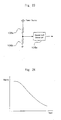
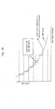
- Fig. 40 shows a general characteristic of a piezoelectric transformer.
- an output voltage at its secondary side varies in accordance with a frequency of an AC voltage inputted to its primary side since the piezoelectric transformer has a resonance characteristic.
- the next form is popular as a method for controlling the brightness of the backlight at a constant level. Specifically, this method is such that the frequency of the AC voltage for driving the piezoelectric transformer is controlled to obtain an amplitude of a desired level at the secondary side, to thereby apply a stable voltage to the cold cathode tube.
- a linear inclined portion in the frequency area higher than the resonance frequency is utilized for the control.
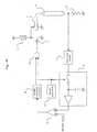
- Fig. 41 shows a general configuration of a backlight drivingmeans.
- numeral 1 designates a piezoelectric transformer, 2 a coil, 3 a switching transistor (FET (Field Effect Transistor)), 4 a cold cathode tube, 5 a current detector for detecting electric current flowing through the cold cathode tube 4 and 6 a driving pulse generating circuit that compares the detected voltage by the current detector 5 with a reference voltage for producing a driving pulse of a frequency according to its difference.
- FET Field Effect Transistor
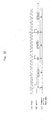
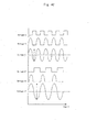
- Fig. 42 shows waveforms at each means of the circuit shown in Fig. 41.
- a voltage A is an output voltage waveform (driving pulse) of the driving pulse generating circuit 6
- a voltage B is an input voltage waveform of the piezoelectric transformer 1
- a voltage C is an output voltage waveform of the piezoelectric transformer 1.
- the voltage C is given to the cold cathode tube 4 so that electric current (tube current) flows through the cold cathode tube 4.
- the current flowing through the cold cathode tube 4 is detected by the current detector 5.
- the input voltage of the piezoelectric transformer 1 is desirably a sinusoidal voltage, the following explanation is made with a half-wave sinusoidal voltage.
- the coil 2 and the piezoelectric transformer 1 constitute a resonance circuit. Its resonance frequency is determined by the inductance value of the coil 2 and the input capacity value of the piezoelectric transformer 1.
- Applying energy to the resonance circuit via the FET 3 brings a half-wave sinusoidal voltage with the above-mentioned resonance frequency (voltage B). Only the resonance frequency component possessed by the piezoelectric transformer 1 itself is drawn out from the output of the piezoelectric transformer 1 to.which the voltage B is inputted, with the result that the sinusoidal voltage that is the voltage C shown in Fig. 42 is outputted.
- This sinusoidal voltage C has the amplitude varying in accordance with the frequency of the voltage B due to the characteristic shown in Fig. 40.
- the driving pulse generating circuit 6 compares the voltage obtained from the current detector 5 with the reference voltage for controlling the frequency of the output voltage from the driving pulse generating circuit 6 such that the tube current is made to be a desired value.
- Voltages Al to Cl in Fig. 42 respectively show waveforms of each means when the frequency of the driving pulse is lowered. The lower the frequency becomes, the greater the amplitude of the sinusoidal voltage becomes.
- a method for controlling the tube current by varying the frequency of the driving pulse is generally used for controlling the brightness of the cold cathode tube 4 in the driving circuit of the piezoelectric transformer 1.
- a circuit for realizing the above-mentioned technique has generally been formed of an analog circuit. Accordingly, there is a problem that the number of components is increased and the space for the components is large. Particularly, it has been desired that the space for the driving circuit is saved since miniaturization of equipment is important in a portable imaging equipment such as a VTR integrated with a camera or a digital camera.
- the technique in the document 1 is a system in which a frequency of the driving pulse is distributed. This system enables a dimming resolution by a frequency control with approximately 10 MHz clocks.
- the frequency resolution of only about 1 KHz can be obtained in the vicinity of 100 KHz, so that it is difficult to realize not only dimming performance but also stable lighting.
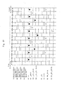
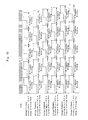
- a configuration is made such that a frequency dividing ratio is distributed in a predetermined driving cycle for obtaining a resolution with an average frequency as shown in Fig. 43.
- a frequency dividing ratio is distributed in 100 cycles, for example, a hundred-fold frequency resolution can be obtained.
- This method enables to incorporate a cold cathode tube driving device in a digital LSI, thereby being capable of reducing a space and cost.
- the driving method disclosed in the document 1 is a system for performing the dimming control by controlling. the tube current.
- this method for performing the dimming control by controlling the tube current has the following problems:
- a burst dimming in which the driving is intermittently turned on and off at a frequency (for example, about 100 Hz) that does not cause a brightness flicker.
- the dimming level is changed by changing a duty ratio of turning-on and turning-off.
- This technique has widely been used for not only a backlight driving circuit utilizing a piezoelectric transformer but also a backlight driving circuit utilizing a conventional electromagnetic transformer.
- the former method can be adopted to the conventional circuit.
- a starting control upon turning on a power source and a normal control upon lighting are repeatedly executed.
- a shield circuit for turning on and turning off the power source is required in a power source line. An electric loss occurs due to this shield circuit, thus not preferable in a portable equipment in particular.
- the latter method requires a means for turning off the detection of the tube current upon turning off the driving and holding the driving frequency at a predetermined value in addition to the conventional circuit. In this case, there is no electric loss in the power source line, thus excellent in the use of a portable equipment in particular.
- a technique for realizing this method in an analog system is disclosed, for example, in Japanese Unexamined Patent Publication No. 11-298060 (1999) (document 2).
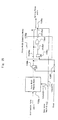
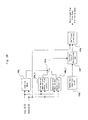
- Fig. 44 is a view simplifying the technique disclosed in the document 2. It is featured in that a voltage at the current detector 5 is held by a sample holding means 8 upon turning off the driving, thereby holding the oscillation frequency of a voltage control oscillation circuit 12 at a constant level and promptly starting the lighting upon restarting the driving.
- the burst dimming driving system can be realized by adding a simple circuit in the analog driving system.
- the burst dimming is realized in the digital system by a frequency distribution system, there arises the following subjects:
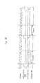
- the first one is a method for performing with the burst driving upon the starting similar to the case upon the lighting as shown in Fig. 46. This method does not require extra circuits since the burst control is adopted upon starting and lighting. Further, the brightness level is shifted to the aimed brightness level without sense of a incongruity, thereby being capable of obtaining a satisfactory lighting quality.
- the lighting performance of the cold cathode tube is deteriorated in this method, especially in case where the aimed brightness level is low.
- a cold cathode tube generally has reduced lighting performance at a low temperature or under a dark ambient illuminance. This problem has been known to be improved by rising the starting voltage or lengthening time for applying the starting voltage.
- the starting with the burst driving requires an extra time for applying the starting voltage, thereby taking time to light.
- a protection function is provided to terminate the starting unless lighting is executed even after a predetermined period. There may be the case where lighting is not executed due to the influence of this protection function.
- the second method is that, as shown in Fig. 47, continuous driving is performed upon the starting in view of the lighting performance of the cold cathode tube, and then, the driving is promptly shifted to the burst driving after the lighting.
- This method requires a lighting detecting means and a control switching means since the control is different between upon the starting and upon the lighting. If an ideal lighting detecting means can be obtained, it enables the lighting with the aimed brightness level without deteriorating the lighting performance of the cold cathode tube.
- the conventional lighting detecting means is slow in detecting the lighting, resulting in that the brightness is greatly changed by the time of reaching the aimed brightness level as shown in Fig. 47, that causes a problem concerning the lighting quality.
- the present invention is accomplished in view of the above-mentioned problems, and an object thereof is to firstly propose a driving system realizing a burst dimming in a digital system, and to realize reduced cost and saved space in a cold cathode tube driving device that can perform a burst dimming.
- Another object of the present invention is secondly to provide a starting system excellent in lighting performance even in case where the aimed brightness level is low.
- the present invention provides, as a booster transformer for driving a cold cathode tube that is a load, a cold cathode tube driving device using a piezoelectric transformer in which an output voltage varies in accordance with a frequency of an input voltage, and including a data converting means, a smoothing process means, an error voltage calculating means, a frequency setting means, a frequency dividing means, a controller, a burst pulse generating means, an output enabling means and a power amplifying means.
- Each means may be achieved by hardware or software, or a hybrid configuration in combination of hardware and software.
- the data converting means detects electric current flowing through the cold cathode tube and converts the detected current amount into digital data.
- the smoothing process means smoothes output data from the data converting means at a predetermined timing.
- the error voltage calculating means compare smoothing data obtained from the smoothing process means with reference data for outputting error data corresponding to its difference.
- the frequency setting means sets a frequency of a driving pulse for driving the piezoelectric transformer based upon the error data applied from the error voltage calculating means. An N cycle of the driving pulse is called "distribution cycle".
- the frequency dividing means divides a clock of a predetermined frequency and generates a driving pulse of an average frequency corresponding to the frequency data outputted from the frequency setting means in the distribution cycle.
- the controller controls a control cycle so as to perform the same driving A times (A is a natural number not less than 2) with the average frequency.
- the burst pulse generating means generates a pulse having a duty width in accordance with a dimming level externally applied thereto and having a frequency outputted from the controller.
- the output enabling means turns on or off the output of the driving pulse outputted from the frequency dividing means in accordance with the output value from the burst pulse generating means.
- the power amplifying means performs inversion with a switching by the driving pulse from the output enabling means and then outputs to the piezoelectric transformer.
- the control cycle is A times the distribution cycle (N cycle of the driving pulse) so that driving is performed A times at the same average frequency.
- the width of the active period of the burst pulse is set not shorter than the distribution cycle.
- the frequency dividing means repeatedly performs the driving A times at the distribution cycle having the average frequency by the combination of the frequency dividing ratio over the control cycle, to thereby obtain a frequency resolution with high accuracy.
- the burst driving control is executed in one distribution cycle unit so as to obtain constant tube current, the burst pulse width (ON-period) becomes shorter than the distribution cycle, resulting in that the current at ON-time cannot be controlled to be constant.
- the driving is performed in plural cycles (distribution cycle plural cycles) at the same average frequency so that the burst pulse width (ON-time) is not shorter than one distribution cycle and the sampling number of the current detection is equal to the sampling number in the distribution cycle.
- This configuration assures a period of time for detecting average current during one distribution cycle. As a result, a control can be satisfactorily performed wherein the tube current is constant.
- control cycle is A times (natural number) the distribution cycle and the driving is performed A times at the same average frequency, whereby a satisfactory burst dimming can be realized even in a digital driving system using the frequency distribution of the driving pulse.
- the space for the driving circuit can be saved and cost can be reduced because of the digital driving system.
- frequency resolution required for satisfactory dimming performance and lighting performance can be obtained because of the frequency distribution system.
- brightness flicker seen in a tube current control system can be suppressed because of the burst dimming system.
- control cycle is A times the distribution cycle and the burst dimming is performed in which the driving is executed A times at the same average frequency, in particular, whereby the brightness flicker can be prevented by controlling the tube current to be constant with high dimming resolution assured.
- a preferable mode in the first means to solve the subjects is that the smoothing process means is configured such that an acquisition range of data to be smoothed is variable in a unit of multiple of the distribution cycle. Reference is made to Figs. 7 and 8 in the embodiment 1 described later concerning this operation. More specifically, a detection width adjusting means is provided for calculating the data acquisition range based upon the burst pulse from the burst pulse generating means and the control timing pule from the controller. By adjusting the data acquisition range in accordance with the burst pulse width, the greater the dimming level becomes, the more the current detection accuracy enhances.
- the smoothing process means is configured to perform an averaging process (as an averaging means).
- the averaging means is preferably used for detecting with high accuracy current flowing through the cold cathode tube that is a load. It is to be noted that it may be replaced with normal filter means so long as a strict brightness precision is especially not required.
- the controlling process means comprising the smoothing process means, error voltage calculating means, frequency setting means, frequency dividing means, controller, burst pulse generating means and output enabling means may be achieved by a hardware or a software or a hybrid configuration in combination of the hardware and software.
- Fig. 20 in the embodiment 1 described later concerning the case where the controlling process means is achieved by a software.
- a liquid crystal display device mounted thereto the cold cathode tube driving device having the above-mentioned configuration solves the above-mentioned subjects.
- the liquid crystal display device includes a liquid crystal panel, a cold cathode tube that is a backlight of the liquid crystal panel and the cold cathode tube driving device having the above-mentioned configuration, wherein the piezoelectric transformer in the cold cathode tube driving device is connected to the cold cathode tube.
- the driving pulse from the output enabling means in the cold cathode tube driving device having the above-mentioned configuration is supplied to a switching element in the power amplifying means to drive the piezoelectric transformer, to thereby control the dimming level for adjusting the brightness level of an image displayed on the liquid crystal panel.
- the burst dimming can be realized by driving the piezoelectric transformer with a digital driving system using the frequency distribution of the driving pulse in the liquid crystal display device in which the cold cathode tube that is the backlight of the liquid crystal panel is driven by the piezoelectric transformer.
- the frequency resolution required for the necessary dimming can be obtained, whereby the current flowing though the cold cathode tube is stable even in an area where the tube current is relatively small, and hence the dimming level can be made low.
- the secondary effect of the digital driving system reduced cost and saved space can be obtained by the formation of one chip with other LSIs, that contributes to miniaturization of small-sized.imaging equipment.
- the present invention provides, as a booster transformer for driving a cold cathode tube that is a load, a cold.cathode tube driving device using a piezoelectric transformer in which an output voltage varies in accordance with a frequency of an input voltage, and including a data converting means, a smoothing process means, an error voltage calculating means, a frequency setting means, a frequency dividing means, a controller, a burst pulse generating means, an output enabling means and a power amplifying means, those means being configured by the same manner as those in the first means, wherein the controller controls the control cycle such that the same driving is performed predetermined A ⁇ k times (A ⁇ 2, k is a variable value in accordance with the distribution cycle) at the average frequency, and further a distribution number adjusting means .having the following function is newly added as a component element.
- the distribution number adjusting means sets the values of N and k that determine the distribution cycle in synchronization with the burst pulse width outputted from the burst pulse generating means.
- the dimming level is controlled to adjust the brightness level of the cold cathode tube.
- the feature of the second means is that the configuration of the controller is different from that of the first means and the distribution number adjusting means is added.
- the distribution number adjusting means may be achieved by a hardware or software, or may be achieved by a hybrid configuration of a software and a hardware.
- the controller in the first means controls the control cycle such that the driving is repeatedly performed given predetermined times A (A ⁇ 2) at the same average frequency.
- the controller in the second means controls the control cycle such that the driving is repeatedly performed given predetermined times A ⁇ k at the same average frequency, wherein k is a variable value according to the distribution cycle.
- the distribution number adjusting means is newly added to set the values of N and k that determine the distribution cycle in synchronization with the burst pulse width.
- Fig. 9 in an embodiment 2 described later concerning the configuration of the second means.
- Fig. 10 concerning that the value k is variable.
- a preferable mode in the second means is that the distribution number adjusting means determines the value of k such that the control cycle by the controller is made constant irrespective of the value N (that determines the distribution cycle).
- a preferable mode in the second means is that the value A of the controller is adjusted in synchronization with the duty of the burst pulse outputted from the burst pulse generating means.
- the operation by the above-mentioned configuration is as follows.
- a detection range of a minimum of one distribution cycle is required.
- the burst pulse width is required to be made greater than the distribution cycle width, so that there is a restriction in the lower limit of the dimming level.
- the second means is accomplished in view of this. Specifically, although the distribution number N (distribution cycle) is changed in accordance with the burst pulse width, the number of times for driving at the same average frequency is simultaneously changed so as not to change the control cycle (i.e., cycle of the burst pulse) even if the distribution cycle is changed.
- N ⁇ k is made constant.
- the duty of the burst pulse becomes great when the distribution number is so many, while the small duty is enough when the distribution number is small.
- the current accuracy is high as the distribution number is great.
- the dimming level of about 50 to 100% used for the image appreciation normally requires the dimming precision.
- a low brightness means does not require the dimming precision compared to a high brightness means.
- a low brightness mode is used to reduce power consumption when only a stand-by mode or OSD (on-screen display) is displayed.
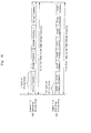
- the distribution number is made small and the number of times for driving at the same frequency increases so as not to change the burst frequency (see Fig. 10).
- changing the distribution number in accordance with the burst pulse width enables to lower the dimming level, thereby being capable of enlarging the dimming range.
- a preferable mode in the first means to solve the subjects is that the smoothing process means is configured such that an acquisition range of data to be smoothed is variable in a unit of multiple of the distribution cycle. More specifically, a detection width adjusting means is provided for calculating the data acquisition range based upon the burst pulse from the burst pulse generating means and the control timing pule from the controller (see Figs. 7 and 8). By adjusting the data acquisition range in accordance with the burst pulse width, the greater the dimming level becomes, the more the current detection accuracy enhances.
- the smoothing process means is configured to perform an averaging process (as an averaging means).
- the averaging means is preferably used for detecting with high accuracy current flowing through the cold cathode tube that is a load. It is to be noted that it may be replaced with normal filter means.so long as a strict brightness precision is especially not required.
- the controlling process means comprising the smoothing process means, error voltage calculating means, frequency setting means, frequency dividing means, controller, burst pulse generating means and output enabling means may be achieved by a hardware or a software or a hybrid configuration in combination of the hardware and software.
- a liquid crystal display device mounted thereto the cold cathode tube driving device having the above-mentioned configuration includes a liquid crystal panel, a cold cathode tube that is a backlight of the liquid crystal panel and the cold cathode tube driving device having the above-mentioned configuration, wherein the piezoelectric transformer in the cold cathode tube driving device is connected to the cold cathode tube.
- the driving pulse from the output enabling means in the cold cathode tube driving device having the above-mentioned configuration is supplied to a switching element in the power amplifying means to drive the piezoelectric transformer, to thereby control the dimming level for adjusting the brightness level of an image displayed on the liquid crystal panel.
- the burst dimming can be realized, like the first means to solve the subjects, by driving the piezoelectric transformer with a digital driving system using the frequency distribution of the driving pulse in the liquid crystal display device in which the cold cathode tube that is the backlight of the liquid crystal panel is driven by the piezoelectric transformer.
- the frequency resolution required for the necessary dimming can be obtained, whereby the current flowing though the cold cathode tube is stable even in an area where the tube current is relatively small, and hence the dimming level can be made low.
- changing the distribution number according to the burst pulse width enables to further lower the dimming level, thereby being capable of enlarging the dimming range.
- the present invention provides, as a booster transformer for driving a cold cathode tube that is a load, a cold cathode tube driving device using a piezoelectric transformer in which an output voltage varies in accordance with a frequency of an input voltage, and including a data converting means, a smoothing process means, an error voltage calculating means, a frequency setting means, a frequency dividing means, a controller, a burst pulse generating means, an output enabling means and a power amplifying means, those means being configured by the same manner as those in the first means, wherein the data converting means detects current flowing through the cold cathode tube and an input voltage of the cold cathode tube and converts the respective current values into digital data.
- the cold cathode tube driving device further includes, as new structural element, a lighting detecting means, a control cycle switching means and a dimming level switching means, those having the following functions.
- a lighting detecting means for detecting a light source
- a control cycle switching means for adjusting the brightness of the cold cathode tube driving device.
- a dimming level switching means for adjusting the brightness of the cold cathode tube driving device.
- Each means may be achieved by a software or a hardware, or a hybrid configuration in combination with a software and hardware.
- the lighting detecting means detects lighting from the output from the data converting means and applies a lighting detection pulse that is the detected result to the control cycle switching means and dimming level switching means.
- the control cycle switching means changes over the number of times A in synchronization with the lighting detection pulse outputted from the lighting detecting means and applies the same to the frequency setting means.
- the dimming level switching means performs the change-over between the externally applied dimming level and the separately set dimming level in synchronization with the lighting detection pulse outputted from the lighting detecting means, and applies the resultant level to the burst pulse generating means. By this configuration, the dimming level is controlled for adjusting the brightness level of the cold cathode tube.
- the features of the third means to solve the subjects compared to the first means are that the configuration of the data converting means is different and the lighting detecting means, control cycle switching means and dimming level switching means are newly added.
- the data converting means has a function of detecting the input voltage of the cold cathode tube in addition to the function of detecting the current flowing through the cold cathode tube.
- added in the third means are the lighting detecting means for detecting the lighting from the output from the data converting means, control cycle switching means for changing the number of times A in synchronization with the lighting detection pulse outputted from the lighting detecting means and dimming level switching means for performing the change-over between the externally applied dimming level and the separately set dimming level in synchronization with the lighting detection pulse.
- the controller controls the control cycle such that the same driving is executed predetermined number of times A (A is a natural integer not less than 2) at the same frequency like the first means to solve the subjects.
- A is a natural integer not less than 2
- Fig. 13 in an embodiment 3 described later concerning the configuration of the third means.
- the smoothing process means is illustrated as the averaging means as its one example.
- a preferable mode in the third means is that the number of times A showing the control cycle set at the control cycle switching means is set such that the number of times A at the starting is smaller than the number of times A at the lighting.
- a preferable mode in the third means is that the distribution number at the frequency dividing means is changed over in synchronization with the lighting detection pulse outputted from the lighting detecting means, and the distribution cycle at the starting is set smaller than the distribution cycle at the full lighting.
- a preferable mode in the third means is that the dimming level switching means outputs a dimming level representing 100% continuous driving when the lighting detection pulse outputted from the lighting detecting means is a value showing the non-lighting state.
- the operation of the above configuration is as follows.
- the dimming level and the burst pulse width are correlated with each other.
- the piezoelectric transformer is driven to apply a voltage to the cold cathode tube.
- the dimming level is low and the burst pulse width is narrow, the lighting performance at the starting is unsatisfactory.
- the third means is accomplished in view of this.
- the burst pulse width is set somewhat great so as to achieve a somewhat high dimming level at the dimming level switching means by the time when the lighting of the cold cathode tube is realized.
- the dimming level is set to 100% to achieve a continuous driving.
- the control cycle is set rather short at the control cycle switching means, whereby the lighting is detected within the burst pulse width at the MIN dimming. Consequently, the variation in the brightness immediately after the lighting is suppressed.
- the lighting detecting means detects the lighting and controls the control cycle switching means and dimming level switching means. The dimming level is promptly shifted to a desired dimming level after the detection of the lighting. By the multiplier effect described above, the lighting performance is satisfactory even if the dimming level is low.
- the controlling process means comprising the smoothing process means, error voltage calculating means, frequency setting means, frequency dividing means, controller, control cycle switching means, dimming level switching means, burst pulse generating means and output enabling means may be achieved by a hardware or a software or a hybrid configuration in combination of the hardware and software.
- a liquid crystal display device mounted thereto the cold cathode tube driving device having the above-mentioned configuration includes a liquid crystal panel, a cold cathode tube that is a backlight of the liquid crystal panel and the cold cathode tube driving device having the above-mentioned configuration, wherein the piezoelectric transformer in the cold cathode tube driving device is connected to the cold cathode tube. According to the liquid crystal display device, the lighting performance is satisfactory even if the dimming level of the cold cathode tube that is the backlight of the liquid crystal panel is low.
- required to the piezoelectric transformer for driving the cold cathode tube that is the backlight basically are dimming function, low electric power (high power conversion efficiency) or the like. Further, its source is battery in case where it is used in portable equipment such as a notebook-sized personal computer or a digital video camera. However, a stable source cannot be obtained by the battery source. Accordingly, stable lighting and stable power conversion efficiency within a wide power voltage range are desired considering by paying attention to the battery source.
- the present invention concerning a cold cathode tube driving device in which a power supply voltage variation is considered solves the above-mentioned subject by taking the following measures.
- the present invention of the fourth means to solve the subjects provides a cold cathode tube driving device that generates a driving pulse obtained by dividing a clock of a predetermined frequency in accordance with a frequency dividing ratio corresponding to a difference between an electric amount in a cold cathode tube that is a load of a piezoelectric transformer and a reference electric amount, and then outputs the generated pulse to the piezoelectric transformer, this device including a frequency setting means, a frequency dividing means, a power supply voltage detecting means, a pulse width calculating means and a pulse width adjusting means, each of those means having the following functions.
- Each means may be achieved by a hardware or a software, or a hybrid configuration in combination of a hardware and a software.
- the frequency setting means obtains dividing ratio information as to the driving pulse from the information of the difference, and then applies the obtained information to the frequency dividing means and pulse width cal'culating means.
- the frequency dividing means produces a distribution pulse (a driving pulse for distributing a frequency dividing ratio) that is a pulse for distributing a frequency dividing ratio based upon the dividing ratio information from the frequency setting means.
- the power supply voltage detecting means detects a power supply voltage and applies the information of the power supply voltage to the pulse width calculating means.
- the pulse width calculating means calculates information of the pulse width of the distribution pulse based upon the power supply voltage information from the power supply voltage detecting means and the dividing ratio information from the frequency setting means and applies the calculated information to the pulse width adjusting means.
- the pulse width adjusting means produces an extended pulse having a pulse width obtained by extending the pulse width of the distribution pulse based upon the pulse width information from the pulse width calculating means as well as performs a change-over between the distribution pulse and the extended pulse based upon the pulse width information and then outputs the resultant to a driving element of the piezoelectric transformer.
- Fig. 21 in an embodiment 4 described later concerning this configuration.
- the pulse width calculating means applies the pulse width information according to the detected power supply voltage to the pulse width adjusting means.
- the pulse width increases in principle as the power supply voltage lowers (see Fig. 24).
- the pulse width adjusting means produces the extended pulse from the distribution pulse, as well as selects either one of the distribution pulse and the extended pulse based upon. the pulse width information, i.e., the detected power supply voltage, and then outputs the selected one to the driving element of the piezoelectric transformer.
- the production of the extended pulse from the distribution pulse is digitally executed.
- a pulse obtained by shifting the timing of the distribution pulse is produced.
- the pulse having the shifted timing is composed with the initial distribution pulse by taking a logical sum, resulting in producing the extended pulse having a width greater than that of the distribution pulse.
- the extended pulse has a pulse width extended by a period of the shifted timing. How much to shift the timing is determined based upon the pulse width information corresponding to the detected power supply voltage. Further, which one is selected from the initial distribution pulse and the extended pulse is also determined based upon the pulse width information. By this process, the driving pulse having a pulse width corresponding to the detected power supply voltage can digitally be realized to be produced.
- the period of shift is set as smaller as possible.
- This configuration can provide a driving pulse having an optimum pulse width in a wide power supply voltage range even in a digital driving system.
- the resolution of the pulse width can be made twice that of the distribution pulse. This leads to reduce a power consumption due to an improvement in efficiency and to prevent a break-down of an FET or piezoelectric transformer because of a surge upon driving the piezoelectric transformer, thereby bringing a great effect.
- the pulse width calculating means is configured to output the pulse width information obtained from the power supply voltage information from the power supply voltage detecting means and the dividing ratio information from the frequency setting means as data including decimal means corresponding to one cycle or less of a clock.
- the pulse width adjusting means is configured to include a pulse width shaping means, a pulse width extending means and a switching means.
- the pulse width shaping means shapes the pulse width of the distribution pulse outputted from the frequency dividing means into a value corresponding to an integer means of the pulse width information.
- the pulse width extending means converts the output from the pulse width shaping means into the extended pulse having an extended pulse width.
- One or more pulse width extending means are provided.
- the switching means performs a change-over between the output from the pulse width extending means and the output from the pulse width shaping means in accordance with the value of the decimal means of the pulse width information and outputs the resultant.
- the distribution number is defined by the number of the initial distribution pulses existing in one distribution cycle. This distribution number is a natural number.
- the pulse width is adjusted only by adjusting the distribution number, all the adjustment that can be made is only by the natural number unit. Specifically, the pulse width next greater than the distribution number N is (N + 1), while the pulse width next smaller than the distribution pulse is (N - 1).
- the present measure is to adjust the pulse width at a level of the tenth's place, not by the natural number unit.
- the present invention having the above-mentioned configuration can be described as follows by illustrating from another angle of view.
- the present invention of the fourth means to solve the subjects provides a cold cathode tube driving device that generates a driving pulse obtained by dividing a clock of a predetermined frequency in accordance with a frequency.
- the frequency setting means obtains dividing ratio information as to the driving pulse from the information of the difference.
- the frequency dividing means produces a distribution pulse having a dividing ratio of D + 1 L times (L > K) during K cycles of the driving pulse with respect to the reference dividing ratio D.
- the power supply voltage detecting means detects an inputted power supply voltage.
- the pulse width calculating means outputs the pulse width information obtained from the power supply voltage information from the power supply voltage detecting means and the dividing ratio information from the frequency setting means as data including decimal means corresponding to one cycle or less of a clock.
- the pulse width shaping means shapes the pulse width of the distribution pulse outputted from the frequency dividing means into a value corresponding to an integer means of the pulse width information.
- the pulse width extending means converts the output from the pulse width shaping means into the extended pulse having an extended pulse width. One or more pulse width extending means are provided.
- the switching means performs a change-over between the output from the pulse width extending means and the output from the pulse width shaping means in accordance with the value of the decimal means of the pulse width information and outputs the resultant to a driving element of the piezoelectric transformer.
- Fig. 28 in the embodiment 4 described later concerning this configuration.
- the pulse width extending means includes a delay fine-adjusting means that converts the output from the pulse width shaping means into an extended pulse having a pulse width extended with the respective delay difference set shorter than one cycle of the clock.
- a preferable mode in the above configuration is that the delay fine-adjusting means is configured by a flip-flop that latches at a trailing edge of a clock.
- the delay fine-adjusting means is configured by a flip-flop that latches at a trailing edge of a clock.
- a pulse width resolution with a double precision by using a trailing edge of a clock can be obtained without deviating from a designing technique of a digital LSI.
- a fifth means to solve the subjects solves the above-mentioned subject by taking the following measures in a cold cathode tube driving device in which a power supply voltage variation is considered.
- the present invention of the fifth means to solve the subjects provides a cold cathode tube driving device that generates a driving pulse obtained by dividing a clock of a predetermined frequency in accordance with a frequency dividing ratio corresponding to a difference between an electric amount in a cold cathode tube that is a load of a piezoelectric transformer and a reference electric amount, and then outputs the generated pulse to the piezoelectric transformer, this device including a frequency setting means, a frequency dividing means, a power supply voltage detecting means, a pulse width calculating means and a pulse width adjusting means, each of those means having the following functions.
- Each means may be achieved by a hardware or a software, or a hybrid configuration in combination of a hardware and a software.
- the frequency setting means obtains dividing ratio information as to the driving pulse from the information of the difference, and then applies the obtained information to the frequency dividing means and pulse width calculating means.
- the frequency dividing means produces a distribution pulse (a driving pulse for distributing a frequency dividing ratio) that is a pulse for distributing a frequency dividing ratio based upon the dividing ratio information from the frequency setting means, and applies the produced pulse to the pulse width adjusting means.
- the power supply voltage detecting means detects a power supply voltage and applies the information of the power supply voltage to the pulse width calculating means.
- the pulse width calculating means calculates information of the pulse width of the distribution pulse based upon the power supply voltage information from the power supply voltage detecting means and the dividing ratio information from the frequency setting means and applies the calculated information to the pulse width adjusting means.
- the pulse width adjusting means produces an extended pulse having a pulse width obtained by extending the pulse width of the distribution pulse by 0.5 cycles, produces a delayed pulse and delayed and extended pulse each having a pulse width obtained by respectively delaying the distribution pulse and extended pulse by 0.5 cycles based upon the pulse width information from the pulse width calculating means, performs a change-over among the distribution pulse, extended pulse, delayed pulse and delayed and extended pulse based upon the pulse width information, and then, outputs the resultant to a driving element of the piezoelectric transformer.
- Fig. 30 in an embodiment 5 described later concerning this configuration.
- the difference from the fourth means lies in the pulse width adjusting means.
- the pulse width adjusting means in the fifth means produces pulses of three types from the distribution pulse and selects one pulse among pulses of four types in total. Four types are (1) distribution pulse, (2) extended pulse having a pulse width obtained by extending the pulse width of the distribution pulse, (3) delayed pulse obtained by delaying the distribution pulse and (4) delayed and extended pulse obtained by delaying the extended pulse.
- the cold cathode tube driving device of this embodiment can finely adjust the pulse width of the driving pulse by effectively using the trailing edge of a clock without hindering the effect of this case, to thereby obtain an optimum pulse width in accordance with a power supply voltage.
- a double resolution i.e., a resolution having precision four times that of the distribution pulse in total can be obtained compared to the fourth means, whereby a pulse width control with higher precision can be obtained (see Fig. 31).
- An effect in power consumption and effect for preventing a break-down due to a surge because of the other improvements in efficiency can similarly be obtained.
- the pulse width calculating means is configured to output the pulse width information obtained from the power supply voltage information from the power supply voltage detecting means and the dividing ratio information from the frequency setting means as data including decimal means corresponding to one cycle or less of a clock.
- the pulse width adjusting means is configured to include a pulse width shaping means, a 1-clock-cycle delaying means, a 0.5-clock-cycle delaying means and a switching means.
- the pulse width shaping means shapes the pulse width of the distribution pulse outputted from the frequency dividing means into a value corresponding to an integer means of the pulse width information.
- the 1-clock-cycle delaying means latches the output from the pulse width shaping means at the leading edge of a clock.
- the 0.5-clock-cycle delaying means latches the output from the pulse width shaping means at the trailing edge of a clock for producing a delay pulse.
- An extended pulse is formed by taking a logical sum (first logical sum) of the delay pulse that is the output from the 0.5-clock-cycle delaying means and the distribution pulse that is the output from the pulse width adjusting means, while a delayed and extended pulse is formed by taking a logical sum (second logical sum) of the delay pulse that is the output from the 0.5-clock-cycle delaying means and the extended pulse that is the output from the 1-clock-cycle delaying means.
- the switching means outputs each pulse obtained in the following four patterns as a driving pulse to the driving element of the piezoelectric transformer.
- the present invention having the above-mentioned configuration can be described as follows by illustrating from another angle of view.
- the present invention of the fifth means to solve the subjects provides a cold cathode tube driving device that generates a driving pulse obtained by dividing a clock of a predetermined frequency in accordance with a frequency dividing ratio corresponding to a difference between an electric amount in a cold cathode tube that is a load of a piezoelectric transformer and a reference electric amount, and then outputs the generated pulse to the piezoelectric transformer, this device including a frequency setting means, a frequency dividing means, a power supply voltage detecting means, a pulse width calculating means, a pulse width shaping means, a 1-clock-cycle delaying means, a 0.5-clock-cycle delaying means, a pulse width extending means and a switching means, each of those means having the following functions.
- the frequency setting means obtains dividing ratio information as to the driving pulse from the information of the difference.
- the frequency dividing means produces a distribution pulse having a dividing ratio of D+1 L times (L ⁇ K) during K cycles of the driving pulse with respect to the reference dividing ratio D.
- the power supply voltage detecting means detects an inputted power supply voltage.
- the pulse width calculating means outputs the pulse width information obtained from the power supply voltage information from the power supply voltage detecting means and the dividing ratio information from the frequency setting means as data including decimal means corresponding to one cycle or less of a clock.
- the pulse width shaping means shapes the pulse width of the distribution pulse outputted from the frequency dividing means into a value corresponding to an integer means of the pulse width information.
- the 1-clock-cycle delaying means latches the output from the pulse width shaping means at the leading edge of a clock.
- the 0.5-clock-cycle delaying means latches the output from the pulse width shaping means at the trailing edge of a clock.
- the switching means is configured to have the following functions.
- the switching means is configured as described above.
- Sixth means to solve the subjects solves the above-mentioned subject by taking the following measures in a cold cathode tube driving device in which a power supply voltage variation is considered.
- the present invention of the sixth means to solve the subjects provides a cold cathode tube driving device that generates a driving pulse obtained by dividing a clock of a predetermined frequency in accordance with a frequency dividing ratio corresponding to a difference between an electric amount in a cold cathode tube that is a load of a piezoelectric transformer and a reference electric amount, and then outputs the generated pulse to the piezoelectric transformer, this device including a frequency setting means, a frequency dividing means, a power supply voltage detecting means, a pulse width calculating means, a pulse width distributing means and a pulse width adjusting means, each of those means having the following functions.
- Each means may be achieved by a hardware or a software, or a hybrid configuration in combination of a hardware and a software.
- the frequency setting means obtains dividing ratio information as to the driving pulse from the information of the difference, and then applies the obtained information to the frequency dividing means and pulse width calculating means.
- the frequency dividing means produces a distribution pulse (a driving pulse for distributing a frequency dividing ratio) that is a pulse for distributing a frequency dividing ratio based upon the dividing ratio information from the frequency setting means, and applies the produced pulse to the pulse width adjusting means.
- the power supply voltage detecting means detects a power supply voltage and applies the information of the power supply voltage to the pulse width calculating means.
- the pulse width calculating means calculates information of the pulse width of the distribution pulse based upon the power supply voltage information from the power supply voltage detecting means and the dividing ratio information from the frequency setting means and applies the calculated information to the pulse width distributing means.
- the pulse width distributing means inputs the pulse width information from the pulse width calculating means, increases the pulse width information at a predetermined timing and then outputs the resultant to the pulse width calculating means.
- the pulse width adjusting means adjusts the pulse width of the distribution pulse from the frequency dividing means according to the output from the pulse width distributing means and outputs the resultant to the driving element of the piezoelectric transformer. Reference is made to Fig. 33 in an embodiment 6 described later concerning this configuration.
- the sixth means provides a system in which the pulse width is distributed at a predetermined cycle for obtaining a resolution of a pulse duty at an average pulse width in a driving pulse during a predetermined cycle, to thereby be capable of obtaining a pulse width adjustment with highly enhanced resolution compared to the fourth means and fifth means described above.
- This system enables to perform a smooth duty control with respect to a power supply voltage, thereby improving a driving efficiency of the piezoelectric transformer. This greatly contributes to power reduction at a backlight means. Further, this system can be used in synchronization with the distribution in the frequency dividing ratio, thereby not ruining the conventional effect. Additionally, it can be used with the above-mentioned fourth means and fifth means. The combination of these systems is very effective for improving efficiency.
- a preferable mode in the sixth means to solve the subjects is that the pulse width calculating means is configured to output the pulse width information as A-bit data based upon the power supply voltage information and the dividing ratio information obtained at the frequency dividing means, and that the pulse width distributing means is configured to output data obtained by adding 1 to the high-order (A - n)-bit data of the A-bit pulse width information during nth root of 2 of the distribution pulse the times represented by the low-order n-bit of the A-bit pulse width information.
- the present invention of the sixth means having the above-mentioned configuration can be described as follows by illustrating from another angle of view.
- the present invention of the sixth means to solve the subjects provides a cold cathode tube driving device that generates a driving pulse obtained by dividing a clock of a predetermined frequency in accordance with a frequency dividing ratio corresponding to a difference between an electric amount in a cold cathode tube that is a load of a piezoelectric transformer and a reference electric amount, and then outputs the generated pulse to the piezoelectric transformer, this device including a frequency setting means for obtaining dividing ratio information as to the driving pulse from the information of the difference, a frequency dividing means that produces a distribution pulse having a dividing ratio of D + 1 L times (L ⁇ K) during K cycles of the driving pulse with respect to the reference dividing ratio D, a power supply voltage detecting means that detects an inputted power supply voltage, a pulse width calculating means that outputs the pulse width information as A-bit data based upon the power
- the pulse width distributing means is configured to distribute a distribution pulse such that the duty ratio of the pulse width of the distribution pulse becomes approximately constant
- the frequency dividing means is configured to include a frequency dividing means that divides a clock having a predetermined frequency with the dividing ratio D illustrated by high-order (M - n)-bit data of the M-bit dividing ratio information in order to make the duty ratio of the pulse width of the distribution pulse approximately constant and a dividing ratio distributing means that outputs 1 during nth root of 2 of the distribution pulse the times represented by the low-order n-bit of the M-bit dividing ratio information to make the dividing ratio of the frequency dividing means D + 1, wherein the pulse width distributing means is configured to add 1 to the high-order (A - n)-bit data of the A-bit pulse width information when the output from the dividing ratio distributing means is 1.
- An adder 110 in Fig. 33 concerning this configuration.
- the cold cathode tube driving device may also include, in front of the frequency setting means, a current detecting means for detecting a current flowing through the cold cathode tube that is a load of the piezoelectric transformer, a rectifying means that converts a sinusoidal voltage obtained from the current detecting means into an approximately DC voltage, an A/D converter that converts the rectified voltage signal into a digital signal, a smoothing process means for smoothing the output data from the A/D converter and an error voltage calculating means that multiplies difference data between the externally applied reference data and the output data from the smoothing process means by a constant and outputs the resultant to the frequency setting means as error data.
- a current detecting means for detecting a current flowing through the cold cathode tube that is a load of the piezoelectric transformer
- a rectifying means that converts a sinusoidal voltage obtained from the current detecting means into an approximately DC voltage
- an A/D converter that converts the rectified voltage signal into a digital signal
- Fig. 1 is a block diagram showing a schematic configuration of the liquid crystal display device having mounted thereto a cold cathode tube driving device.
- numeral 100 denotes a liquid crystal panel displaying an image
- 200 a backlight device (including a cold cathode tube 210) with respect to the liquid crystal panel 100
- 300 a liquid crystal driving device that converts an inputted imaging signal into a liquid crystal driving signal and outputs dimming data for controlling a brightness of the backlight device 200 in synchronization with the imaging signal
- 400 a backlight driving controller for driving the backlight 400 and controlling the dimming (hereinafter referred to as a driving controller), 500 a power amplifier for power-amplifying a driving pulse outputted from the driving controller 400, 600 a piezoelectric transformer that drives the cold cathode tube 210 in the backlight device 200 based upon the driving pulse from the power amplifier 500, 700 a data converter that electrically detects the driving state of the cold cathode tube 210 in the backlight device 700 and
- the present invention is structured such that the driving controller 400 is realized in a digital form for making the one-chip LSI incorporating the liquid crystal driving device 300 and the driving controller 400, thereby enabling a backlight dimming in synchronization with the image and realizing reduced cost and saved space.
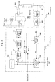
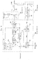
- Fig. 2 is a block diagram showing a configuration of the cold cathode tube driving device 900 in the liquid crystal display device according to the embodiment 1 of the invention.
- numeral 1 denotes a piezoelectric transformer (corresponding to the piezoelectric transformer 600 in Fig.
- the current detector 5 is typically represented by a mark of a resistance in the figure, it is not limited to the resistance.
- the A/D converter 101 has a sufficient number of bits in order to obtain a voltage detection accuracy and its sampling clock has a frequency sufficient for assuring a response speed required for the control.
- An output digital signal from the A/D converter 101 is represented by Vad.
- Numeral 102 denotes an averaging means (preferable example of smoothing process means) that performs an averaging process to a detection voltage Vad outputted from the A/D converter 101 within a predetermined sample number N (described later).
- the output digital signal from the averaging means 102 is represented by Vave hereinafter.
- Numeral 103 denotes an error voltage calculating means that compares the output signal Vave from the averaging means 102 with externally set reference data Vref, calculates the difference between them and outputs the resultant as error data Verr.
- Numeral 104 denotes a frequency setting means for setting a frequency of a driving pulse of the piezoelectric transformer 1. This frequency setting means 104 adds or subtracts the frequency corresponding to the error data Verr to or from the previous frequency setting value Fprev, and outputs M-bit data Fnext.
- This data Fnext means a frequency dividing ratio for the N cycle of the driving pulse. Specifically, the value of Fnext/N becomes an average frequency dividing ratio Div of the driving pulse for N cycle.
- Numeral 121 denotes a controller for generating a control timing pulse at a predetermined period based upon the frequency data Fnext outputted from the frequency setting means 104. This control period is set to the period A (A: natural integer) times the N cycle of the driving pulse. A burst frequency has a period equal to that of the timing pulse outputted from the controller 121.
- Numeral 105 denotes a frequency dividing means that distributes the frequency dividing ratio such that the average frequency dividing ratio Div of the driving pulse for N cycle becomes Fnext/N to divide a clock.
- a driving pulse to the piezoelectric transformer 1 is produced by the frequency dividing means 105.
- the cycle comprising the driving pulse for N cycle is a distribution cycle.
- Numeral 122 denotes a burst pulse generating means that outputs a pulse (hereinafter referred to as a burst pulse) having a duty ratio corresponding to a dimming level included in the dimming data applied from an external means (the liquid crystal driving device 300 in Fig. 1) based upon the control cycle pulse obtained at the controller 121.
- This burst pulse is set such that "H" level period is not shorter than the distribution cycle.
- Numeral 123 denotes an output enabling means that switches over the enabling and disabling of the output of the driving pulse obtained at the frequency dividing means 105. It is configured to be disabled to stop the driving when the value of the burst pulse is "L" level.
- the sampling number at the averaging means 102 is set to be equal to the sampling number during the period of the distribution cycle.
- the corresponding relationship between Fig. 1 and Fig. 2 is as follows.
- the coil 2 and the FET 3 constitute the power amplifier 500 that power-amplifies the driving pulse outputted from the output enabling means 123 and outputs the resultant to the piezoelectric transformer 1.
- the current detector 5, rectifying means 7 and A/D converter 101 constitute the data converter that converts the current flowing through the cold cathode tube 4 into digital data.
- the averaging means 102, error voltage calculating means 103, frequency setting means 104, controller 121, frequency dividing means 105, burst pulse generating means 122 and output enabling means 123 constitute the driving controller 400 that is made by a digital circuit.
- This driving controller 400 produces a driving pulse that is to be applied to the piezoelectric transformer 1 based upon the current information in the cold cathode tube 4 outputted from the data converter 700 and the externally inputted dimming level and the reference data, to thereby control the luminous amount of the cold cathode tube 4.
- the first feature of the present embodiment is that the control cycle is A (A: natural integer) times N cycle of the driving pulse (the distribution cycle) for driving A times at the same average frequency, and the burst pulse width is set such that its "H" level period is not shorter than the distribution cycle.
- the second feature is that the sampling number N of the averaging means 102 is set to be equal to the sampling number during the period of the distribution cycle. What is meant by these two features will be explained with reference to Fig. 3.
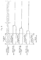
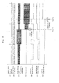
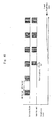
- Fig. 3 is a timing chart for explaining an operational concept of the embodiment 1.
- Fig. 3 (A) shows the control cycle pulse outputted from the controller 121
- Fig. 3(B) shows the driving pulse (substantially shown in Fig. 4 (C) ) outputted from the frequency dividing means 105
- Fig. 3(C) shows the burst pulse (by which the on-duty is determined during the control cycle) outputted from the burst pulse generating means 122
- Fig. 3 (D) shows the driving pulse outputted from the output enabling means 123
- Fig. 3 (E) shows the tube current flowing through the cold cathode tube 4
- Fig. 3(F) shows the current detection signal outputted from the rectifying means 7, Fig.
- FIG. 3(G) shows the data range in which the averaging process is performed at the averaging means 102 and Fig. 3 (H) shows the output data Vave from the averaging means 102.
- the value of A is set to 4.
- the frequency dividing means 105 gets high-precise frequency resolution at the average frequency for the driving pulse N cycle. Therefore, the piezoelectric transformer 1 is driven with the driving pulse obtained at the frequency dividing means 105. Hence, in case where the current flowing through the cold cathode tube 4 is detected, the detection has to be made per this distribution cycle unit.
- control is performed to make the current during ON-period constant upon the burst driving.
- the burst pulse width becomes shorter than the distribution cycle, so that the current during the ON-period cannot be controlled to be constant. Therefore, as shown in Fig. 3(A), driving is performed plural times (plural distribution cycles) at the same average frequency and the burst pulse width (ON-period) is set so as not to be shorter than one distribution cycle, to thereby assure a period for detecting average current during one distribution cycle.
- the system of the present invention does not detect current during "H"-level period (ON-period) of the burst pulse like the system disclosed in the document 2, but detects the current only during "H"-level period of the burst pulse as well as during the first distribution cycle period (the first cycle of four distribution cycles) as shown in Fig. 3(G).
- the resolution of the A/D converter is set to 3-bit and the aimed tube current value is 6.5 obtained by the conversion of the digital data outputted from the A/D converter 101.
- Decimal fraction data is not outputted from the A/D converter 101.
- decimal fraction exists.
- the frequency data Fnext outputted from the frequency setting means 104 is 10110.
- the high-order 3-bit represents the integer means and.low-order 2-bit represents the decimal fraction means. Since the distribution cycle N is set to 4, the decimal fraction means is 2-bit.
- the driving pulse shown in Fig. 4(C) is outputted from the frequency dividing means 105.
- driving pulses of four cycles are illustrated in one distribution cycle, that is the distribution cycle N.
- Fig. 4 (E) shows the tube current waveform when the burst pulse is applied. As shown in Fig. 4(E), the current value becomes a value corresponding to the frequency of the driving pulse.
- Fig. 4(F) shows an output waveform obtained at the rectifying means 7 with the peak detection after detecting the tube current by the current detector 5.
- the A/D output data during the distribution cycle is obtained such as "4", "5", "4", "5" as shown in Fig. 4(G).
- the average current upon ON-period changes depending strictly upon the burst pulse width, that will be explained with reference to Fig. 5.
- Fig. 5(A) shows a distribution example of the frequency dividing ratio. The current according to the frequency dividing ratio flows through the cold cathode tube 4. The current detection period in this example is only the first distribution cycle as shown in Fig. 5, and the average frequency dividing ratio during this cycle is 4.5.
- the brightness is greatly influenced by the dimming precision due to the burst pulse width.
- the frequency dividing ratio is actually far greater than 4 or 5.
- a pulse of 100 KHz is produced with a clock of 10 MHz, for example, a clock is required to be divided by 100.
- the frequency dividing ratio is far greater than 4 (e.g., 256 distributions). Therefore, the error by the detection becomes a level that can nearly be ignored.
- the control cycle is A times (A: natural integer) N cycle of the driving pulse (distribution cycle) for driving A times at the same average frequency, and the sampling number N at the averaging means 102 becomes equal to the sampling number during the distribution cycle. Therefore, the burst dimming can be realized in the digital driving system using the frequency distribution of the driving pulse. Consequently, the present invention can provide a cold cathode tube driving device using a digital system that is advantageous in reducing cost and saving space because of one-chip formation with the other LSIs, to thereby bring a great effect to a further miniaturization of a small-sized imaging equipment.
- the current detection period is set to the first distribution cycle in this embodiment, the current detection period is not limited to this cycle. This is because the cold cathode tube 4 does not always start lighting immediately after the voltage is applied thereto. Specifically, some delay occurs upon starting the lighting. Upon the burst driving, the tube current starts to flow after a short time after the shift from OFF to ON as shown in Fig. 6(E). Therefore, if the current detection period is set to the first distribution cycle, accurate average current cannot be detected, thus disadvantageous. In view of this, the detected position may be shifted without changing the detected width considering the delay time occurred from restarting the driving to the lighting as shown in Fig. 6(F).
- this current detection period is not necessarily set to one distribution cycle.
- the current detection period may be varied to have a width of the double of the distribution cycle or a width of the triple of the distribution cycle or the like in accordance with the burst pulse width as shown in Fig. 7.
- a block diagram of this case is shown in Fig. 8.
- numeral 124 denotes a detection width adjusting means that calculates a detection range from the burst pulse from the burst pulse generating means 122 and the control timing pulse from the controller 121 for adjusting the detection range in accordance with the burst pulse width.
- a normal filter can be replaced with the averaging means in case where a strict brightness precision is not required.
- the averaging means or filter means can collectively be referred to as smoothing process means. They are referred to as smoothing process means in claims of the invention.
- each element constituting the driving controller 400 such as the averaging means 102, error voltage calculating means 103, controller 121, frequency setting means 104, burst pulse generating means 122, frequency dividing means 105, output enabling means 123 and detection width adjusting means 124 may be achieved by a hardware or software or by a hybrid structure in combination with a hardware and software.
- a cold cathode tube driving device according to the embodiment 2 of the invention.
- the detection range for a minimum of one distribution cycle is required.
- the burst pulse width is required to be greater than the distribution cycle and there is a restriction for the lower limit of the dimming level.
- the embodiment 2 solves this subject.
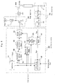
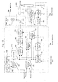
- Fig. 9 is a block diagram showing a configuration of a cold cathode tube driving device according to the embodiment 2.
- Numeral 104a denotes a frequency setting means for setting a frequency of a driving pulse of the piezoelectric transformer 1.
- This frequency setting means 104a adds or subtracts the frequency corresponding to the error data Verr to or from the previous frequency setting value Fprev, and outputs M-bit data Fnext.
- the different point from the frequency setting means 104 explained in the embodiment 1 shown in Fig. 2 is that, among the M-bit data showing the frequency dividing ratio including the decimal fraction, the effective bit number in the decimal fraction means is variable in the embodiment 2 while it is fixed in the embodiment 1.
- Numeral 121a denotes a controller for generating a control timing pulse at a predetermined period based upon the frequency data Fnext outputted from the frequency setting means 104a.
- This control period is set to the period A x k times (A is a natural integer, and k is a value varying in accordance with the distribution cycle) the N cycle of the driving pulse.
- Numeral 105a denotes a frequency dividing means that distributes the frequency dividing ratio such that the average frequency dividing ratio Div of the driving pulse for N cycle becomes Fnext/N to divide a clock.
- the driving pulse of the piezoelectric transformer 1 is produced by the frequency dividing means.
- the different point from the frequency dividing means 104a in the embodiment 1 shown in Fig. 2 is that the value N determining the distribution cycle can be set from outside of the frequency dividing means.
- Numeral 125 denotes a distribution number adjusting means that determines the distribution number from the burst pulse width outputted from the burst pulse generating means 122 and then outputs the distribution number N to the frequency dividing means 105a as well as outputs a change-over signal to the frequency setting means 104a. Further, it sets a value of k to the controller 121a. The value of k is determined such that the value (k x N) is made constant so as not to change the control frequency even if the distribution number N changes.
- the other configurations are the same as those in the embodiment 1 shown in Fig. 2, so that the explanation thereof is omitted here.
- the feature of the present embodiment is that the distribution number N varies (i.e., the distribution cycle varies) in accordance with the burst pulse width, and the number of driving at the same average frequency is simultaneously changed so as not to change the control cycle (i.e., burst pulse cycle) even if the distribution cycle changes.
- Fig. 10(A) shows that the frequency dividing ratio is distributed so as to obtain an average frequency accuracy at N cycle of the driving pulse. In this case, driving is performed four times at the same average frequency.
- Fig. 10 (B) shows that the frequency dividing ratio is distributed so as to obtain an average frequency accuracy at N/2 cycle of the driving pulse. In this case, driving is performed eight times at the same average frequency to achieve the same control cycle as the case shown in Fig. 10(A).
- the detection range for a minimum of one distribution cycle is required as explained in the embodiment 1.
- a minimum of 25% of the burst pulse duty is required to assure the detection during one distribution cycle, while 12.5 % is enough in the case of Fig. 10(B).
- the current accuracy is higher as the distribution number is great, so that the current accuracy in Fig. 10(B) is half that in Fig. 10(A).
- a low brightness means does not require the dimming precision compared to a high brightness means.
- a low brightness mode is used to reduce power consumption when only a stand-by mode or OSD (on-screen display) is displayed. In the case of the low brightness (in case where the burst pulse width is not more than the predetermined value) , the distribution number is made small and the number of times for driving with the same frequency increases so as not to change the burst frequency.
- Fig. 12 shows the embodiment of this case.
- numeral 121b denotes a controller configured such that the number of times A driven at the same frequency can be set from outside of the controller and numeral 126 denotes a control cycle setting means that sets the driving times A of the controller 121b in synchronization with the burst pulse. It increases the amount of A to lower the MIN dimming level in case where the dimming level reaches not more than the predetermined level.
- the configuration shown in Fig. 12 brings an effect of greatly enlarging the detection range compared to the embodiment 1, although the burst frequency (ON/OFF frequency) varies.
- the present embodiment may adopt a means for changing the detection range according to the duty of the burst pulse or adopt the replacement of the averaging means with a simple filter means as explained in the embodiment 1.
- each element constituting the driving controller 400 such as the averaging means 102, error voltage calculating means 103, controller 121, frequency setting means 104a, burst pulse generating means 122, frequency dividing means 105a, output enabling means 123, distribution number adjusting means 125 and control cycle setting means 126 may be achieved by a hardware or software or by a hybrid structure in combination with a hardware and software.
- Fig. 13 shows a block diagram showing a configuration of the cold cathode tube driving device according to the embodiment 3 of the invention.
- This embodiment provides a cold cathode tube driving device that does not deteriorate a lighting performance and lighting quality at the starting even if the dimming level is low.
- numeral 14 denotes voltage detecting means for detecting an output voltage from the piezoelectric transformer 1, and 15 a shielding means for turning on or off the detected voltage of the piezoelectric transformer 1 detected by the voltage detecting means 14.
- the shielding means is configured such that the output voltage therefrom becomes at "L" level when the detected voltage is turned off.
- Numeral 7a denotes a peak detecting means for detecting the output voltage of the piezoelectric transformer 1 outputted from the shielding means 15 and the maximum tube current outputted from the current detector 5.
- the current detector 5, peak detecting means 7a, voltage detecting means 14, shielding means 15 and A/D converter 101 constitute a data converter 700a that time-sharingly detects the current flowing through the cold cathode tube 4 and the output voltage of the piezoelectric transformer 1 and converts the resultant into digital data.
- Numeral 127 denotes a lighting detecting means for performing a lighting detection from the digital output data from the A/D converter 101. It executes ON/OFF control of the shielding means 15 at a predetermined period for performing the lighting detection.
- the lighting detecting means 127 is configured to output a detection switching pulse to the shielding means 15 and output a lighting detection pulse to a dimming level switching means 128 and a control cycle switching means 129 described later. This lighting detecting means 127 will be explained later in detail.
- Numeral 128 denotes the dimming level switching means for changing over the dimming level applied to the burst pulse generating means 122 based upon the lighting detection pulse outputted from the lighting detecting means 127. It is configured to output the previously set dimming level at the starting. It is to be noted here that the dimming level at the starting is 100% (continuous driving).
- Numeral 121b denotes a controller that can set the number of times A for driving at the same frequency from the outside. This controller is same as that shown in Fig. 12.
- Numeral 126a denotes a first control cycle setting means for setting a first control cycle of the controller 121b
- numeral 126b denotes a second control cycle setting means for setting a second control cycle of the controller 121b.
- Numeral 129 denotes the control cycle switching means that performs a change-over between control cycle information outputted from the first control cycle setting means 126a and control cycle information outputted from the second control cycle setting means 12 6b based upon the lighting detection pulse outputted from the lighting detecting means 127, and outputs the resultant.
- the first control cycle setting means 126a sets the control cycle at the starting.
- the control cycle set by the first control setting means 126a is set to correspond to two distribution cycles (the amount of A is 2).
- the second control cycle setting means 126b sets the control cycle at the lighting. Its cycle is set to correspond to four distribution cycles (the amount of A is 4) like the embodiment 1.
- the other configurations are the same as those in the embodiment 1 explained by using Fig. 2, so that their explanations are omitted here.
- a driving controller 400c is configured by the averaging means 102, error voltage calculating means 103, frequency setting means 104, controller 121b, frequency dividing means 105, burst pulse generating means 122, output enabling means 123, lighting detecting means 127, dimming level switching means 128, first control cycle setting means 126a, second control cycle setting means 126b and control cycle switching means 129, those of which are configured as described above.
- control cycle is changed over between at the starting and at the lighting, and the control cycle at the starting is made shorter.
- Fig. 14 shows control cycles at the starting and lighting.
- Fig. 14 (A) shows a driving pulse during one control cycle at the starting, i.e., driving is performed two times at the same average frequency.
- Fig. 14(C) shows a driving pulse during one control cycle at the lighting, i.e., driving is performed four times at the same average frequency.
- Fig. 14 (B) shows a voltage (current) detection period at the starting. The detection is made with the delay A shifted.
- Fig. 14 (D) shows a voltage (current) detection period at the lighting. The detection is made with the delay A shifted like the case at the starting.
- Fig. 15 shows the operation of the lighting detecting means 127 at the starting.
- Fig. 15 (C) shows an output voltage detection signal of the piezoelectric transformer 1 outputted from the voltage detecting means 14, while Fig. 15 (D) shows a current detection signal outputted from the current detector 5.
- the current does not flow at the starting since the cold cathode tube 4 is not lit.
- the control cycle setting means 129 selects the first control cycle setting means 126a, so that the control cycle corresponding to two same driving periods is set.
- the dimming level switching means 128 selects the dimming level of the continuous driving and outputs the selected resultant to the burst pulse generating means 122.
- Fig. 15 (E) shows a change-over pulse that is a detection pulse outputted to the shielding means 15 from the lighting detecting means 127 for detecting the lighting.
- this change-over pulse is at "H” level
- the shielding means is turned OFF, and a peak value of the current detection signal is outputted from the peak detecting means 7a.
- the detection of the lighting is determined by the output level of the peak detecting means 7a when the change-over pulse is at "H” level.
- the output from the peak detecting means 7a is at zero level at the non-lighting period since the tube current does not flow, while the tube current flows when the lighting is started, so that the voltage corresponding to the tube current is outputted from the peak detecting means 7a.
- the change-over pulse is at "H” level
- the lighting is not executed when the output from the peak detecting means 7a is at "L” level, while the lighting is determined to be performed when the output from the peak detecting means 7a is not less than the predetermined level.
- Fig. 15 the lighting is started at a time T1, whereupon the tube current starts to flow as shown in Fig. 15 (D).
- the output from the peak detecting means 7a becomes to a level correspond to the tube current when the change-over pulse shown in Fig. 15 (E) is at "H” level, whereby the lighting is detected.
- the lighting detection pulse shown in Fig. 15(G) shifts from "L" level to "H” level.
- Fig. 16 shows each waveform when the control at the starting is shifted to the control at the lighting.
- the cold cathode tube 4 starts to light at the time T1, so that the tube current starts to flow.
- the lighting is detected by the change-over pulse, whereby the lighting detection pulse shifts from "L" level to "H” level.
- the control cycle switching means 129 is switched to a state for selecting the second control cycle setting means 126b. By this, the control cycle is changed from the cycle corresponding to two same driving periods to that corresponding to four same driving periods. Simultaneously, the dimming level switching means 128 changes the dimming level for the continuous driving to the externally applied dimming level, and outputs the resultant to the burst pulse generating means 122. By this operation, the burst pulse is outputted from the time T2 as shown in Fig. 16 (H) , to thereby change the dimming to the burst dimming.
- the control cycle at the lighting period is not actually 4.
- the burst frequency is 150 Hz
- the driving frequency of the piezoelectric transformer 1 is 150 KHz and the distribution number is 100
- the control cycle becomes ten times the distribution cycle.
- the maximum irregular period is 20% of the control cycle at the lighting period as shown in Fig. 17. The change in the brightness level at this time can actually be neglected.
- Fig. 18 shows this example.
- numeral 125a denotes a distribution number adjusting means for performing the change-over of the distribution cycle from the frequency setting means 104a.
- the frequency setting means 104a performs the same operation as the frequency setting means shown in Fig. 9 in the embodiment 2. Specifically, the distribution number changes depending upon the output from the distribution number adjusting means 125a. The different point from the distribution adjustment means 125 shown in Fig.
- the distribution number adjusting means 125a in this embodiment is configured to change the distribution number between at the lighting and at the starting, while the distribution number adjusting means 125 in the embodiment 2 changes the distribution number in accordance with the burst pulse width from the burst pulse generating means 122, i.e., in accordance with the dimming level. Therefore, the lighting detection pulse from the lighting detecting means 127 is inputted to the distribution number adjusting means 125a.
- the other operations are the same as those shown in Fig. 13.
- Fig. 19 shows each waveform of each means from the starting to the lighting.
- the lighting detection period in this embodiment at the starting is one half the period in the embodiment shown in Fig. 13, whereby the irregular period at the starting at the lighting period is a half the period shown in Fig. 13.
- the continuous driving is executed at the starting, thereby being capable of shifting to the burst dimming without deteriorating the lighting performance. Further, changing the control cycle at the starting and at the lighting, or changing the distribution number can improve the brightness change at the lighting to a level almost neglected, thereby giving an effect of remarkably improving the lighting quality.
- Each element constituting the driving controller 400c such as the averaging means 102, error voltage calculating means 103, controller 121b, frequency setting means 104, burst pulse generating means 122, frequency dividing means 105, output enabling means 123, lighting detecting means 127, dimming level switching means 128, first control cycle setting means 126a, second control setting means 126b, control cycle switching means 129 and distribution number adjusting means 125a may be achieved by a hardware or software or by a hybrid structure in combination with a hardware and software.
- the device may be controlled by a software since the processing by the driving controller can be digitized. Specifically, the control can be achieved by a microcomputer program, to thereby be capable of easily establishing a system.
- Fig. 20 shows a flow chart taking the case of the embodiment 1 as an example.
- step S1 shows a data-read process.
- Step S2 determines whether data-fetch number reaches a predetermined number or not. If it does not reach the predetermined number, the process returns to the step S1 for fetching data again. If it reaches the predetermined number, the average of the data obtained at the step S3 is calculated.
- the predetermined number means here a driving pulse number that is a multiple of the distribution cycle.
- the next frequency dividing ratio is set rather great (so as to reduce the driving frequency) at step S5 in order to increase the current flowing through the cold cathode tube 4.
- the frequency dividing ratio is set rather small at step S6 in order to decrease the current flowing through the cold cathode tube 4.
- the steps S5 and S6 correspond to the frequency setting means 104 shown in Fig. 2.
- Step S7 divides a clock (corresponding to a microcomputer clock or a timer formed of the microcomputer clock on a software) at the set frequency dividing ratio. This corresponds to the frequency dividing means 105 shown in Fig. 2.
- Step S8 counts the number of the divided data (corresponding to the driving pulse) for determining whether the distribution number of times reaches the predetermined number. If it does not reach the predetermined number, the process returns to the step S7 to perform the dividing at the same frequency setting once again.
- This means corresponds to the controller 121 in Fig. 2.
- a burst pulse width is calculated at step S9 based upon the externally applied dimming level.
- the burst pulse is at "H" level
- the above-mentioned divided data is outputted from an output port, while the output port is set to "L" level when the burst pulse is at "L” level.
- the steps S10 to S12 correspond to the output enabling means 123 in Fig. 2.
- Required to the piezoelectric transformer for driving the cold cathode tube that is the backlight basically are dimming function, low electric power (high power conversion efficiency) or the like. Further, in case where it is used in portable equipment such as a notebook-sized personal computer or a digital video camera, stable lighting and stable power conversion efficiency are desired within a wide range of a power supply voltage considering a battery source from which a stable source cannot be obtained.
- Japanese Unexamined Patent Publication No. HEI8-33349 discloses a method for changing a pulse width (duty ratio) of a driving pulse in accordance with a power supply voltage to cope with a wide power supply voltage range. This method is referred to as a duty control below.
- Fig. 48(A) shows a driving pulse applied to a gate of an FET that is a switching transistor of a piezoelectric transformer
- Fig. 48 (B) shows a drain voltage generated by the driving pulse.
- This drain voltage varies depending upon the power supply voltage.
- the amplitude of the drain voltage increases as shown in (C) , whereby the FET is turned ON before the drain voltage becomes 0 V.
- great current surge current
- the piezoelectric transformer may be broken down. Therefore, the driving pulse width is adjusted in accordance with the power supply voltage so as to prevent the rapid surge current from flowing.
- Fig. 48 (D) shows a driving pulse in case where the power supply voltage increases.
- This driving pulse is set to have a width smaller than that of the driving pulse shown in (A).
- the FET is turned ON at the drain voltage of 0 V as shown in (E). This method enables a driving with reduced loss even within a wide power supply voltage range.
- the document 3 discloses the method for varying the duty ratio of the driving pulse in accordance with the power supply voltage, to thereby enable the use within a wide power supply voltage range.
- the resolution in the duty ratio is rough by a clock of on the order of 10 MHz, whereby a sufficient performance cannot be obtained. (Raising the clock frequency can assure the resolution, but it causes increased circuit power or increased radiated interference, thus unpractical.) Therefore, it is desired that the duty ratio of the driving pulse can be adjusted in intervals of as small as possible for obtaining a satisfactory performance within a wide power supply voltage range. Specifically, the duty ratio can desirably be varied in at least 0.1-V steps of the power supply voltage.
- Fig. 49 shows a case wherein the duty ratio is adjusted in a digital driving system. The lower the frequency of the clock becomes, the rougher the resolution becomes, so that there occurs a point greatly deviating from the ideal.
- the pulse width of the produced pulse can be adjusted every one cycle from 1 cycle width to 99 cycle widths.
- the duty ratio can be adjusted in 1-% steps.
- the ideal duty curve has the duty ratio of 30% to 20% at the power supply voltage of 5 V to 10 V, for example, only 10-step adjustment (in 0.5-V steps) can be performed in 1-% steps, that cannot afford a sufficient performance.
- An embodiment 4 and the following embodiments of the invention are accomplished in view of the above-mentioned subject, and propose a duty control system in a digital driving system without deteriorating an efficiency for aiming to realize a cold cathode tube driving device coping with a power supply voltage of a wide range.
- Fig. 21 is a block diagram showing a configuration of a cold cathode tube driving device according to the embodiment 4 of the invention.
- numeral 1 denotes a piezoelectric transformer, 2 a coil, 3 a switching transistor (FET), 4 a cold cathode tube, and 5 a current detector that detects current flowing through the cold cathode tube 4 and converts the detected result into a voltage signal.
- FET switching transistor
- the current detector 5 is representatively illustrated by a mark of a resistor, it is not necessarily be a resistor.
- Numeral 7 denotes a rectifying means that rectifies a sinusoidal voltage signal taken out from the current detector 5 and converts the resultant into DC voltage and 101 an A/D converter (a first A/D converter) that converts the voltage outputted from the rectifying means 7 into a digital signal.
- the A/D converter 101 has a sufficient number of bits in order to obtain a voltage detection accuracy and its sampling clock has a frequency sufficient for assuring a response speed required for the control.
- An output digital signal from the A/D converter 101 is represented by Vad.
- Numeral 102 denotes a smoothing process means that performs a smoothing process to a detection voltage Vad outputted from the A/D converter 101 within a predetermined sample number.
- the output digital signal from the smoothing process means 102a is represented by Vave hereinafter.
- Numeral 103 denotes an error voltage calculating means that compares the output signal Vave from the smoothing process means 102a with externally set reference data Vref, calculates the difference between them and outputs the resultant as error data Verr.
- Numeral 104 denotes a frequency setting means for setting a frequency of a driving pulse of the piezoelectric transformer 1. This frequency setting means 104 adds or subtracts the frequency corresponding to the error data Verr to or from the previous frequency setting value Fprev, and outputs M-bit data Fnext. This data Fnext means a frequency dividing ratio for the N cycle of the driving pulse.
- Numeral 105 denotes a frequency dividing means that distributes the frequency dividing ratio such that the average frequency dividing ratio Div of the driving pulse for N cycle becomes Fnext/N to divide a clock.
- a driving pulse to the piezoelectric transformer 1 is produced by the frequency dividing means 105.
- the driving pulse for distributing the frequency dividing ratio outputted from the frequency dividing means 105 is represented by pzpls.
- Fig. 22(B) shows an example of the distribution pulse pzpls produced at the frequency dividing means 105, while Fig. 22(C) shows frequency dividing ratio data that is simultaneously obtained. Further, Fig. 22(A) shows a clock.
- the device of this embodiment includes the following means 106 to 108.
- Numeral 106 denotes a power supply voltage detecting means that detects a power supply voltage and outputs the detected voltage as a digital value.
- the power supply voltage detecting means is configured as shown in Fig. 23, for example.
- numerals 106a and 106b denote resistors that divides the power supply voltage and converts the divided power supply voltage into a voltage that adapts to an input dynamic range of a second A/D converter 106c.
- the second A/D converter 106c converts the inputted voltage into a digital value.
- the output signal from the power supply voltage detecting means 106 is represented by Vpwr.
- Numeral 107 denotes a pulse width calculating means that calculates a duty value (hereinafter referred to as Vduty) of the driving pulse from the frequency data Fnext obtained at the frequency setting means 104 and the power supply voltage information Vpwr obtained at the power supply voltage detecting means 106 based upon a relationship between a predetermined power supply voltage and duty value of the driving pulse.
- the duty ratio of the pulse width means a ratio of "H"-level period and "L"-level period. This duty ratio of the pulse width corresponds to pulse width information.
- Fig. 24 shows one example of a relationship between the power supply voltage and the duty value of the driving pulse.
- the various calculation methods include, for example, a ROM method in which the relationship between the power supply voltage Vpwr and the duty value Vduty is stored in advance in a ROM (read-only memory) or a method for calculating a curve shown in Fig. 24 by using a linear approximation.
- Numeral 108 denotes a pulse width adjusting means for adjusting the pulse width based upon the duty value Vduty outputted from the pulse width calculating means 107.
- Fig. 25 shows an example of a specific configuration of the pulse width adjusting means 108.
- numeral 108a denotes a pulse width shaping means (decode means) that converts the inputted distribution pulse pzpls into a pulse width according to the duty value Vduty.
- the data of the high-order (A-1)-bit from 0th-bit to (A-1)th-bit of the signal Vduty having a bus width of A-bit is represented by Vduty [A-1:1].
- the data of the least significant bit is represented by Vduty[0].
- Fig. 26 shows input/output waveform of the pulse width shaping means 108a. As shown in Fig. 26(D), the pulse width of the outputted pulse is equal to the value of Vduty[A-1:1] shown in Fig. 26(C).
- Numeral 108b denotes a D-type flip-flop (hereinafter referred to as DFF) that latches and outputs an output signal from the pulse width shaping means 108a.
- This output signal is represented by an initial pulse pzplsa.
- Numeral 108c denotes a DFF that latches the initial pulse pzplsa at the trailing edge of the clock and outputs the resultant.
- This output signal is represented by a pulse pzplsb.
- Numeral 108d denotes an OR gate. The output signal from the OR gate is represented by an extended pulse pzplsc.
- the pulse width is extended by carrying out the logical sum after delaying.
- Numeral 108e denotes a selector that outputs the extended pulse pzplsc when the Vduty[0] is 1 while outputs the initial pulse pzplsa when the Vduty[0] is 0.
- the output from the selector 108e becomes a driving pulse pzdrv for driving the FET 3.
- Numeral 108f denotes an inverter for inverting a clock. Attention has to be paid on a point that the clock is inverted by this inverter 108f and then latched by the DFF 108c at the trailing edge of the clock.
- the feature of the present embodiment is a technique for doubling the resolution in the pulse width of the driving pulse pzdrv by using the trailing edge of the clock.
- a normal digital LSI is generally configured by a . synchronous circuit in which a process from designing, proving to manufacturing is established. Therefore, such a synchronous circuit does not use a trailing edge of a clock that is an asynchronous processing. However, this asynchronous processing can relatively easily be proved immediately before an output pin of the LSI, so that the processing using the trailing edge can be executed at a final stage of the circuit.
- the duty value Vduty of the pulse width information outputted from the pulse width calculating means 107 is divided into high-order bits and low-order bits.
- the high-order bits of the duty value Vduty are used at a first stage to produce a pulse having a predetermined pulse width in the normal synchronous processing.
- the low-order bits of the duty value Vduty are used at a second stage to increase the resolution by a process using the trailing edge of the clock. After the process of the second stage, the synchronous processing is not performed.
- Fig. 27 shows waveforms for producing pulse widths in two stages.
- Fig. 27(A) shows a clock
- the Vduty is 10, i.e., (1010) 2 in a binary notation
- the data Vduty[A-1:A] showing the high-order (A-1)-bit is (100) 2 that is 4, while the data Vduty[0] showing the least significant bit is (1) 2 that is 1.
- (F) shows the initial pulse pzplsa that is obtained by latching the pulse outputted from the pulse width shaping means 108a at the leading edge of the clock
- (G) shows the pulse pzplsb that is obtained by latching the initial pulse pzplsa at the trailing edge of the clock.
- the first-stage pulse width producing process is performed at the pulse width shaping means 108a.
- the pulse width at this time is the Vduty[A-1:A] obtained by dividing the Vduty by 2 and discarding the decimals.
- Vduty[A-1:A] is 5 when the Vduty is 10
- Vduty[A-1:A] is 4 when the Vduty is 9.
- the pulse width extending means 108g constituted by the DFF 108c and the OR gate 108d performs a process for extending the pulse width of the initial pulse pzplsa by 0.5 cycles of the clock.
- Fig. 27 (H) shows the extended pulse pzplsc obtained by this process.
- the selector 108e outputs the extended pulse pzplsc that is wider by 0.5 cycles when the value of Vduty[0] is 1, i.e., the discarded value is 1.
- the selector 108e outputs the initial pulse pzplsa when the value of Vduty[0] is 0, i.e., there is no discarded value (the discarded value is 0).
- the obtained driving pulse pzdrv has a pulse width according to the value of Vduty, such as a width of 5 cycles, a width of 4.5 cycles, and a width of 5 cycles as shown in Fig. 27(I).
- the pulse width is 5 that is a half of the Vduty.
- the pulse width is 4.5 that is a half of the Vduty. A round-off process is not performed, whereby the pulse width correctly corresponds to a half of the Vduty to thereby enhance the resolution.
- This driving pulse pzdrv is outputted not via the synchronization circuit but directly from a pin, thereby not bringing a problem upon designing and proving a digital LSI.
- the present embodiment can provide a pulse width resolution with a double precision by using a trailing edge of a clock without deviating from a designing technique of a digital LSI, whereby a driving pulse having an optimum pulse width can be obtained within a wide range of a power supply voltage even in a digital driving system.
- a delay element can be combined to be used.
- Fig. 28 shows an example of a pulse width adjusting means in which a delay element is used in combination with a method using the trailing edge of the clock.
- numerals 108g1 and 108g2 denote delay elements.
- the delay amount of the delay elements is set to a fourth of one cycle of a clock.
- Numeral 108d1 to 108d3 denote OR gates, and 108e1 to 198e3 selectors.
- the other configurations are the same as those of the pulse width adjusting means shown in Fig. 25.
- the duty value Vduty is A-bit
- Vduty[A-1:1] is inputted to the pulse width shaping means 108a and a fine adjustment of the pulse width is performed by using a trailing edge of a clock at Vduty[0].
- Fig. 25 the duty value Vduty is A-bit
- Vduty[A-1:1] is inputted to the pulse width shaping means 108a and a fine adjustment of the pulse width is performed by using a trailing edge of a clock at Vduty[0].
- the duty value Vduty is (A + 1)-bit
- Vduty[A:2] that is high-order (A - 1)-bit is inputted to the pulse width shaping means 108a and a fine adjustment is performed at Vduty[1:0] that is low-order 2-bit of the duty value Vduty.
- FIG. 29 shows timing waveform charts of each means.
- (F) shows a pulse pzplsa latched at a leading edge of a clock at the pulse width shaping means 108a generating a driving pulse having a pulse width determined by the value of Vduty[A:2] and then outputted therefrom.
- This pulse is approximately the same as the one explained in the embodiment 4 with reference to Fig. 25.
- This pulse pzplsa is delayed by 1/4 cycles of a clock by the delay element 108g1, to thereby obtain a waveform shown in Fig. 29(G).
- 29(H) shows a pulse pzplsb obtained by latching the pulse pzplsa at a trailing edge of a clock.
- This pulse pzplsb is the same as the one explained in Fig. 25. Further, this pulse pzplsb is delayed by the delay element 108g2, whereby a signal shown in Fig. 29(I) delaying by 1/4 cycles of a clock with respect to the pulse pzplsb is obtained.
- the pulse pzplsa having the narrowest pulse width is selected.
- the pulse pzplsc1 having the second narrowest pulse width is selected.
- the pulse pzplsc2 having the third narrowest pulse width is selected.
- the pulse pzplsc3 having the widest pulse width is selected.
- Fig. 29 (M) shows a driving pulse pzdrv outputted to the FET 3.
- the cycle of the driving pulse pzdrv is 5.25 cycles at this time, that is just equal to the value obtained by dividing 21 by 4.
- the cycle of the driving pulse pzdrv is 5 cycles at this time, that is just equal to the value obtained by dividing 20 by 4.
- the cycle of the driving pulse pzdrv is 4.75 cycles at this time, that is just equal to the value obtained by dividing 19 by 4.
- the cycle of the driving pulse pzdrv is 4.5 cycles at this time, that is just equal to the value obtained by dividing 18 by 4.
- the configuration shown in Fig. 28 provides, in addition to the enhancement in the resolution of pulse width by using a trailing edge of a clock, the resolution double the former resolution by using the delay elements 108g1 and 108g2 that delay a pulse by 1/4 cycles of a clock. Therefore, this configuration can provide a resolution having a fourfold precision, thereby enabling a control of pulse width with higher precision.
- the method using the delay element needs the following attentions.
- the delay cycle generally varies depending upon a temperature or power supply voltage. Therefore, uniform resolution cannot be obtained when a temperature or power supply voltage varies.
- the delay cycle may vary like "0.1”, “0.5”, “0.6”, “1.0”, ... that must originally be varied like "0.25", "0.5", "0.75", "1.0", ....
- the delay amount of the delay element is set to 1/4 cycles of a clock in this technique. However, when the clock frequency changes, the delay amount does not change in synchronization with this change. Accordingly, the following processes are required such that the delay element is used with a fixed clock frequency, or a plurality of delay elements are provided and switched over between them depending upon the. clock frequency.
- the method using the trailing edge of a clock can provide a uniform resolution even if conditions are changed, since the delay amount does not change depending upon a temperature or power supply voltage in this method.
- Fig. 28 shows an example obtained by combining a process by a trailing edge of a clock with a delay element
- a configuration using only a delay element, not using a trailing edge of a clock can provide an effect, since the process by the trailing edge of a clock has the same function as the delay element.
- Each element such as the averaging means 102a, error voltage calculating means 103, frequency setting means 104, frequency dividing means 105, pulse width calculating means 107 and pulse width adjusting means 108 may be achieved by a hardware or software or by a hybrid structure in combination with a hardware and software.
- a cold cathode tube driving device according to an embodiment 5 of the invention.
- the embodiments shown in Figs. 25 and 28 are effective to produce a pulse width having high resolution. However, they cannot be utilized as they are in case where the dividing ratio utilizes a trailing edge of a clock to enhance the resolution of the driving frequency as disclosed in Japanese Unexamined Patent Publication No. 2000-139081 (Document 4). Accordingly; the present embodiment provides a technique capable of effectively enhancing the resolution in a pulse width of a driving pulse even in case where the dividing ratio utilizes a trailing edge of a clock.
- Fig. 30 is a block diagram showing a configuration of a pulse width adjusting means of a cold cathode tube driving device in the embodiment 5 of the invention.
- the configurations other than the pulse width adjusting means are the same as those shown in Fig. 21.
- numeral 108b1 denotes a DFF that latches an initial pulse pzplsa outputted from a DFF 108b at a leading edge of a clock and then outputs the same
- numerals 108d4 and 108d5 are OR gates
- numeral 108e4 denotes a selector that outputs an output signal of the OR gate 108d4 when Vduty[0] is 1
- numeral 108d5 denotes a selector that outputs an output signal of the OR gate 108d5 when Vduty [0] is 1
- numeral 108e6 denotes a selector that outputs an output signal of the selector 108e5 when a signal (hereinafter referred to as bunadd that will be explained in detail later) sent from the frequency dividing means 105 is 1, while outputs an output signal of the selector 108e4 when it
- Fig. 50 shows a configuration of a system for enhancing a frequency resolution of a driving pulse by using a trailing edge of a clock disclosed in the Document 4 (Japanese Unexamined Patent Publication No. 2000-139081).
- Numeral 105a denotes a distributing means that inputs low-order N-bit data among the frequency data Fnext outputted from the frequency dividing means 105a and outputs 1 the times applied at Fnext[N-1:0] during cycle of nth root of 2 of a driving pulse.
- the timing that the distributing means 105d outputs 1 is determined by a separately established distribution technique, that is not especially explained since it is out of the purpose of the invention.
- Numeral 105b denotes an adder that adds Fnext[M-1:N] to the output signal from the distributing means 105d and outputs the resultant. Since the output from the distributing means 105d is either 1 or 0, all outputs from the adder 105b are only Fnext[M - 1:N] or Fnext[M - 1:N] + 1.
- Numeral 105c denotes a frequency dividing means that divides a clock only by a value shown by the output signal from the adder 105b. These components 104a, 105b and 105c constitute the frequency dividing means 105.
- Numeral 108a is the pulse width adjusting means (pulse width decoding means) explained in the embodiments shown in Figs. 25 and 28. Although the pulse width adjusting means 108a is included in the frequency dividing means 105c in the Document 4, it is separated from the frequency dividing means'for the sake of the convenience.
- Numeral 108h denotes a reverse-edge processing means that latches the output signal from the pulse width shaping means 108a at the trailing edge of the clock and outputs the resultant.
- the Document 4 refers the trailing edge of a clock as a reverse edge, the meanings of them are the same.
- the specific configuration of the reverse-edge processing means 108h is the same as that of the DFF 108c in Fig. 25.
- Numeral 108e7 denotes a selector that outputs an output signal from the reverse-edge processing means 108h when the value of the distributing means 105d is 1, while outputs an output signal from the pulse width shaping means 108a when it is 0.
- the output signal from the selector 108e7 becomes a driving pulse pzdrv.
- the output signal from the distributing means 105d is the distribution signal bunadd in the embodiment shown in Fig. 30.
- Fig. 51 shows a timing waveform chart briefly showing the operation for enhancing the resolution in the dividing ratio by the clock reverse-edge processing shown in the Document 4.
- Fig. 51 shows a state where the frequency data Fnext[M - 1:N] (shown in (B) ) outputted from the frequency setting means 104 is added to the output value (shown in (C)) from the distributing means 105d in which the added value becomes the frequency dividing ratio (shown in (D)), and a pulse is outputted from the frequency dividing means 105c (shown in (D)).
- the frequency of the driving pulse adjusted to have a suitable pulse width by the pulse width shaping means 108a has a resolution every one cycle of a clock such as 10 cycles, 11 cycles, 10 cycles, 11 cycles, ... shown in (F).
- the driving pulse is delayed by 0.5 cycles by the reverse-edge processing means 108h and the selector 108e7 at the time when the distribution signal bunadd that is the output from the distributing means 105d is 1, whereby this driving pulse is converted into a driving pulse having a resolution of every 0.5 cycles shown in (H).
- This technique is that, only by delaying the driving pulse by 0.5 cycles in synchronization with the distributing means 105d when the output from the distributing means 105d is 1, this driving pulse can be converted into a driving pulse having a resolution of 0.5-cycle steps.
- a pulse shown in (C) having a pulse width obtained by extending by 0. 5 cycles of a clock the pulse width of the driving pulse having a pulse width W and pulse width W + 1 (this pulse is outputted from the pulse width shaping means 108a and shown in Fig. 31(B)), and pulses obtained by delaying these two pulses respectively by 0.5 cycles (shown in (D) and (E)).
- the distribution signal bunadd that is the output from the distributing means 105d is 1, the driving pulse delayed by 0.5 cycles is selected. In other words, the pulse shown in (D) or (E) is selected. When the bunadd signal is 0, the pulse shown in (B) or (C) is contrarily selected.
- the above-mentioned logic is arranged as follows.
- the pulse width adjusting means shown in Fig. 30 is configured on this logic. Specifically, the initial pulse pzplsa outputted from the DFF 108b corresponds to the pulse shown in Fig. 31(B), the extended pulse pzplsc outputted from the OR gate 108d4 corresponds to the pulse shown in Fig. 31 (C), the delayed pulse pzplsb outputted from the DFF 108c corresponds to the pulse shown in Fig. 31 (D) and the delayed and extended pulse pzplse outputted from the OR gate 108d5 corresponds to the pulse shown in Fig. 31(E).
- the selectors 108e4 to 108e6 are for performing a change-over and output on the.above-mentioned logic.
- the driving pulse shown in Fig. 31 (H) can be obtained, to thereby be capable of achieving both an enhancement in a pulse width resolution by utilizing a trailing edge of a clock and an enhancement in a frequency resolution of a driving pulse.
- the cold cathode tube driving device of this embodiment can finely adjust the pulse width of the driving pulse by effectively using the trailing edge of a clock without hindering the effect of this case, to thereby obtaining an optimum pulse width in accordance with a power supply voltage.
- This configuration can bring a highly efficient driving (reduced power consumption).
- this technique is not deviated from a designing rule of a digital LSI, so that there is no special problem occurring on making the device as an LSI. Therefore, the device of the invention can be provided as a cheap digital LSI.
- a cold cathode tube driving device according to an embodiment 6 of the invention will be explained below.
- This embodiment provides a system capable of further enhancing a resolution in pulse width control.
- the adjustment in pulse width of a driving pulse is desirably performed with a resolution set as small as possible. More preferably, a desirable resolution is the one with which the adjustment can be performed in a minimum of 0.1-V steps of a power supply voltage. As already explained in the subjects taking specific examples, obtaining a resolution in about 0.1-V steps within 5 V to 10 V of the power supply voltage requires a resolution of 50 in this range. If the duty is intended to be changed by 20 to 30 % in this range, the duty has to be changed in 0.2-% steps.
- the resolution in the embodiment shown in Fig. 25 is in 0.5-% steps of duty (resolution in the case of producing a driving pulse by 100-dividing), while the resolution of the configuration utilizing a delay element shown in Fig. 28 is in 0.25-% steps. There may be a case that such resolution is insufficient.
- the resolution enhances when the delay amount of the delay element is set not to 1/4 cycles but to less cycle in Fig. 28, but there is a limit considering the non-uniform delay amount due to a temperature characteristic or power supply voltage.
- the present embodiment provides a method that adopts a frequency distribution method disclosed in the Document 1 (Japanese Unexamined Patent Publication No. 2000-133485) for enhancing a resolution by increasing a dummy resolution of a duty ratio by distributing a duty ratio as shown in Fig. 32.
- Document 1 Japanese Unexamined Patent Publication No. 2000-133485
- a uniform waveform cannot be obtained by simply distributing the duty ratio, to thereby not obtaining a sufficient efficiency.
- the point of this embodiment is that, even in case where a frequency dividing ratio of a driving pulse is already distributed, a distribution of a pulse width is effectively incorporated therein.
- Fig. 33 is a block diagram showing a configuration of a cold cathode tube driving device according to an embodiment 6 of the invention.
- numeral 109 denotes a pulse width distributing/calculating means that inputs Vduty[n - 1:0] that is low-order n-bit of the Vduty outputted from the pulse width calculating means 107 and Fnext [n - 1: 0] that is low-order n-bit of the Fnext outputted from the frequency setting means 104 and outputs 1 the times applied by Vduty[n - 1:0] at nth root of 2 of a driving pulse.
- there are 16 positions to which 1 is outputted in case where 1 is outputted at the first cycle to in case where 1 is outputted at 16th cycle).
- the output position is an important point of the present invention, so that it will be explained in detail below.
- the value of n is a distribution number of a driving pulse.
- Numeral 110 denotes an adder that adds the value of Vduty [A - 1:n] of the A-bit output Vduty outputted from the pulse width calculating means 107 to the output value from the pulse width distributing/calculating means 109 and outputs the added value to the pulse width adjusting means 108.
- the output value from the adder 110 is pulse width data.
- the pulse width distributing/calculating means 109 and the adder 110 constitute the pulse width distributing means 111.
- the other configurations and operations are the same as those in the embodiment 4 shown in Fig. 21.
- the pulse width adjusting means 108 is simply configured by the pulse width shaping means 108a so that the attempt to enhance a resolution by using a trailing edge of a clock is not performed. Specifically, the output value from the adder 110 becomes a pulse width as it is.
- the device is configured such that the output from the distributing means 105d (corresponding to a dividing ratio distributing means in claims) of the frequency dividing means 105 at (P 0 •2 0 + P 1 •2 1 + ...
- Fig. 34 shows a block diagram in case where n is 4.
- Numerals 109b1 to 109b8 denote AND gates each having a negative logic input.
- Numeral 109d0 denotes a selector that selects the output from the AND gate 109b1 when the output from the comparing means 109a is 1, while selects the output from the AND gate 109b2 when the output from the comparing means 109a is 0.
- Numerals 109d1 to 109d3 denote selectors performing similar operations.
- Numeral 109e0 denotes an inverter for inverting the Count[0].
- Numerals 109e1 to 109e3 are inverters performing the same operations.
- Numeral 109f0 denotes a selector that selects the output from the inverter 109e0 when the output from the selector 109d0 is 1 while selects the Count[0] when 0.
- Numerals 109f1 to 109f3 are selectors performing the same operations.
- Numeral 109g1 to 109g3 denote AND gates each having negative logical input
- numerals 109h0 to 109h3 denote AND gates and 109e OR gate.
- Fig. 34 The circuit operation shown in Fig. 34 is illustrated as follows.
- the output from the dividing ratio distributing means is represented by the formula 1, this circuit is configured such that the output from the pulse width distributing/calculating means 109 at (P 0 •2 0 + P 1 •2 1 + ... + P n-1 •2 n-1 (wherein P x is a numerical value of 0 or 1))th cycle becomes S 0 •R n-1 + _S 0 •S 1 •R n-2 + ... + _S 0 •S 1 ...
- Fig. 35 shows a waveform of a driving pulse for explaining the point of the invention.
- Fig. 35(B) shows an example of the driving pulse having a distributed frequency dividing ratio.
- the frequency dividing ratio of the first driving cycle is 10, the frequency dividing ratio of the second driving cycle is 11, the frequency dividing ratio of the third driving cycle is 10, the frequency dividing ratio of the fourth driving cycle is 11, and the frequency dividing ratio of the fifth driving cycle is 10.
- the average frequency dividing ratio of 5 cycles of the driving pulse is 10.4.
- the pulse width in the waveform (B) is not distributed but fixed to 4 cycles. In this case, the duty value of 4/10 and 4/11 are present in each driving cycle.
- Fig. 35(C) and Fig. 35 (D) show examples of the case where the pulse width in only 2 cycles is extended by 1 cycle during 5 cycles of the driving pulse.
- the example of (C) illustrates the case where the pulse width is extended by 1 cycle at the first and third driving cycles.
- the example of (D) illustrates the case where the pulse width is extended by 1 cycle at the second and fourth cycles.
- the duty values are 5/11 and 4/10, showing a uniform duty compared to the case of (C).
- the pulse width may be extended by 1 cycle at the driving cycle wherein the frequency dividing ratio is made greater by 1 cycle for preventing the non-uniformity to obtain a duty ratio as uniform as possible.
- the pulse width may be extended at the second and fourth driving cycles that are 11 cycles in the example shown in Fig. 35. It is needless to say that either case can afford an effect for improving a resolution due to the pulse width distribution, but the distribution in (D) is desirable for obtaining a greater effect.
- the first point of this embodiment is that the cycle in which the pulse width is extended by 1 cycle is selected among the cycles in which the frequency dividing ratio is made greater by 1 cycle when the pulse width is distributed.
- the pulse width may not simply be distributed based upon the same formula, but some idea is required. This is the second point of the present invention.
- FIG. 36 shows output waveforms of the counters (not shown) counting the cycle of the driving pulse, wherein (A) corresponds to P 0 in the formula 1, (B) corresponds to P 1 and (C) corresponds to P 2 . (D) to (F) in Fig. 36 show each coefficient of Q X in the formula 1.
- Fig. 36(G) shows the output (solution obtained from the formula 1) from the distributing means 105d.
- the pulse width is extended by 1 cycle at the positions marked by ⁇ in Figs. 37(E) to 37(F) when the distribution is the same as the distribution of the frequency dividing ratio.
- the AND gates 109g1 to 109g3 serve to making signals of (I) to (L) in Fig. 37. Further, the AND gates 109h0 to 109h3 and OR gate 109i select the meanss marked with ⁇ in the waveforms (I) to (L) in the example shown in Fig. 37. By this operation, the distribution position of the pulse width is certainly selected from the distribution position of the frequency dividing ratio.
- the distribution position of the pulse width is certainly selected from the distribution position of the frequency dividing ratio when Fnext[n - 1:0] ⁇ Vduty[n - 1:0].
- the distribution position of the frequency dividing ratio may certainly be selected from the distribution position of the pulse width when Fnext [n - 1:0] ⁇ Vduty[n - 1:0].
- Fig. 38 is a block diagram simply showing the circuit of Fig. 34.
- 109d denotes a selector that performs a change-over between the search results of the first searching means 109b_1 and the second searching means 109b_2 from the result of the comparison from the comparing means 109a.
- the selector 109d outputs the search result from the first searching means 109b_1 when Fnext[x] ⁇ Vduty[x], while outputs the search result from the second searching means 109b_2 when Fnext[x] ⁇ Vduty[x].
- the first searchingmeans 109b_1 corresponds to the AND gates 109b1, 109b3, 109b5 and 109b7 in Fig. 34
- the second searching means 109b_2 corresponds to the AND gates 109b2, 109b4, 109b6 and 109b8 in Fig. 34.
- the selector 109d corresponds to the selectors 109d0 to 109d3 in Fig. 34.
- the inverting means 109f corresponds to the inverters 109e0 to 109e3 and selectors 109f0 to 109f3 in Fig. 34.
- Numeral 109g denotes a coefficient calculation means that outputs the final pulse width distribution signal from the output of the inverting means 109f and corresponds to the AND gates 109g1 to 109g3, 109h0 to 109h3 and 109i.
- numeral 109j denotes a third searching means that outputs the maximum value xmax among the searched value x based upon the search result outputted from the selector 109d.
- the other configurations and operations are the same as those in the block diagram shown in Fig. 38, so that the effect is also the same.
- the present embodiment provides a system wherein a pulse width is distributed to obtain a resolution of a pulse duty at an average pulse width among driving pulses during a predetermined cycle. Therefore, the pulse width resolution can remarkably be enhanced compared to the systems shown in Figs. 25, 28 and 30. Accordingly, this system enables to perform a smooth duty control with respect to a power supply voltage, thereby improving a driving efficiency of the piezoelectric transformer. This greatly contributes to power reduction at a backlight means.
- the distribution form is approximately uniform in this system, thereby obtaining an effect that the disadvantage (e.g., brightness flicker) caused by concentrating the distribution positions on a specific position can almost be neglected.
- this system can be used together with the systems in the embodiments 4 and 5 for enhancing the resolution by using a trailing edge of a clock, since the pulse width information (signal outputted from the adder 110 in Fig. 33) obtained in the embodiment 6 and having the distributed pulse width has a meaning same as the output signal from the pulse width calculating means 107, for example, shown in Fig. 21 in the embodiment 4.
- Each element of the averaging means 102, error voltage calculating means 103, frequency setting means 104, frequency dividing means 105, pulse width calculating means 107, pulse width adjusting means 108, pulse width distributing/calculating means 109, pulse width distributing means 111, comparing means 109a, first searching means 109b_1, second searching means 109b_2, third searching means 109b_3, counter means 109c, inverting means 109f and coefficient calculation means 109g may be achieved by a hardware or software or by a hybrid structure in combination with a hardware and software.
- the control cycle is set to a cycle A times (A: natural integer) the driving pulse N cycle (distribution cycle) for driving A times at the same average frequency, and the sampling number N at the averaging means 102 becomes equal to the sampling number during the distribution cycle. Therefore, the burst dimming can be realized in the digital driving system using the frequency distribution of the driving pulse. Consequently, the present invention can provide a cold cathode tube driving device using a digital system that is advantageous in reducing cost and saving space because of one-chip formation with the other LSIs, to thereby bring a great effect to a further miniaturization of a small-sized imaging equipment.
- changing the distribution number in accordance with the burst pulse width enables to lower the dimming level, thereby being capable of enlarging the dimming range.
- the continuous driving is executed at the starting, thereby being capable of shifting to the burst dimming without deteriorating the lighting performance even in the burst dimming. Further, changing the control cycle at the starting and at the lighting, or changing the distribution number can improve the brightness change at the lighting to a level almost neglected, thereby giving an effect of remarkably improving the lighting quality.
- the fourth means to solve the subjects can provide a pulse width resolution with a double precision by using a trailing edge of a clock without deviating from a designing technique of a digital LSI, whereby a driving pulse' having an optimum pulse width can be obtained within a wide range of a power supply voltage even in a digital driving system. This leads to reduce power consumption due to an improvement in efficiency and to prevent a break-down of a FET or piezoelectric transformer because of a surge upon driving the piezoelectric transformer, thereby bringing a great effect.
- the cold cathode tube driving device of this embodiment can finely adjust the pulse width of the driving pulse by effectively using the trailing edge of a clock without hindering the effect of this case, to thereby obtaining an optimum pulse width in accordance with a power supply voltage.
- the other effects such as an effect of reduced power consumption due to an improvement in efficiency and an effect for preventing a break-down due to a surge can be obtained similar to the fourth means.
- the sixth means to solve the subjects provides a system wherein a pulse width is distributed to obtain a resolution of a pulse duty at an average pulse width among driving pulses during a predetermined cycle. Therefore, the pulse width resolution can remarkably be enhanced compared to the systems shown in Figs. 25, 28 and 30. Accordingly, this system enables to perform a smooth duty control with respect to a power supply voltage, thereby improving a driving efficiency of the piezoelectric transformer. This greatly contributes to power reduction at a backlight means. Further, this system can be utilized in synchronization with the above-mentioned fourth and fifth means, thereby not ruining a conventional effect. Additionally, this system can be used together with the fourth and fifth means. It is needless to say that the combination of these systems effectively contributes to further improvement in efficiency.
- a means to perform a driving control of a backlight can digitally be realized in a liquid crystal display device, whereby a liquid crystal driving means and back light driving means are integrally formed with an LSI to achieve various effects such as a backlight dimming in synchronization with an image, reduced cost, saved space or the like.
Landscapes
- Engineering & Computer Science (AREA)
- Power Engineering (AREA)
- Discharge-Lamp Control Circuits And Pulse- Feed Circuits (AREA)
- Circuit Arrangements For Discharge Lamps (AREA)
- Dc-Dc Converters (AREA)
Abstract
Description
Here, the average current upon ON-period changes depending strictly upon the burst pulse width, that will be explained with reference to Fig. 5. Fig. 5(A) shows a distribution example of the frequency dividing ratio. The current according to the frequency dividing ratio flows through the
In Fig. 29, (F) shows a pulse pzplsa latched at a leading edge of a clock at the pulse width shaping means 108a generating a driving pulse having a pulse width determined by the value of Vduty[A:2] and then outputted therefrom. This pulse is approximately the same as the one explained in the
Claims (34)
- A cold cathode tube driving device comprising:a piezoelectric transformer which outputs an output voltage varying depending upon a frequency of an input voltage to a cold cathode tube which is a load;a data converting means which detects electric current flowing through said cold cathode tube and converts the detected current amount into digital data;a smoothing process means which smoothes output data from said data converting means at a predetermined timing;an error voltage calculating means which compares smoothing data obtained from said smoothing process means with reference data and outputs error data corresponding to its difference;a frequency setting means which sets a frequency of said driving pulse on the basis of said error data;a frequency dividing means which divides a clock of a predetermined frequency and generates a driving pulse of an average frequency corresponding to the frequency data outputted from said frequency setting means in a distribution cycle which is N cycle period of said driving pulse;a controller which controls a control cycle so as to perform the same driving for predetermined number of times A (A ≥ 2) at said average frequency;a burst pulse generating means which generates a pulse having a duty width in accordance with a dimming level externally applied thereto and having a frequency outputted from said controller;an output enabling means which turns on or off the output of the driving pulse from said frequency dividing means in accordance with the output value from said burst pulse generating means; anda power amplifying means which performs inversion with a switching by the driving pulse from said output enabling means and then outputs to said piezoelectric transformer.
- A cold cathode tube driving device according to claim 1, wherein
said smoothing process means is configured such that an acquisition range of the data to be smoothed is variable in a unit of multiple of said distribution cycle in accordance with the pulse width of the burst pulse generated by said burst pulse generating means. - A cold cathode tube driving device according to claim 1, wherein
said smoothing process means is configured to perform an averaging process. - A cold cathode tube driving device according to claim 1, wherein
a controlling process means including said smoothing process means, said error voltage calculating means, said frequency setting means, said frequency dividing means, said controller, said burst pulse generating means and said output enabling means is configured by software. - A liquid crystal display device comprising:a liquid crystal panel;a cold cathode tube which is a backlight of said liquid crystal panel; andthe cold cathode tube driving device according to claim 1, whereinthe piezoelectric transformer in said cold cathode tube driving device is connected to said cold cathode tube.
- A cold cathode tube driving device comprising:a piezoelectric transformer which outputs an output voltage varying depending upon a frequency of an input voltage to a cold cathode tube which is a load;a data converting means which detects electric current flowing through said cold cathode tube and converts the detected current amount into digital data;a smoothing process means which smoothes output data from said data converting means at a predetermined timing;an error voltage calculating means which compares smoothing data obtained from said smoothing process means with reference data and outputs error data corresponding to its difference;a frequency setting means which sets a frequency of said driving pulse on the basis of said error data;a frequency dividing means which divides a clock of a predetermined frequency and generates a driving pulse of an average frequency corresponding to the frequency data outputted from said frequency setting means in a distribution cycle which is N cycle period of said driving pulse;a controller which controls a control cycle so as to perform the same driving for a predetermined number of times A × k (A ≥ 2, k is a variable value according to said distribution cycle) at said average frequency;a burst pulse generating means which generates a pulse having a duty width in accordance with a dimming level externally applied thereto and having a frequency outputted from said controller;a distribution number adjusting means which sets said values of N and k determining said distribution cycle in conjunction with the burst pulse outputted from the burst pulse generating means;an output enabling means which turns on or off the output of the driving pulse from said frequency dividing means in accordance with the output value from said burst pulse generating means; anda power amplifying means which performs inversion with a switching by the driving pulse from said output enabling means and then outputs to said piezoelectric transformer.
- A cold cathode tube driving device according to claim 6, wherein
said smoothing process means is configured such that an acquisition range of the data to be smoothed is variable in a unit of multiple of said distribution cycle in accordance with the pulse width of the burst pulse generated by said burst pulse generating means. - A cold cathode tube driving device according to claim 6, wherein
said smoothing process means is configured to perform an averaging process. - A cold cathode tube driving device according to claim 6, wherein
said distribution number adjusting means is configured to determine said value of k such that the control cycle by said controller is made constant regardless of said value of N. - A cold cathode tube driving device according to claim 6, wherein
said distribution number adjusting means is configured to adjust said value of A of said controller in conjunction with the duty of the burst pulse outputted from said burst pulse generating means. - A cold cathode tube driving device according to claim 6, wherein
a controlling process means including said smoothing process means, said error voltage calculating means, said frequency setting means, said frequency dividing means, said controller, said burst pulse generating means, said distribution number adjusting means and said output enabling means is configured by software. - A liquid crystal display device comprising:a liquid crystal panel;a cold cathode tube which is a backlight of said liquid crystal panel; andthe cold cathode tube driving device according to claim 6, whereinsaid piezoelectric transformer in said cold cathode tube driving device is connected to said cold cathode tube.
- A cold cathode tube driving device comprising:a piezoelectric transformer which outputs an output voltage varying depending upon a frequency of an input voltage to a cold cathode tube which is a load;a data converting means which detects electric current flowing through said cold cathode tube and an input voltage of said cold cathode tube and converts each of the detected current amounts into digital data;a lighting detecting means which detects a lighting from the output from said data converting means;a smoothing process means which smoothes output data from said data converting means at a predetermined timing;an error voltage calculating means which compares smoothing data obtained from said smoothing process means with reference data and outputs error data corresponding to its difference;a frequency setting means which sets a frequency of said driving pulse on the basis of said error data;a frequency dividing means which divides a clock of a predetermined frequency and generates a driving pulse of an average frequency corresponding to the frequency data outputted from said frequency setting means in a distribution cycle which is N cycle period of said driving pulse;a controller which controls a control cycle so as to perform the same driving for a predetermined number of times A (A ≥ 2) at the average frequency;a control cycle switching means which switches said number of times A in conjunction with a lighting detection pulse outputted from said lighting detecting means;a dimming level switching means which switches between an externally applied dimming level and a separately set dimming level in conjunction with the lighting detection pulse outputted from said lighting detecting means;a burst pulse generating means which generates a pulse having a duty width in accordance with the output from said dimming level switching means and having a frequency outputted from said controller;an output enabling means which turns on or off the output of the driving pulse from said frequency dividing means in accordance with the output value from said burst pulse generating means; anda power amplifying means which performs inversion with a switching by the driving pulse from said output enabling means and then outputs to said piezoelectric transformer.
- A cold cathode tube driving device according to claim 13, wherein
the number of times A representing the control cycle set at said control cycle switching means is set such that the number of times at the starting is smaller than that at the lighting. - A cold cathode tube driving device according to claim 13, wherein
the distribution cycle of said frequency dividing means is switched in conjunction with the lighting detection pulse outputted from said lighting detecting means and is set such that the distribution number at the starting is smaller than that at the full lighting. - A cold cathode tube driving device according to claim 13, wherein
said dimming level switching means is configured to output a dimming level representing 100% continuous driving when the lighting detection pulse outputted from said lighting detecting means has a value showing a non-lighting state. - A cold cathode tube driving device according to claim 13, wherein
a controlling process means including said smoothing process means, said error voltage calculating means, said frequency setting means, said frequency dividing means, said controller, said control cycle switching means, said dimming level switching means, said burst pulse generating means and said output enabling means is configured by software. - A liquid crystal display device comprising:a liquid crystal panel;a cold cathode tube which is a backlight of said liquid crystal panel; andthe cold cathode tube driving device according to claim 13, whereinsaid piezoelectric transformer in said cold cathode tube driving device is connected to said cold cathode tube.
- A cold cathode tube driving device which generates a driving pulse obtained by dividing a clock of a predetermined frequency in accordance with a frequency dividing ratio corresponding to a difference between an electric amount in a cold cathode tube which is a load of a piezoelectric transformer and a reference electric amount and outputs the generated pulse to said piezoelectric transformer, comprising:a frequency setting means which obtains dividing ratio information as to said driving pulse from the information of said difference;a frequency dividing means which generates a distribution pulse which is a pulse in a state of distributing a frequency dividing ratio on the basis of said dividing ratio information;a power supply voltage detecting means which detects a power supply voltage and outputs power supply voltage information;a pulse width calculating means which calculates pulse width information of said distribution pulse on the basis of said power supply voltage information and said dividing ratio information; anda pulse width adjusting means which generates an extended pulse having a pulse width obtained by extending said pulse width of said distribution pulse on the basis of said pulse width information as well as switches between said distribution pulse and said extended pulse on the basis of said pulse width information and then outputs the resultant to a driving element of the piezoelectric transformer.
- A cold cathode tube driving device according to claim 19, wherein
said pulse width calculating means is configured to output the pulse width information, as to said distribution pulse, obtained from said power supply voltage information from said power supply voltage detecting means and said dividing ratio information from said frequency setting means as data including decimal means corresponding to one cycle or less of a clock, and
said pulse width adjusting means is configured to include:a pulse width shaping means which shapes the pulse width of said distribution pulse outputted from said frequency dividing means into a value corresponding to an integer means of said pulse width information;at least one pulse width extending means which converts the output from said pulse width shaping means into the extended pulse having an extended pulse width; anda switching means which switches between the output from said pulse width extending means and the output from said pulse width shaping means in accordance with the value of the decimal means of said pulse width information and outputs the resultant. - A cold cathode tube driving device which generates a driving pulse obtained by dividing a clock of a predetermined frequency in accordance with a frequency dividing ratio corresponding to a difference between an electric amount in a cold cathode tube which is a load of a piezoelectric transformer and a reference electric amount and outputs the generated pulse to said piezoelectric transformer, comprising:a frequency setting means which obtains dividing ratio information as to said driving pulse from the information of said difference;a frequency dividing means which generates a distribution pulse having a dividing ratio of D + 1 for L times (L < N) at a period of K cycles of said driving pulse with respect to the reference dividing ratio D;a power supply voltage detecting means which detects a power supply voltage;a pulse width calculating means which outputs the pulse width information, as to said distribution pulse, obtained from said power supply voltage information from said power supply voltage detecting means and said dividing ratio information from said frequency setting means as data including decimal means corresponding to one cycle or less of a clock;a pulse width shaping means which shapes the pulse width of said distribution pulse outputted from said frequency dividing means into a value corresponding to an integer means of said pulse width information;at least one.pulse width extending means which converts the output from said pulse width shaping means into the extended pulse having an extended pulse width; anda switching means which switches between the output from said pulse width extending means and the output from said pulse width shaping means in accordance with the value of the decimal means of said pulse width information and outputs the resultant to a driving element of the piezoelectric transformer.
- A cold cathode tube driving device according to claim 20 or 21, wherein
said pulse width extending means has a delay fine-adjusting means which converts the output from said pulse width shaping means into an extended pulse having a pulse width extended with the respective delay difference set shorter than one cycle of said clock. - A cold cathode tube driving device according to claim 22, wherein
said delay fine-adjusting means is configured by a flip-flop which latches at a trailing edge of a clock. - A cold cathode tube driving device which generates a driving pulse obtained by dividing a clock of a predetermined frequency in accordance with a frequency dividing ratio corresponding to a difference between an electric amount in a cold cathode tube which is a load of a piezoelectric transformer and a reference electric amount and outputs the generated pulse to said piezoelectric transformer, comprising:a frequency setting means which obtains dividing ratio information as to said driving pulse from the information of said difference;a frequency dividing means which generates a distribution pulse being in a state of distributing a frequency dividing ratio on the basis of said dividing ratio information;a power supply voltage detecting means which detects a power supply voltage of an input;a pulse width calculating means which calculates pulse width information of said distribution pulse on the basis of said power supply voltage information and said dividing ratio information; anda pulse width adjusting means which generates an extended pulse having a pulse width obtained by extending the pulse width of said distribution pulse by 0.5 cycles, generates a delayed pulse and delayed and extended pulse each having a pulse width obtained by delaying said distribution pulse and said extended pulse by 0.5 cycles on the basis of said pulse width information from the pulse width calculating means, switches among said distribution pulse, said extended pulse, said delayed pulse and said delayed and extended pulse on the basis of the pulse width information, and then outputs the resultant to a driving element of the piezoelectric transformer.
- A cold cathode tube driving device according to claim 24, wherein
said pulse width calculating means is configured to output the pulse width information of said distribution pulse, obtained from said power supply voltage information from said power supply voltage detecting means and said dividing ratio information from said frequency setting means as data including decimal means corresponding to one cycle or less of a clock, and
said pulse width adjusting means is configured to include:a pulse width shaping means which shapes the pulse width of said distribution pulse outputted from said frequency dividing means into a value corresponding to an integer part of said pulse width information;a 1-clock-cycle delaying means which latches the output from said pulse width shaping means at the leading edge of a clock;a 0.5-clock-cycle delaying means which latches the output from said pulse width shaping means at the trailing edge of a clock; anda switching means which, to the driving element of the piezoelectric transformer, outputs the output from said pulse width shaping means when low-order 1-bit value of said A-bit pulse width information is at low level and said dividing ratio is D, outputs the output from said 0.5-clock-cycle delaying means when low-order 1-bit value of said A-bit pulse width information is at low level and said dividing ratio is D + 1, outputs a logical sum of the output from said 0.5-clock-cycle delaying means and the output from said pulse width adjusting means when low-order 1-bit value of said A-bit pulse width information is at high level and said dividing ratio is D, and outputs a logical sum of the output from said 0.5-clock-cycle delaying means and the output from said 1-clock-cycle delaying means when low-order 1-bit value of said A-bit pulse width information is at high level and said dividing ratio is D + 1. - A cold cathode tube driving device which generates a driving pulse obtained by dividing a clock of a predetermined frequency in accordance with a frequency dividing ratio corresponding to a difference between an electric amount in a cold cathode tube which is a load of a piezoelectric transformer and a reference electric amount, and then outputs the generated pulse to said piezoelectric transformer, comprising:a frequency setting means which obtains dividing ratio information as to said driving pulse from the information of said difference;a frequency dividing means which produces a distribution pulse having a dividing ratio of D + 1 at L times (L < K) during K cycles of said driving pulse with respect to the reference dividing ratio D;a power supply voltage detecting means which detects a power supply voltage of an input;a pulse width calculating means which outputs the pulse width information obtained from said power supply voltage information from said power supply voltage detecting means and said dividing ratio information from said frequency setting means as data including decimal means corresponding to one cycle or less of a clock;a pulse width shaping means which shapes the pulse width of said distribution pulse outputted from said frequency dividing means into a value corresponding to an integer means of said pulse width information;a 1-clock-cycle delaying means which latches the output from said pulse width shaping means at the leading edge of a clock;a 0.5-clock-cycle delaying means which latches the output from said pulse width shaping means at the trailing edge of a clock; anda switching means which, to the driving element of the piezoelectric transformer, outputs the output from said pulse width shaping means when low-order 1-bit value of said A-bit pulse width information is at low level and said dividing ratio is D, outputs the output from said 0.5-clock-cycle delaying means when low-order 1-bit value of said A-bit pulse width information is at low level and said dividing ratio is D + 1, outputs a logical sum of the output from said 0.5-clock-cycle delaying means and the output from said pulse width adjusting means when low-order 1-bit value of said A-bit pulse width information is at high level and said dividing ratio is D, and outputs a logical sum of the output from said 0.5-clock-cycle delaying means and the output from said 1-clock-cycle delaying means when low-order 1-bit value of said A-bit pulse width information is at high level and said dividing ratio is D + 1.
- A cold cathode tube driving device which generates a driving pulse obtained by dividing a clock of a predetermined frequency in accordance with a frequency dividing ratio corresponding to a difference between an electric amount in a cold cathode tube which is a load of a piezoelectric transformer and a reference electric amount and outputs the generated pulse to said piezoelectric transformer, comprising:a frequency setting means which obtains dividing ratio information as to the driving pulse from the information of said difference;a frequency dividing means which produces a distribution pulse which is a pulse for distributing a frequency dividing ratio based upon said dividing ratio information;a power supply voltage detecting means which detects a power supply voltage of an input;a pulse width calculating means which calculates pulse width information of said distribution pulse based upon the power supply voltage information and said dividing ratio information;a pulse width distributing means which inputs the pulse width information from said pulse width calculating means, increases said pulse width information at a predetermined timing and outputs said increased information; anda pulse width adjusting means which adjusts the pulse width of said distribution pulse according to the output from said pulse width distributing means and outputs the adjusted pulse width to a driving element of the piezoelectric transformer.
- A cold cathode tube driving device according to.claim 27, wherein
said pulse width calculating.means is configured to output said pulse width information as A-bit data based upon said power supply voltage information and the dividing ratio information obtained at said frequency dividing means, and
said pulse width distributing means is configured to output data obtained by adding 1 to the high-order (A-n)-bit data of said A-bit pulse width information during nth root of 2 of the distribution pulse the times represented by the low-order n-bit of said A-bit pulse width information. - A cold cathode tube driving device which generates a driving pulse obtained by dividing a clock of a predetermined frequency in accordance with a frequency dividing ratio corresponding to a difference between an electric amount in a cold cathode tube which is a load of a piezoelectric transformer and a reference electric amount and outputs the generated pulse to said piezoelectric transformer, including:a frequency setting means for obtaining dividing ratio information as to said driving pulse from the information of said difference;a frequency dividing means which produces a distribution pulse having a dividing ratio of D + 1 for L times (L < K) during K cycles of said driving pulse with respect to the reference dividing ratio D;a power supply voltage detecting means which detects a power supply voltage of an input;a pulse width calculating means which outputs said pulse width information as A-bit data based upon said power supply voltage information and the dividing ratio information obtained at said frequency dividing means; anda pulse width distributing means which outputs data obtained by adding 1 to the high-order (A-n)-bit data of said A-bit pulse width information during nth root of 2 of the distribution pulse the times represented by the low-order n-bit of said A-bit pulse width information.
- A cold cathode tube driving device according to any of claims 27 to 29, wherein
said pulse width distributing means is configured to distribute a distribution pulse such that the duty ratio of the pulse width of said distribution pulse becomes approximately constant,
said frequency dividing means is configured to include:a frequency dividing means which divides a clock having a predetermined frequency with the dividing ratio D represented by high-order (M-n)-bit data of said M-bit dividing ratio information in order to make the duty ratio of said pulse width of the distribution pulse approximately constant; anda dividing ratio distributing means which outputs 1 during nth root of 2 of said distribution pulse the times represented by the low-order n-bit of said M-bit dividing ratio information to make said dividing ratio of the frequency dividing means D + 1, andsaid pulse width distributing means is configured to add 1 to the high-order (A-n)-bit data of said A-bit pulse width information when the output from said dividing ratio distributing means is 1. - A cold cathode tube driving device according to any of claims 27 to 29, wherein
said pulse width distributing means is configured such that, in order to add 1 to the high-order (A-n) -bit data of said A-bit pulse width information when the output from the dividing ratio distribution data is 1, the output on the (P0•20 + P1•21 + ... + Pn-1•2n-1) th cycle of the distribution pulse becomes (P0•Qn-1 + _P0•P1•Qn-2 + ... + _P0•P1 ... _Pn-2•Pn-1•Q0) from the low-order n-bit data (Q0•20 + Q1•21 + ... + Qn-1•2n-1) among the M-bit data outputted from said frequency setting means, and is configured to include:a comparing means which compares the low-order n-bit data of the dividing ratio distribution data with the low-order n-bit data of the pulse width information on the condition which the adding value of the pulse width on the (P0•20 + P1•21 + ... + Pn-1•2n-1)th cycle of said pulse width distribution satisfies Sx = (Qn-1-X•_Rn-1-X)•_PX + _Q(Qn-1-X•_Rn-1-X)•PX when low-order n-bit data among said M-bit data of the frequency dividing ratio is greater than low-order n-bit data of said A-bit pulse width information, while satisfies Sx = (_Qn-1-x•Rn-1-x)•_Px + _(_Qn-1-x•Rn-1-x)•Px when the low-order n-bit data among said M-bit data of the frequency dividing ratio is smaller than low-order n-bit data of said A-bit pulse width information, wherein Px, QX and RX are 0 or 1 and _Px, _QX and _RX respectively represent the inversions of PX, QX and RX;a first searching means for searching a bit where said low-order n-bit of the dividing ratio distribution data is 1 and the low-order n-bit data of said pulse width information is 0;a second searching means for searching a bit where said low-order n-bit of the dividing ratio distribution data is 0 and the low-order n-bit data of said pulse width information is 1;a switching means which outputs the result from said first searching means when the low-order n-bit of the dividing ratio distribution data is greater than said low-order n-bit data of the pulse width information in said comparing means, while outputs the result from said second searching means when smaller;a counter means which counts a period corresponding to a cycle of nth root of 2 of said driving pulse; andan inverting means which inverts a predetermined bit of said counter means according to the output from said switching means,whereby said value SX is obtained. - A cold cathode tube driving device according to any of claims 27 to 29, wherein
said pulse width distributing means is configured such that, in order to add 1 to the high-order (A-n)-bit data of said A-bit pulse width information when the output from said dividing ratio distribution data is 1, the output on the (P0•20 + P1•21 + ... + Pn-1•2n-1)th cycle of the distribution pulse becomes (P0•Qn-1 + _P0•P1•Qn-2 + ... + _P0•P1 ... _Pn-2•Pn-1•Q0) from the low-order n-bit data (Q0•20 + Q1•21 + ... + Qn-1•2n-1) among the M-bit data outputted from said frequency setting means, and is configured to include:a comparing means which compares the low-order n-bit data of said dividing ratio distribution data with the low-order n-bit data of the pulse width information on the condition that the adding value of the pulse width on the (P0•20 + P1•21 + ... + Pn-1•2n-1)th cycle of said pulse width distributing means satisfies SX = _PX with respect to only the maximum value of n-1-X satisfying Qn-1-X•_Rn-1-X = 1 and SX = PX with respect to the others when low-order n-bit data among said M-bit data of the frequency dividing ratio is greater than low-order n-bit data of the A-bit pulse width information, while SX = _PX with respect to only the maximum value of n-1-X satisfying _Qn-1-X•Rn-1-X = 1 and SX = _PX with respect to the others when the low-order n-bit data among said M-bit data of the frequency dividing ratio is smaller than low-order n-bit data of said A-bit pulse width information, wherein PX, QX and RX are 0 or 1 and _Px, _QX and _RX respectively represent the inversions of PX, QX and RX;a first searching means for searching a bit where said low-order n-bit of the dividing ratio distribution data is 1 and the low-order n-bit data of said pulse width information is 0;a second searching means for searching a bit where said low-order n-bit of the dividing ratio distribution data is 0 and the low-order n-bit data of said pulse width information is 1;a switching means which outputs the result from said first searching means when said low-order n-bit of the dividing ratio distribution data is greater than said low-order n-bit data of the pulse width information in said comparing means, while outputs the result from said second searching means when smaller;a third searching means for searching the most significant bit among the search result outputted from said switching means;a counter means which counts a period corresponding to a cycle of nth root of 2 of said driving pulse; andan inverting means which inverts a predetermined bit of said counter means according to the output from said third searching means,whereby said value of SX is obtained. - A cold cathode tube driving device according to any of claims 19 to 32, further including:in front of said frequency setting means, a current detecting means for detecting a current flowing through said cold cathode tube;a rectifying means which converts a sinusoidal voltage obtained from said current detecting means into an approximately DC voltage;an A/D converter which converts said rectified voltage signal into a digital signal;a smoothing process means for smoothing the output data from said A/D converter; andan error voltage calculating means which multiplies difference data between the externally applied reference data and the output data from said smoothing process means by a constant and outputs the resultant to said frequency setting means as error data.
- A liquid crystal display device comprising:a liquid crystal panel;a cold cathode tube which is a back light of said liquid crystal panel; anda cold cathode tube driving device according to any of claims 19 to 32,whereinsaid piezoelectric transformer in said cold cathode tube driving device is connected to said cold cathode tube.
Applications Claiming Priority (5)
| Application Number | Priority Date | Filing Date | Title |
|---|---|---|---|
| JP2001194084 | 2001-06-27 | ||
| JP2001194084 | 2001-06-27 | ||
| JP2001369851 | 2001-12-04 | ||
| JP2001369851 | 2001-12-04 | ||
| PCT/JP2002/006391 WO2003003555A1 (en) | 2001-06-27 | 2002-06-26 | Cold-cathode driver and liquid crystal display |
Publications (2)
| Publication Number | Publication Date |
|---|---|
| EP1401091A1 true EP1401091A1 (en) | 2004-03-24 |
| EP1401091A4 EP1401091A4 (en) | 2005-09-28 |
Family
ID=26617624
Family Applications (1)
| Application Number | Title | Priority Date | Filing Date |
|---|---|---|---|
| EP02743726A Withdrawn EP1401091A4 (en) | 2001-06-27 | 2002-06-26 | COLD CATHODE EXCITATOR AND LIQUID CRYSTAL DISPLAY |
Country Status (4)
| Country | Link |
|---|---|
| US (1) | US6903517B2 (en) |
| EP (1) | EP1401091A4 (en) |
| JP (1) | JP4227892B2 (en) |
| WO (1) | WO2003003555A1 (en) |
Cited By (3)
| Publication number | Priority date | Publication date | Assignee | Title |
|---|---|---|---|---|
| WO2008030751A3 (en) * | 2006-09-05 | 2008-05-08 | Microchip Tech Inc | Using pulse density modulation for controlling dimmable electronic lighting ballasts |
| US8193719B2 (en) | 2006-09-05 | 2012-06-05 | Microchip Technology Incorporated | Using pulse density modulation for controlling dimmable electronic lighting ballasts |
| EP1988753A3 (en) * | 2007-05-01 | 2013-07-03 | Funai Electric Co., Ltd. | Liquid crystal display apparatus and liquid crystal television |
Families Citing this family (10)
| Publication number | Priority date | Publication date | Assignee | Title |
|---|---|---|---|---|
| US20020106308A1 (en) * | 2001-02-02 | 2002-08-08 | Zweifel Ronald A. | Microdrop dispensing apparatus |
| WO2006106578A1 (en) * | 2005-03-31 | 2006-10-12 | Fujitsu Limited | Ac power supply apparatus |
| JP4721431B2 (en) * | 2006-02-24 | 2011-07-13 | キヤノン株式会社 | Power supply, image forming apparatus and IC |
| US7973520B2 (en) * | 2007-08-01 | 2011-07-05 | Samsung Electronics Co., Ltd. | Piezoelectric transformer type high-voltage power apparatus and image forming apparatus |
| US8040018B2 (en) * | 2007-08-01 | 2011-10-18 | Samsung Electronics Co., Ltd. | Piezoelectric transformer type high-voltage power apparatus and image forming apparatus |
| US7903437B2 (en) * | 2008-04-21 | 2011-03-08 | Zippy Technology Corp. | Frequency-changing voltage regulation circuit |
| JP5394041B2 (en) * | 2008-10-29 | 2014-01-22 | 株式会社沖データ | Power supply device and image forming apparatus |
| JP5247513B2 (en) * | 2009-02-12 | 2013-07-24 | 株式会社沖データ | Power supply device and image forming apparatus |
| JP4902708B2 (en) * | 2009-08-27 | 2012-03-21 | 株式会社沖データ | Power supply device and image forming apparatus |
| JP5303633B2 (en) * | 2011-12-27 | 2013-10-02 | 株式会社沖データ | Power supply control device and power supply control method |
Family Cites Families (10)
| Publication number | Priority date | Publication date | Assignee | Title |
|---|---|---|---|---|
| EP0758159B1 (en) * | 1995-08-07 | 2002-04-10 | Nec Corporation | Converter wherein a piezoelectric transformer input signal is frequency modulated by a pulse width modulated signal |
| CN1069461C (en) * | 1995-12-26 | 2001-08-08 | 株式会社东金 | Phase-reversal circuit |
| EP1016206B1 (en) * | 1997-02-06 | 2002-09-25 | Taiheiyo Cement Corporation | Control circuit and method for piezoelectric transformer |
| JPH10247593A (en) * | 1997-03-05 | 1998-09-14 | Nec Corp | Inverter and its driving method |
| JP3629939B2 (en) * | 1998-03-18 | 2005-03-16 | セイコーエプソン株式会社 | Transistor circuit, display panel and electronic device |
| US6153962A (en) * | 1998-09-21 | 2000-11-28 | Murata Manufacturing Co., Ltd. | Piezoelectric transformer inverter |
| JP3510805B2 (en) | 1998-10-21 | 2004-03-29 | 松下電器産業株式会社 | Piezo transformer drive circuit |
| JP3494037B2 (en) | 1998-11-02 | 2004-02-03 | 松下電器産業株式会社 | Drive circuit for piezoelectric transformer |
| EP1050954B1 (en) | 1998-10-21 | 2004-12-15 | Matsushita Electric Industrial Co., Ltd. | Circuit for driving piezoelectric transformer |
| JP3063755B1 (en) * | 1999-04-08 | 2000-07-12 | 株式会社村田製作所 | Piezoelectric transformer inverter |
-
2002
- 2002-06-26 EP EP02743726A patent/EP1401091A4/en not_active Withdrawn
- 2002-06-26 US US10/362,943 patent/US6903517B2/en not_active Expired - Fee Related
- 2002-06-26 WO PCT/JP2002/006391 patent/WO2003003555A1/en not_active Ceased
- 2002-06-26 JP JP2003509616A patent/JP4227892B2/en not_active Expired - Fee Related
Cited By (4)
| Publication number | Priority date | Publication date | Assignee | Title |
|---|---|---|---|---|
| WO2008030751A3 (en) * | 2006-09-05 | 2008-05-08 | Microchip Tech Inc | Using pulse density modulation for controlling dimmable electronic lighting ballasts |
| US7642735B2 (en) | 2006-09-05 | 2010-01-05 | Microchip Technology Incorporated | Using pulse density modulation for controlling dimmable electronic lighting ballasts |
| US8193719B2 (en) | 2006-09-05 | 2012-06-05 | Microchip Technology Incorporated | Using pulse density modulation for controlling dimmable electronic lighting ballasts |
| EP1988753A3 (en) * | 2007-05-01 | 2013-07-03 | Funai Electric Co., Ltd. | Liquid crystal display apparatus and liquid crystal television |
Also Published As
| Publication number | Publication date |
|---|---|
| EP1401091A4 (en) | 2005-09-28 |
| US6903517B2 (en) | 2005-06-07 |
| JPWO2003003555A1 (en) | 2004-10-21 |
| WO2003003555A1 (en) | 2003-01-09 |
| US20040100592A1 (en) | 2004-05-27 |
| JP4227892B2 (en) | 2009-02-18 |
Similar Documents
| Publication | Publication Date | Title |
|---|---|---|
| US6903517B2 (en) | Cold-cathode driver and liquid crystal display | |
| US6407480B1 (en) | Circuit for driving piezoelectric transformer | |
| US4975692A (en) | Apparatus for driving electroluminescence panel | |
| EP1544717A3 (en) | Frequency-voltage mechanism for microprocessor power management | |
| JP4694850B2 (en) | Frequency feedforward for constant light output of backlight inverter | |
| US7474064B2 (en) | Lamp driving circuit for a discharge lamp and a control method thereof | |
| CN101303823B (en) | Voltage supply circuit and related method | |
| US10938379B2 (en) | Automatic frequency modulation circuit and automatic frequency modulation method applied to pulse-width modulation system | |
| JP3053658B2 (en) | Voltage / pulse width modulation circuit | |
| EP4110016B1 (en) | Led dimming circuit | |
| JP2000133485A (en) | Piezo transformer drive circuit | |
| US7459865B2 (en) | Cold cathode tube lighting device, tube current detecting circuit used in cold cathode tube lighting device, tube current controlling method and integrated circuit | |
| JP3739284B2 (en) | Liquid crystal display | |
| US7521877B2 (en) | Dimmer circuit for a discharge lighting apparatus | |
| US6583568B1 (en) | Method and apparatus for dimming high-intensity fluorescent lamps | |
| JPH09237684A (en) | Inverter circuit | |
| KR100334754B1 (en) | Inverter having dimming circuit for cool cathod fluorescent lamp | |
| US7312589B2 (en) | Driver control circuit and method for cold cathode fluorescent lamp | |
| JP2002043089A (en) | Backlight brightness control method and information processing device using a plurality of cold cathode tubes | |
| CN112003455B (en) | Power supply and control method thereof | |
| JP2978271B2 (en) | Pulse generator | |
| JPH11122937A (en) | Backlight control device | |
| JP2004194483A (en) | Control device for DC-DC converter | |
| JPH099634A (en) | Pulse width modulation circuit and light control device for liquid crystal display light source | |
| JP2001326093A (en) | Piezoelectric transformer driving circuit |
Legal Events
| Date | Code | Title | Description |
|---|---|---|---|
| PUAI | Public reference made under article 153(3) epc to a published international application that has entered the european phase |
Free format text: ORIGINAL CODE: 0009012 |
|
| 17P | Request for examination filed |
Effective date: 20030224 |
|
| AK | Designated contracting states |
Kind code of ref document: A1 Designated state(s): AT BE CH CY DE DK ES FI FR GB GR IE IT LI LU MC NL PT SE TR |
|
| RIC1 | Information provided on ipc code assigned before grant |
Ipc: 7H 02M 7/538 B Ipc: 7H 05B 41/282 B Ipc: 7H 02M 7/48 A Ipc: 7H 05B 41/392 B |
|
| A4 | Supplementary search report drawn up and despatched |
Effective date: 20050711 |
|
| STAA | Information on the status of an ep patent application or granted ep patent |
Free format text: STATUS: THE APPLICATION IS DEEMED TO BE WITHDRAWN |
|
| 18D | Application deemed to be withdrawn |
Effective date: 20060725 |