EP1398847A1 - Antennenanordnung, Leiterplatte, Kommunikations-Adapter und tragbares elektronisches Gerät - Google Patents
Antennenanordnung, Leiterplatte, Kommunikations-Adapter und tragbares elektronisches Gerät Download PDFInfo
- Publication number
- EP1398847A1 EP1398847A1 EP20030020422 EP03020422A EP1398847A1 EP 1398847 A1 EP1398847 A1 EP 1398847A1 EP 20030020422 EP20030020422 EP 20030020422 EP 03020422 A EP03020422 A EP 03020422A EP 1398847 A1 EP1398847 A1 EP 1398847A1
- Authority
- EP
- European Patent Office
- Prior art keywords
- antenna
- printed wiring
- wiring board
- antenna element
- ground
- Prior art date
- Legal status (The legal status is an assumption and is not a legal conclusion. Google has not performed a legal analysis and makes no representation as to the accuracy of the status listed.)
- Ceased
Links
Images


Classifications
-
- H—ELECTRICITY
- H01—ELECTRIC ELEMENTS
- H01Q—ANTENNAS, i.e. RADIO AERIALS
- H01Q1/00—Details of, or arrangements associated with, antennas
- H01Q1/12—Supports; Mounting means
- H01Q1/22—Supports; Mounting means by structural association with other equipment or articles
- H01Q1/24—Supports; Mounting means by structural association with other equipment or articles with receiving set
- H01Q1/241—Supports; Mounting means by structural association with other equipment or articles with receiving set used in mobile communications, e.g. GSM
- H01Q1/242—Supports; Mounting means by structural association with other equipment or articles with receiving set used in mobile communications, e.g. GSM specially adapted for hand-held use
- H01Q1/243—Supports; Mounting means by structural association with other equipment or articles with receiving set used in mobile communications, e.g. GSM specially adapted for hand-held use with built-in antennas
-
- H—ELECTRICITY
- H01—ELECTRIC ELEMENTS
- H01Q—ANTENNAS, i.e. RADIO AERIALS
- H01Q1/00—Details of, or arrangements associated with, antennas
- H01Q1/44—Details of, or arrangements associated with, antennas using equipment having another main function to serve additionally as an antenna, e.g. means for giving an antenna an aesthetic aspect
-
- H—ELECTRICITY
- H01—ELECTRIC ELEMENTS
- H01Q—ANTENNAS, i.e. RADIO AERIALS
- H01Q1/00—Details of, or arrangements associated with, antennas
- H01Q1/52—Means for reducing coupling between antennas; Means for reducing coupling between an antenna and another structure
- H01Q1/526—Electromagnetic shields
-
- H—ELECTRICITY
- H01—ELECTRIC ELEMENTS
- H01Q—ANTENNAS, i.e. RADIO AERIALS
- H01Q23/00—Antennas with active circuits or circuit elements integrated within them or attached to them
-
- H—ELECTRICITY
- H01—ELECTRIC ELEMENTS
- H01Q—ANTENNAS, i.e. RADIO AERIALS
- H01Q9/00—Electrically-short antennas having dimensions not more than twice the operating wavelength and consisting of conductive active radiating elements
- H01Q9/04—Resonant antennas
- H01Q9/0407—Substantially flat resonant element parallel to ground plane, e.g. patch antenna
- H01Q9/0421—Substantially flat resonant element parallel to ground plane, e.g. patch antenna with a shorting wall or a shorting pin at one end of the element
-
- H—ELECTRICITY
- H01—ELECTRIC ELEMENTS
- H01Q—ANTENNAS, i.e. RADIO AERIALS
- H01Q9/00—Electrically-short antennas having dimensions not more than twice the operating wavelength and consisting of conductive active radiating elements
- H01Q9/04—Resonant antennas
- H01Q9/30—Resonant antennas with feed to end of elongated active element, e.g. unipole
- H01Q9/42—Resonant antennas with feed to end of elongated active element, e.g. unipole with folded element, the folded parts being spaced apart a small fraction of the operating wavelength
-
- H—ELECTRICITY
- H01—ELECTRIC ELEMENTS
- H01L—SEMICONDUCTOR DEVICES NOT COVERED BY CLASS H10
- H01L2223/00—Details relating to semiconductor or other solid state devices covered by the group H01L23/00
- H01L2223/58—Structural electrical arrangements for semiconductor devices not otherwise provided for
- H01L2223/64—Impedance arrangements
- H01L2223/66—High-frequency adaptations
- H01L2223/6661—High-frequency adaptations for passive devices
- H01L2223/6677—High-frequency adaptations for passive devices for antenna, e.g. antenna included within housing of semiconductor device
-
- H—ELECTRICITY
- H01—ELECTRIC ELEMENTS
- H01L—SEMICONDUCTOR DEVICES NOT COVERED BY CLASS H10
- H01L2924/00—Indexing scheme for arrangements or methods for connecting or disconnecting semiconductor or solid-state bodies as covered by H01L24/00
- H01L2924/19—Details of hybrid assemblies other than the semiconductor or other solid state devices to be connected
- H01L2924/191—Disposition
- H01L2924/19101—Disposition of discrete passive components
- H01L2924/19105—Disposition of discrete passive components in a side-by-side arrangement on a common die mounting substrate
-
- H—ELECTRICITY
- H01—ELECTRIC ELEMENTS
- H01L—SEMICONDUCTOR DEVICES NOT COVERED BY CLASS H10
- H01L2924/00—Indexing scheme for arrangements or methods for connecting or disconnecting semiconductor or solid-state bodies as covered by H01L24/00
- H01L2924/30—Technical effects
- H01L2924/301—Electrical effects
- H01L2924/3025—Electromagnetic shielding
Definitions
- the present invention relates to an antenna apparatus, a printed wiring board, a printed circuit board, a communication adapter and portable electronic equipment, and more particularly, it relates to an antenna apparatus, a printed wiring board, a printed circuit board, a communication adapter and portable electronic equipment used for high-frequency radio equipment.
- a helical dipole antenna has been used as an antenna for portable equipment, such as a portable telephone, which is high-frequency radio equipment.
- This helical dipole antenna has been constructed such that it is drawn out of the housing of portable equipment when it is used or it has been used while it is accommodated in the housing.
- JP-A-3-175826 discloses an antenna assembly having a second antenna in the housing of portable equipment separately from a helical dipole antenna. This construction makes it possible to create a diversity (spatial diversity or angular diversity) by the helical dipole antenna and the second antenna. As the second antenna, an inverse F antenna is generally used.
- Thin portable equipment of 2.4 [GHz] band card type employs a chip antenna using ceramic.
- an ample space is preferably secured around an antenna element in order to secure characteristics.
- this has easily been implemented by forming the antenna element on a surface of the printed wiring board.
- the conventional helical dipole antenna has been posing a problem in that it is large in principle, making it hardly applicable to wristwatch-size portable electronic equipment or the like required to be made smaller.
- the inverse F antenna is constructed to implement its functions by its antenna element and ground plate (earth plate) that have a predetermined physical positional relationship, exhibiting poor freedom of layout.
- the characteristics of the inverse F antenna depend on the area size of the ground plate, and decreasing the area leads to deteriorated characteristics.
- the chip antenna itself has a size that permits surface mounting.
- a large ground area is required to obtain desired characteristics of the antenna, leading to a problem in that the entire antenna apparatus including a peripheral circuit and the ground area will be large.
- the chip antenna is expensive.
- an object of the present invention is to provide an antenna apparatus, a printed wiring board, a printed circuit board, a communication adapter and portable electronic equipment that make it possible to improve the mounting density of an entire circuit and to achieve a smaller printed wiring board while ensuring the characteristics (sensitivity, in particular) of an antenna.
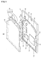
- Fig. 1 is an assembly diagram of a printed circuit board 10 on which an antenna apparatus in accordance with a first embodiment has been mounted.
- Fig. 2 is a top view of the printed circuit board 10 in accordance with the first embodiment.
- Fig. 3 is a front view of the printed circuit board 10 in accordance with the first embodiment.
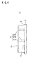
- Fig. 4 is a side view of the printed circuit board 10 in accordance with the first embodiment.
- a printed wiring board 11 has circuit components 14 or the like mounted thereon, an electrode pattern for wiring being formed on a surface of the printed wiring board 11 (and inner layers in the case of a multi-layer board).
- Ground (earth) patterns 11A to which a shielding member 13 is soldered are formed on the top surface of the printed wiring board 11.
- the shielding member 13 is soldered when the antenna apparatus is mounted.
- the ground patterns 11A to which the shielding member 13 is soldered are usually formed by removing a solder-proof resist formed on the top surface of the ground pattern of the printed wiring board 11.
- the shielding member 13 is normally soldered to the printed wiring board 11 at a plurality of locations.
- the printed wiring board 11 may be a multi-layer board or a single-layer board.
- An antenna element 12 is provided substantially in parallel with the printed wiring board 11.
- a feeder terminal (feeding point) 12B electrically connected to the printed wiring board 11 supports an antenna element main body 12A.
- the antenna element 12 is integrally formed with the shielding member 13.
- the shielding member 13 and antenna element 12 can be obtained at the same time from a single metal plate by devising the shapes of their bent portions and dimensions.
- An antenna main body supporting portion 12C has the same length as that of the feeder terminal 12B in the direction perpendicular to the printed wiring board 11, and supports the antenna element 12 on the board when mounted on the board.
- the antenna element main body 12A is maintained in parallel with the board and in the same plane as the planar portion of the shielding member 13.
- Shielding member bent portions 13A also have the same length as the feeder terminal 12B and the antenna main body supporting portion 12C in the direction perpendicular to the printed wiring board 11, and secures and supports the planar portion of the shielding member 13 with respect to the board.
- other shielding member bent portions have also the same length in the direction perpendicular to the printed wiring board 11.
- the antenna main body supporting portion 12C In order to avoid influences on the distribution of current passing through the antenna element 12, the antenna main body supporting portion 12C must be formed perpendicularly to the antenna element main body 12A. In this case, it is preferable not to provide a ground pattern or other types of current passage, including an internal layer in the case of a multi-layer board, under the antenna element 12 of the printed wiring board 11.
- the antenna element soldering pattern 11C is a pattern for fixing by soldering the distal end portion of the antenna main body supporting portion 12C onto the printed wiring board 11, and is not electrically connected to another wiring.
- the feeder terminal 12B vertically formed on the antenna element main body 12A in the same manner as the antenna main body supporting portion 12C is soldered to a soldering pattern 11B on the printed wiring board 11.
- the soldering pattern 11B secures the feeder terminal 12B onto the printed wiring board 11 by soldering, one end thereof being electrically connected to a signal feeding point of a circuit formed on the printed wiring board 11. This allows transmission signals and reception signals of a radio circuit, not shown, to be transferred between the antenna and the radio circuit.
- the antenna element 12 is preferably made of a material, such as copper, which has high electrical conductivity. Alternatively, however, if the material of the antenna element itself does not have such a high electrical conductivity, a material having a high electrical conductivity may be used for plating on the surface of the material having a lower electrical conductivity.
- the antenna element main body 12A and the feeder terminal 12B cooperatively function as an inverse F antenna.
- the position where the feeder terminal 12B is connected to the antenna element main body 12A is set such that a predetermined value of impedance of the inverse F antenna is obtained.
- the impedance value is set, for example, to 50 ⁇ .
- the shielding member 13 is for electromagnetically shielding the circuit components 14, and it covers these circuit components and the peripheries of wiring patterns (not shown).
- the circuit components 14 typically include semiconductor integrated circuits and chip components mainly of 1608 size (outer dimension: 1.6 mm x 0.8 mm), 1005 size (outer dimension: 1.0 mm x 0.5 mm), and 0603 size (outer dimension: 0.6 mm x 0.3 mm).
- the shielding member 13 is connected, through the shielding member bent portions 13A, to the ground (earth) patterns 11A formed on the printed wiring board 11.
- the area of the ground member of the antenna apparatus is large.
- the ground member is actually provided in the surface area of the printed wiring board 11 as largely as possible.
- the length L along a predetermined directional axis X of the shielding member 13 functioning as the ground member is set substantially to 1/4 ⁇ (1/4 wavelength) in order to reduce the effective area of the ground member while improving the performance of the antenna apparatus at the same time.
- a ground member having a length of substantially 1/4 ⁇ or more may of course be used; however, it is desirable to set the length of the shielding member 13 in the predetermined directional axis X to substantially 1/4 ⁇ from the viewpoint of an installation area.
- a central axis Y of a major portion of the antenna element 12 is disposed so as to extend in the direction substantially orthogonal to the directional axis X.
- the shielding member 13 grounded to electromagnetically shield the circuit components, such as the circuit components 14, and wiring patterns is used as the ground member of the antenna element 12.
- the effective area of the ground member is approximately equal to the area occupied on the printed wiring board 11 of the shielding member 13 shown in Fig. 1.
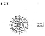
- Fig. 5 is a radiation characteristic diagram of the antenna apparatus according to the first embodiment.
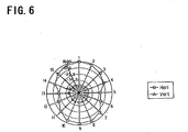
- Fig. 6 is a radiation characteristic diagram of a dipole antenna for a comparison purpose.
- Fig. 7 is a radiation characteristic diagram of an antenna apparatus in which the length in the predetermined directional axis X of the shielding member 13 functioning as a ground member for a comparison purpose is set to a value substantially below 1/4 ⁇ (1/4 wavelength).
- numerals 1 through 16 disposed along the outer peripheral portion denote the directions obtained by equally dividing the full circle 360 degrees by 16, and the actual angular interval between two adjoining numerals is 22.5 degrees.
- Numerical values (dB values) in the figures indicate dipole antenna ratios (dBd).
- Hori denotes a horizontal characteristic
- Vert denotes a vertical characteristic.
- the radiation characteristic exhibits deterioration equal to or within a few dB, as compared with those of the dipole antenna shown in Fig. 6, indicating that the antenna apparatus according to the first embodiment has permitted extremely outstanding radiation characteristics to be achieved.
- the performance of the antenna apparatus deteriorates when the length of the shielding member 13 functioning as the ground member along the predetermined directional axis X is set to a value substantially below 1/4 ⁇ .
- the radiation characteristic deteriorates 10 dB or more, as compared with that of the dipole antenna shown in Fig. 5, indicating that the performance of the antenna apparatus has deteriorated.
- the antenna element and the shielding member have been formed as one piece in the above first embodiment, while the antenna element and the shielding member are separate parts in a second embodiment.
- Fig. 8 is an assembly diagram of a printed circuit board on which an antenna apparatus in accordance with the second embodiment has been mounted.
- Fig. 9 is a top view of the printed circuit board in accordance with the second embodiment.
- Fig. 10 is a front view of the printed circuit board in accordance with the second embodiment.
- primary components disposed on the top surface of a printed wiring board 21 constituting a printed circuit board 20 are an antenna element 22, a shielding member 23 and circuit components 24.
- the printed wiring board 21 may be formed of a single-layer substrate or a multi-layer substrate, as in the case of the first embodiment.
- the antenna element 22 is provided substantially in parallel with the printed wiring board 21 in a three-dimensional fashion.
- a feeder terminal (feeding point) 22B is connected by soldering to the printed wiring board 21 on a soldering pattern 21 B, and an antenna main body supporting portion 22C is soldered to a soldering pattern 21 C.
- the soldering pattern 21 C is a pattern for securing by soldering the distal end portion of the antenna main body supporting portion 22C onto the board, and it is not electrically connected with other wiring.
- an antenna element main body 22A is supported by the feeder terminal 22B and the antenna main body supporting portion 22C.
- the antenna can be positionally secured by providing a plurality of the antenna main body supporting portions 22C on both sides of the element, as shown in the figures.
- One end point of the antenna element 22 is electrically and mechanically connected to the shielding member 23 by soldering, brazing or the like.
- the antenna element 22 is preferably formed of a material, such as copper, that has high electrical conductivity. Alternatively, however, it may have a surface plating with a material having high electrical conductivity.
- the antenna element main body 22A, the feeder terminals 22B and the antenna main body supporting portions 22C cooperatively function as an inverse F antenna.
- the position where the feeder terminal 22B is connected to the antenna element main body 22A is set such that a predetermined value of impedance (e.g., 50 ⁇ ) at 1/4 ⁇ length of the inverse F antenna is obtained.
- the shielding member 23 is for electromagnetically shielding the circuit components 24, and it covers these circuit components and the peripheries of wiring patterns.
- the shielding member 23 is further connected, through shielding member bent portions 23A, to ground (earth) patterns 21A formed on the printed wiring board 21 in the same manner as in the first embodiment described above.
- the length L of the shielding member 23 functioning as the ground member along a predetermined directional axis X is set substantially to 1/4 ⁇ in order to reduce the effective area of the ground member while improving the performance of the antenna apparatus at the same time.
- a ground member having a length of substantially 1/4 ⁇ or more may of course be used; however, it is desirable to set the length of the shielding member 23 in the predetermined directional axis X to substantially 1/4 ⁇ from the viewpoint of an installation area.
- a central axis Y of a major portion of the antenna element 22 is disposed so as to extend in the direction substantially orthogonal to the directional axis X.
- the second embodiment also allows the area of a printed circuit board to be reduced while improving the characteristics of the antenna apparatus at the same time.
- the shielding member 23 grounded to electromagnetically shield the circuit components, such as the circuit components 24, and wiring patterns is used as the ground member of the antenna element 22.
- the shielding member 23 grounded to electromagnetically shield the circuit components, such as the circuit components 24, and wiring patterns is used as the ground member of the antenna element 22.
- the antenna element 22 and the shielding member 23 are formed as discrete components. This requires an additional step for combining the antenna element 22 and the shielding member 23, while the two components can be separately machined, permitting easier machining. In addition, the arrangement permits easier adaptation to a variety of product types.
- the antenna element has been separate from the printed wiring board.
- the antenna element is provided in the form of a printed antenna (wiring pattern) on the printed wiring board.
- Fig. 11 is an assembly diagram of a printed circuit board on which an antenna apparatus in accordance with the third embodiment has been mounted.
- Fig. 12 is a top view of the printed circuit board in accordance with the third embodiment.
- Fig. 13 is a front view of the printed circuit board in accordance with the third embodiment.
- primary components disposed on the top surface of a printed wiring board 31 constituting a printed circuit board 30 are an antenna element main body 32A formed as a wiring pattern, a shielding member 33 and circuit components, such as circuit components 34, and wiring pattern (not shown).
- the printed wiring board 31 may be formed of a single-layer substrate or a multi-layer substrate, as in the case of the foregoing embodiments.
- the antenna element main body 32A is provided in the form of printed wiring on the printed wiring board 31.
- a feeder terminal (feeding point) 32B is electrically connected to power supply wiring on the printed wiring board 31, and one end of the antenna element main body 32A is connected to a ground pattern 31A formed on the printed wiring board 31.
- the patterns may be continuously formed to be the same ground pattern.
- the portion of the ground pattern 31A formed on the printed wiring board 31 that faces the antenna element main body 32A is formed with a predetermined interval substantially in parallel with the antenna element main body 32A.
- the portion of the antenna element main body 32A that is connected to the ground pattern 31A is connected perpendicularly to the ground pattern.
- the antenna element main body 32A and the feeder terminals 32B cooperatively function as an inverse F antenna.
- the position where the feeder terminal 32B is connected to an antenna element 32 is set such that a predetermined value of impedance (e.g., 50 ⁇ ) of the inverse F antenna is obtained.
- a shielding member 33 is for electromagnetically shielding circuit components, such as the circuit components 34, and wiring patterns and it covers these circuit components and the peripheries of the wiring patterns (not shown).
- the shielding member 33 is connected, through shielding member bent portions 33A, to ground (earth) patterns 31A formed on the printed wiring board 31 in the same manner as in the first embodiment described above.
- the length L along a predetermined directional axis X of the shielding member 33 functioning as the ground member is set substantially to 1/4 ⁇ in order to reduce the effective area of the ground member while improving the performance of the antenna apparatus at the same time.
- a ground member having a length of substantially 1/4 ⁇ or more may of course be used; however, it is desirable to set the length of the shielding member 33 in the predetermined directional axis X to substantially 1/4 ⁇ from the viewpoint of an installation area.
- a central axis Y of a major portion of the antenna element main body 32A is disposed so as to extend in the direction substantially orthogonal to the directional axis X.
- the shielding member 33 grounded to electromagnetically shield the circuit components, such as the circuit components 34, and wiring patterns is used as the ground member of the antenna element 32.
- the shielding member 33 grounded to electromagnetically shield the circuit components, such as the circuit components 34, and wiring patterns is used as the ground member of the antenna element 32.
- the antenna element 32 can be provided as the printed wiring when fabricating the printed wiring board, the manufacturing process can be simplified.
- the antenna element has been formed as a printed antenna (wiring pattern) on the printed wiring board.
- a ground member is formed as a ground pattern on a printed wiring board.
- Fig. 14 is a top view of a printed circuit board on which an antenna apparatus in accordance with the fourth embodiment has been mounted.
- Fig. 15 is a front view of the printed circuit board shown in Fig. 14.
- primary components disposed on the top surface of a printed wiring board 41 constituting a printed circuit board 40 are an antenna element 42, a ground pattern 43 formed as a wiring pattern, and circuit components 44.
- the printed wiring board 41 may be formed of a single-layer substrate or a multi-layer substrate, as in the case of the foregoing embodiments.
- the ground pattern 43 may be formed on an inner layer, as necessary.
- An antenna element main body 42A is provided in the form of a printed wiring on the printed wiring board 41.
- a feeder terminal (feeding point) 42B is electrically connected to power supply wiring, not shown, on the printed wiring board 41, while a grounding terminal (grounding point) 42C is electrically connected to the ground pattern 43.
- the performance of an antenna element main body 42A can be improved by plating the surface of the printed wiring with a material having high electrical conductivity.
- the antenna element main body 42A, the feeder terminal 42B and the grounding terminal 42C cooperatively function as an inverse F antenna.
- the position where the feeder terminal 42B is connected to the antenna element main body 42A is set such that a predetermined value of impedance (e.g., 50 ⁇ ) of the inverse F antenna is obtained.
- the ground pattern 43 is appropriately disposed around the circuit components 44.
- the ground pattern is continuously provided as much as possible along a predetermined directional X axis.
- use of a multi-layer substrate permits easier formation of the ground pattern.
- the length L along a predetermined directional axis X of the ground pattern 43 functioning as the ground member is set substantially to 1/4 ⁇ in order to reduce the effective area of the ground member while improving the performance of the antenna apparatus at the same time.
- a ground member having a length of substantially 1/4 ⁇ or more may of course be used; however, it is desirable to set the length of the ground pattern 43 in the predetermined directional axis X to substantially 1/4 ⁇ from the viewpoint of an installation area.
- a central axis Y of a major portion of the antenna element 42 is disposed so as to extend in the direction substantially orthogonal to the directional axis X.
- the manufacturing process can be simplified.
- the shielding member has covered the circuit components over the entire printed wiring board except for the portion where the antenna element is disposed. If, however, there is an allowance on a printed wiring board, it is possible to form the ground pattern electrically connected to the shielding member on the printed wiring board so as to secure the ground area by the shielding member and the ground pattern.
- the antenna element has a bent configuration to fit along the shielding member.
- the antenna element may alternatively have a curved configuration or other configurations as long as it follows the configuration of the shielding member, i.e., it has a configuration parallel with the end portion of the shielding member.
- the microscopic current direction of the current passing through the antenna element is regarded as a vector, and the positions of the components around an antenna element pattern, a wiring pattern or a pad are set so that the foregoing vector is not parallel with the vector (microscopic current direction) of the current passing through the components, the wiring pattern or the pad as much as possible.
- a printed wiring board provides the same advantages if it is provided with a ground member wherein when the wavelength of an electromagnetic wave used for communication is ⁇ , the length along a predetermined directional axis is set substantially to 1/4 ⁇ (or more) and an antenna element disposed to extend in a direction substantially orthogonal to the directional axis and grounded to the ground member, the ground member and the antenna element being formed as printed wiring.
- the antenna element is preferably formed so as to provide a length of 1/4 wavelength at a desired frequency.
- Fig. 16 is an explanatory diagram of a communication adapter module 70 for connection to a portable telephone terminal.
- primary components disposed on the top surface of a printed wiring board 51 constituting a printed circuit board 50 are an antenna element 52 disposed as a wiring pattern, a shielding member 53 and circuit components, such as circuit components 54, and wiring pattern (not shown).
- the printed wiring board 51 may be formed of a single-layer substrate or a multi-layer substrate, as in the case of the foregoing embodiments.
- An antenna element main body 52A is provided in the form of the printed wiring on the printed wiring board 51.
- a feeder terminal (feeding point) 52B is electrically connected to power supply wiring on the printed wiring board 51.
- One end of the antenna element main body 52A is connected to a ground pattern 51A formed on the printed wiring board 51. In this case, the patterns may be formed to be continuous into the same ground pattern.
- the portion of the ground pattern 51A formed on the printed wiring board 51 that faces the antenna element main body 52A is formed with a predetermined interval substantially in parallel with the antenna element main body 52A.
- the portion of the antenna element main body 52A that is connected to the ground pattern 51A is connected perpendicularly to the ground pattern 51A.
- the antenna element main body 52A and the feeder terminals 52B cooperatively function as an inverse F antenna.
- the position where the feeder terminal 52B is connected to the antenna element main body 52A is set such that a predetermined value of impedance (e.g., 50 ⁇ ) of the inverse F antenna is obtained.
- the shielding member 53 is for electromagnetically shielding circuit components, such as the circuit components 54, and wiring patterns (not shown) and it covers these circuit components and the peripheries of the wiring patterns.
- the shielding member 53 is connected, through shielding member bent portions 53A, to ground (earth) patterns 51A formed on the printed wiring board 51 in the same manner as in the third embodiment described above.
- One end of the printed wiring board 51 is provided with a connector connecting terminal block 55.
- the connector connecting terminal block 55 is provided on one side substantially parallel with the direction (direction B: the direction in which the antenna element 52 on the printed wiring board 51 and the shielding member 53 are connected) substantially orthogonal to the direction (direction A in the drawing) in which the antenna element main body 52A extends.
- a plurality of connector connecting terminals (electrode pattern) 56 are formed on the connector connecting terminal block 55.
- Connecting terminals (not shown) of a connector 60 are attached to the connector connecting terminals 56.
- Connecting terminals are, for example, ground terminals, power source terminals and a plurality of signal line terminals for connecting portable telephone terminals and communication adapters.
- the connector connecting terminal block 55 provided on one side substantially in parallel with direction B maintains the relationship between the ground member length (equivalent to 1/4 wavelength) of an antenna and the antenna element when the apparatus is connected to a portable telephone terminal, thus preventing antenna gain from being degraded.
- FIG. 17 is an external perspective view of a communication adapter module 70 connected by inserting a connector 60 shown in Fig. 16 into the printed circuit board 50.
- a battery, a case 61, etc. are added and installed to the communication adapter module 70 to complete a communication adapter 80 (finished product), as shown in Fig. 18.
- Fig. 19 is a layout explanatory diagram showing the communication adapter 80 used by being connected to a portable telephone terminal 81.
- the bottom portion of the portable telephone terminal 81 (connector terminals (not shown) for external connection is provided on the right-hand side in the drawing) and a connector terminal 82 (refer to Fig. 18) of the communication adapter 80 are inserted and fitted to each other to establish electrical connection.
- the connection to the portable telephone terminal 81 will not deteriorate the antenna characteristics of the communication adapter 80.
- Fig. 20 is an antenna directivity characteristic diagram of the communication adapter 80 alone without the portable telephone terminal 81 connected thereto.
- Fig. 21 is a radiation directivity characteristic diagram of an antenna apparatus obtained by connecting the communication adapter 80 and the portable telephone terminal 81.
- the numerals 1 through 16 disposed along the outer peripheral portion in the drawings denote the directions obtained by equally dividing the full circle 360 degrees by 16, the actual angular interval between two adjacent numerals is 22.5 degrees.
- Numerical values (dB values) in the graphs indicate dipole antenna ratios (dBd).
- the antenna directivity characteristic of the communication adapter 80 alone is good, as shown in Fig. 20.
- the antenna directivity characteristic observed when the communication adapter 80 and the portable telephone terminal 81 are connected does not exhibit characteristic deterioration; rather, it can be seen that the gain improves, as shown in Fig. 21.
- the communication adapter 80 described above is connected to the portable telephone terminal 81 and used in combination with another radio terminal apparatus by a predetermined radio communication technology. More specifically, the communication adapter 80 is used in combination with a head set, a hands-free set or the like serving as another radio terminal apparatus by using the Bluetooth, weak radio, etc. as a radio communication technology, and used for a hands-free unit of a portable telephone in a car.
- the communication adapter 80 can be also used as a short-distance radio communication system indoors, outdoors or the like, thus permitting information communication with another radio communication equipment.
- the antenna directivity characteristic exhibited when used in combination with a portable telephone terminal is more important than the characteristics of the antenna alone.
- the construction of the present embodiment is extremely effective for such an application.
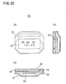
- Fig. 22 shows the configuration of a wristwatch type (watch type) wireless apparatus 90 using the printed circuit board described in the foregoing first through fourth embodiments and the modification examples.
- Fig. 22 (a) is a top view
- Fig. 22 (b) is a front sectional view
- Fig. 22 (c) is a side sectional view.
- an antenna apparatus 94 is constructed such that a shielding member 95 is located on the bottom side (wrist side). This construction is convenient for providing a conduction rubber component 93 for transmitting display drive signals to a display 92 at the opposite side from a shielding member 95 of the antenna apparatus 94.
- Two (for two systems) conduction rubber components 93 are usually provided on top and bottom (or right and left) of the display 92, as shown in Fig. 22 (c).
- the wristwatch type wireless apparatus 90 all the parts constituting the wristwatch type wireless apparatus 90 are accommodated in a watchcase 91.
- the shielding member 95 is located at the bottom, making it suited for disposing a battery 96, which is a metal unit, in a layered fashion.
- the battery 96 disposed as mentioned above is preferably set such that its orthogonal projection stays within a region wherein a ground pattern of the antenna apparatus 94 is disposed when the printed wiring board constituting the antenna apparatus 94 is regarded as a plane.
- the anode of the battery 96 can be connected to a circuit through the shielding member 95, permitting a smaller size to be achieved.
- Fig. 23 and Fig. 24 are explanatory diagrams of configuration examples of PDAs (Personal Digital Assistant: portable information processor) 100 and 110 using a printed circuit board of those described in the foregoing first through fourth embodiments and modification examples.
- PDAs Personal Digital Assistant: portable information processor
- Fig. 23 is an explanatory diagram of a configuration example applied when an antenna apparatus 101 according to a sixth embodiment is connected to a circuit board 102 of the PDA 100 by a connector or the like.
- Fig. 23 (a) is a top plan view and Fig. 23 (b) is a sectional view.
- the antenna apparatus 101 and the circuit board 102 are layered in the direction of thickness and connected by inter-board connectors 103 and 104.
- the antenna apparatus 101 and the circuit board 102 are preferably apart from each other by a predetermined distance. For example, a few centimeters or more is provided therebetween.
- the thicknesses of the inter-board connectors 103 and 104 are appropriately set so as to set the interval between the circuit board 102 and the antenna apparatus 101 to such predetermined distance.
- the pattern on the circuit board 102 opposing the antenna element of the antenna apparatus 101 is not a large pattern like a ground pattern or the like.
- the portion of the antenna apparatus 101 excluding the antenna element is shielded by a shielding member 105.
- a display 106 is provided on the front surface of the PDA 100.
- Fig. 24 illustrates a layout example for building an antenna apparatus 111 in accordance with the sixth embodiment into a circuit board 112 of the PDA 110.
- Fig. 24 (a) is a top plan view of the PDA 110 seen through, and
- Fig. 24 (b) is a sectional view.
- a region in which the antenna apparatus 111 is to be formed is provided on the circuit board 112, and only the antenna apparatus 111 is formed in that region.
- the wiring pattern of the PDA circuit 113 itself is formed in the remaining portion on the circuit board 112. Necessary signal lines are connected between the PDA circuit 113 and the antenna apparatus 111 only through a pattern connection portion 114.
- the portion of the antenna apparatus 111 excluding the antenna element is shielded by the shielding member 115.
- the front surface of the PDA 110 is provided with a display 116.
- the length L, in the predetermined directional axis X, of the shielding member 13 functioning as the ground member is set substantially to 1/4 ⁇ .
- the shielding member is used as the ground member, a sufficient ground area can be securely obtained even if the area of a printed wiring board is too small to secure an ample ground area.
- the apparatus can be made smaller with a higher mounting density, while restraining deterioration in antenna sensitivity.
- an antenna apparatus it is possible to reduce the size of an antenna apparatus and consequently reduce the size of a printed wiring board or a printed circuit board made integral with an antenna apparatus, while improving the characteristics of the antenna apparatus at the same time. Furthermore, a communication adapter and portable electronic equipment incorporating an antenna apparatus can be made smaller.
- the shielding member is used as the ground member of an antenna, even if the area of a printed wiring board is too small to secure an ample ground area, the mounting density can be increased while restraining the deterioration in antenna sensitivity, allowing compact radio communication equipment to be made.
- the present invention is especially suited to applications wherein reduced sizes are desired, as in the case of wristwatch type radio communication equipment (wristwatch type portable electronic equipment).
Applications Claiming Priority (4)
| Application Number | Priority Date | Filing Date | Title |
|---|---|---|---|
| JP2002266323 | 2002-09-12 | ||
| JP2002266323 | 2002-09-12 | ||
| JP2003157951 | 2003-06-03 | ||
| JP2003157951A JP2004159288A (ja) | 2002-09-12 | 2003-06-03 | アンテナ装置、プリント配線板、プリント基板、通信アダプタおよび携帯型電子機器 |
Publications (1)
| Publication Number | Publication Date |
|---|---|
| EP1398847A1 true EP1398847A1 (de) | 2004-03-17 |
Family
ID=31890569
Family Applications (1)
| Application Number | Title | Priority Date | Filing Date |
|---|---|---|---|
| EP20030020422 Ceased EP1398847A1 (de) | 2002-09-12 | 2003-09-11 | Antennenanordnung, Leiterplatte, Kommunikations-Adapter und tragbares elektronisches Gerät |
Country Status (4)
| Country | Link |
|---|---|
| US (1) | US6946996B2 (de) |
| EP (1) | EP1398847A1 (de) |
| JP (1) | JP2004159288A (de) |
| CN (1) | CN1271746C (de) |
Cited By (11)
| Publication number | Priority date | Publication date | Assignee | Title |
|---|---|---|---|---|
| WO2006102364A1 (en) * | 2005-03-23 | 2006-09-28 | Kyocera Wireless Corp. | Patch antenna with electromagnetic shield counterpoise |
| WO2009125214A1 (en) * | 2008-04-08 | 2009-10-15 | Antenova Limited | A novel planar radio-antenna module |
| EP2112767A1 (de) * | 2006-09-13 | 2009-10-28 | Toa Corporation | Drahtlose mikrofonanordnung |
| WO2011066303A1 (en) * | 2009-11-24 | 2011-06-03 | Digi International Inc. | Wideband antenna for printed circuit boards |
| US8138979B2 (en) | 2006-02-24 | 2012-03-20 | Kyocera Corporation | Portable wireless apparatus |
| CN102569989A (zh) * | 2010-12-29 | 2012-07-11 | 纬创资通股份有限公司 | 天线模块 |
| EP2902798A1 (de) * | 2014-02-04 | 2015-08-05 | Furuno Electric Co., Ltd. | Radarantenne |
| DE102006023206B4 (de) * | 2005-05-18 | 2018-01-04 | Denso Corporation | In einem Fahrzeug anordenbares Antennensystem |
| GB2567812A (en) * | 2017-10-19 | 2019-05-01 | Raspberry Pi Trading Ltd | Radio module |
| US11291145B2 (en) | 2019-05-29 | 2022-03-29 | Hewlett Packard Enterprise Development Lp | Integrated antenna device |
| EP3799544B1 (de) * | 2019-09-30 | 2023-07-19 | Hager Controls | Steuergeräte für haustechnikanlage |
Families Citing this family (42)
| Publication number | Priority date | Publication date | Assignee | Title |
|---|---|---|---|---|
| US9066695B2 (en) | 1998-04-30 | 2015-06-30 | Abbott Diabetes Care Inc. | Analyte monitoring device and methods of use |
| US8465425B2 (en) | 1998-04-30 | 2013-06-18 | Abbott Diabetes Care Inc. | Analyte monitoring device and methods of use |
| US8480580B2 (en) | 1998-04-30 | 2013-07-09 | Abbott Diabetes Care Inc. | Analyte monitoring device and methods of use |
| US8346337B2 (en) | 1998-04-30 | 2013-01-01 | Abbott Diabetes Care Inc. | Analyte monitoring device and methods of use |
| US6949816B2 (en) | 2003-04-21 | 2005-09-27 | Motorola, Inc. | Semiconductor component having first surface area for electrically coupling to a semiconductor chip and second surface area for electrically coupling to a substrate, and method of manufacturing same |
| US6175752B1 (en) | 1998-04-30 | 2001-01-16 | Therasense, Inc. | Analyte monitoring device and methods of use |
| US8974386B2 (en) | 1998-04-30 | 2015-03-10 | Abbott Diabetes Care Inc. | Analyte monitoring device and methods of use |
| US8688188B2 (en) | 1998-04-30 | 2014-04-01 | Abbott Diabetes Care Inc. | Analyte monitoring device and methods of use |
| US6560471B1 (en) | 2001-01-02 | 2003-05-06 | Therasense, Inc. | Analyte monitoring device and methods of use |
| EP1397068A2 (de) | 2001-04-02 | 2004-03-17 | Therasense, Inc. | Gerät und verfahren zur blutzuckerverfolgung |
| TW575258U (en) * | 2003-05-23 | 2004-02-01 | Quanta Comp Inc | Wireless communication device |
| JP4013839B2 (ja) * | 2003-06-17 | 2007-11-28 | ミツミ電機株式会社 | アンテナ装置 |
| JP2005176307A (ja) * | 2003-11-19 | 2005-06-30 | Matsushita Electric Ind Co Ltd | アンテナ素子及びそれを用いたループアンテナ並びに無線通信媒体処理装置 |
| TWI273737B (en) * | 2004-07-23 | 2007-02-11 | Asustek Comp Inc | Antenna device |
| JP2006344716A (ja) * | 2005-06-08 | 2006-12-21 | Mitsumi Electric Co Ltd | アンテナ装置およびそれに用いられるシールドカバー |
| CN101034907A (zh) * | 2006-03-07 | 2007-09-12 | 鸿富锦精密工业(深圳)有限公司 | 电子设备及其信号收发装置 |
| US20070216580A1 (en) * | 2006-03-15 | 2007-09-20 | Chant Sincere Co., Ltd. | Electro-stimulating massage confiner |
| US7920907B2 (en) | 2006-06-07 | 2011-04-05 | Abbott Diabetes Care Inc. | Analyte monitoring system and method |
| KR20100049811A (ko) * | 2008-11-04 | 2010-05-13 | 주식회사 모비텍 | 커플링을 이용한 인체 영향 저감용 내장형 안테나 |
| CN101877431A (zh) * | 2009-04-30 | 2010-11-03 | 深圳富泰宏精密工业有限公司 | 平面倒f天线及具有该平面倒f天线的便携式电子装置 |
| US8698675B2 (en) | 2009-05-12 | 2014-04-15 | Ruckus Wireless, Inc. | Mountable antenna elements for dual band antenna |
| CN201438500U (zh) * | 2009-06-05 | 2010-04-14 | 鸿富锦精密工业(深圳)有限公司 | 多输入输出电子设备 |
| JP5333366B2 (ja) * | 2010-07-07 | 2013-11-06 | オムロン株式会社 | ネットワーク機器および通信モジュール |
| US8723733B2 (en) * | 2010-09-29 | 2014-05-13 | Qualcomm Incorporated | Multiband antenna for a mobile device |
| CN102509883A (zh) * | 2011-12-08 | 2012-06-20 | 鸿富锦精密工业(深圳)有限公司 | 可抑制天线间相互干扰的天线结构 |
| EP2880709A1 (de) | 2012-07-30 | 2015-06-10 | UTC Fire & Security Americas Corporation, Inc. | Ism-band-antennenstruktur für ein sicherheitssystem |
| US9570799B2 (en) | 2012-09-07 | 2017-02-14 | Ruckus Wireless, Inc. | Multiband monopole antenna apparatus with ground plane aperture |
| CN105051975B (zh) | 2013-03-15 | 2019-04-19 | 艾锐势有限责任公司 | 用于双频带定向天线的低频带反射器 |
| EP2854214A1 (de) | 2013-09-27 | 2015-04-01 | Thomson Licensing | Antennenanordnung für eine elektronische Vorrichtung |
| TWI528632B (zh) * | 2013-11-28 | 2016-04-01 | 矽品精密工業股份有限公司 | 電子封裝件及其製法 |
| TWI546928B (zh) * | 2014-03-17 | 2016-08-21 | 矽品精密工業股份有限公司 | 電子封裝件及其製法 |
| CN103838137A (zh) * | 2014-03-21 | 2014-06-04 | 成都天奥电子股份有限公司 | 一种集成小天线的卫星授时手表 |
| CN104064857A (zh) * | 2014-07-04 | 2014-09-24 | 信维创科通信技术(北京)有限公司 | 适用于穿戴式设备的无线电通讯天线及穿戴式设备 |
| KR20160066358A (ko) * | 2014-12-02 | 2016-06-10 | 삼성전기주식회사 | 무선 통신 모듈 |
| JP6593202B2 (ja) * | 2016-01-29 | 2019-10-23 | セイコーエプソン株式会社 | 電子部品および腕時計 |
| CN106061110A (zh) * | 2016-06-28 | 2016-10-26 | 广东欧珀移动通信有限公司 | Pcb板及具有其的移动终端 |
| US10191152B2 (en) | 2016-07-29 | 2019-01-29 | Honeywell International Inc. | Low-cost lightweight integrated antenna for airborne weather radar |
| US10581141B2 (en) | 2016-10-21 | 2020-03-03 | DISH Technologies L.L.C. | RF antenna arrangement configured to be a part of a lid to an apparatus |
| US10320055B2 (en) | 2017-04-28 | 2019-06-11 | DISH Technologies L.L.C. | Radio frequency antenna for short range communications |
| CN108170023A (zh) * | 2018-02-28 | 2018-06-15 | 深圳市沃特沃德股份有限公司 | 可穿戴设备 |
| KR20210101091A (ko) * | 2020-02-07 | 2021-08-18 | 삼성전자주식회사 | mmWave 안테나 모듈을 포함하는 전자 장치 |
| CN113314826B (zh) * | 2021-06-07 | 2022-03-04 | 深圳微蓝电子有限公司 | 天线结构及无线传输装置 |
Citations (4)
| Publication number | Priority date | Publication date | Assignee | Title |
|---|---|---|---|---|
| EP0757405A1 (de) * | 1995-08-03 | 1997-02-05 | Nokia Mobile Phones Ltd. | Antenne |
| US6147652A (en) * | 1997-09-19 | 2000-11-14 | Kabushiki Kaisha Toshiba | Antenna apparatus |
| US6392603B1 (en) * | 1999-10-29 | 2002-05-21 | Telefonaktiebolaget Lm Ericsson (Publ) | Module antenna device |
| US20020126047A1 (en) * | 2001-03-07 | 2002-09-12 | Laureanti Steven J. | Planar inverted-F antenna |
Family Cites Families (11)
| Publication number | Priority date | Publication date | Assignee | Title |
|---|---|---|---|---|
| JPH01245721A (ja) * | 1988-03-28 | 1989-09-29 | Matsushita Electric Works Ltd | 無線装置 |
| JPH03175826A (ja) | 1989-12-05 | 1991-07-30 | Matsushita Electric Ind Co Ltd | 携帯形電話機 |
| NL9302192A (nl) * | 1993-07-09 | 1995-02-01 | Ericsson Business Mobile Netwo | Draadloze telefoon. |
| US6204825B1 (en) * | 1997-04-10 | 2001-03-20 | Intermec Ip Corp. | Hybrid printed circuit board shield and antenna |
| JPH118508A (ja) | 1997-06-19 | 1999-01-12 | Fujitsu Ltd | 移動端末内蔵アンテナ |
| US6539207B1 (en) * | 2000-06-27 | 2003-03-25 | Symbol Technologies, Inc. | Component for a wireless communications equipment card |
| US6380903B1 (en) * | 2001-02-16 | 2002-04-30 | Telefonaktiebolaget L.M. Ericsson | Antenna systems including internal planar inverted-F antennas coupled with retractable antennas and wireless communicators incorporating same |
| US6466170B2 (en) * | 2001-03-28 | 2002-10-15 | Motorola, Inc. | Internal multi-band antennas for mobile communications |
| JP3763764B2 (ja) * | 2001-09-18 | 2006-04-05 | シャープ株式会社 | 板状逆fアンテナ及び無線通信装置 |
| US6819287B2 (en) * | 2002-03-15 | 2004-11-16 | Centurion Wireless Technologies, Inc. | Planar inverted-F antenna including a matching network having transmission line stubs and capacitor/inductor tank circuits |
| TW555177U (en) * | 2002-11-29 | 2003-09-21 | Hon Hai Prec Ind Co Ltd | Multi-band antenna |
-
2003
- 2003-06-03 JP JP2003157951A patent/JP2004159288A/ja active Pending
- 2003-09-10 CN CNB031568580A patent/CN1271746C/zh not_active Expired - Fee Related
- 2003-09-11 EP EP20030020422 patent/EP1398847A1/de not_active Ceased
- 2003-09-12 US US10/661,353 patent/US6946996B2/en not_active Expired - Lifetime
Patent Citations (4)
| Publication number | Priority date | Publication date | Assignee | Title |
|---|---|---|---|---|
| EP0757405A1 (de) * | 1995-08-03 | 1997-02-05 | Nokia Mobile Phones Ltd. | Antenne |
| US6147652A (en) * | 1997-09-19 | 2000-11-14 | Kabushiki Kaisha Toshiba | Antenna apparatus |
| US6392603B1 (en) * | 1999-10-29 | 2002-05-21 | Telefonaktiebolaget Lm Ericsson (Publ) | Module antenna device |
| US20020126047A1 (en) * | 2001-03-07 | 2002-09-12 | Laureanti Steven J. | Planar inverted-F antenna |
Cited By (18)
| Publication number | Priority date | Publication date | Assignee | Title |
|---|---|---|---|---|
| AU2006227102B2 (en) * | 2005-03-23 | 2009-11-05 | Kyocera Corporation | Patch antenna with electromagnetic shield counterpoise |
| US7629928B2 (en) | 2005-03-23 | 2009-12-08 | Kyocera Wireless Corp. | Patch antenna with electromagnetic shield counterpoise |
| WO2006102364A1 (en) * | 2005-03-23 | 2006-09-28 | Kyocera Wireless Corp. | Patch antenna with electromagnetic shield counterpoise |
| DE102006023206B4 (de) * | 2005-05-18 | 2018-01-04 | Denso Corporation | In einem Fahrzeug anordenbares Antennensystem |
| US8138979B2 (en) | 2006-02-24 | 2012-03-20 | Kyocera Corporation | Portable wireless apparatus |
| EP2112767A1 (de) * | 2006-09-13 | 2009-10-28 | Toa Corporation | Drahtlose mikrofonanordnung |
| EP2112767A4 (de) * | 2006-09-13 | 2010-02-03 | Toa Corp | Drahtlose mikrofonanordnung |
| US9413071B2 (en) | 2008-04-08 | 2016-08-09 | Microsoft Technology Licensing, Llc | Planar radio-antenna module |
| WO2009125214A1 (en) * | 2008-04-08 | 2009-10-15 | Antenova Limited | A novel planar radio-antenna module |
| US8599093B2 (en) | 2009-11-24 | 2013-12-03 | Digi International Inc. | Wideband antenna for printed circuit boards |
| WO2011066303A1 (en) * | 2009-11-24 | 2011-06-03 | Digi International Inc. | Wideband antenna for printed circuit boards |
| CN102569989A (zh) * | 2010-12-29 | 2012-07-11 | 纬创资通股份有限公司 | 天线模块 |
| CN102569989B (zh) * | 2010-12-29 | 2015-03-25 | 纬创资通股份有限公司 | 天线模块 |
| EP2902798A1 (de) * | 2014-02-04 | 2015-08-05 | Furuno Electric Co., Ltd. | Radarantenne |
| US9910147B2 (en) | 2014-02-04 | 2018-03-06 | Furuno Electric Co., Ltd. | Radar antenna |
| GB2567812A (en) * | 2017-10-19 | 2019-05-01 | Raspberry Pi Trading Ltd | Radio module |
| US11291145B2 (en) | 2019-05-29 | 2022-03-29 | Hewlett Packard Enterprise Development Lp | Integrated antenna device |
| EP3799544B1 (de) * | 2019-09-30 | 2023-07-19 | Hager Controls | Steuergeräte für haustechnikanlage |
Also Published As
| Publication number | Publication date |
|---|---|
| CN1271746C (zh) | 2006-08-23 |
| US6946996B2 (en) | 2005-09-20 |
| US20040119654A1 (en) | 2004-06-24 |
| CN1494180A (zh) | 2004-05-05 |
| JP2004159288A (ja) | 2004-06-03 |
Similar Documents
| Publication | Publication Date | Title |
|---|---|---|
| US6946996B2 (en) | Antenna apparatus, printed wiring board, printed circuit board, communication adapter and portable electronic equipment | |
| US6958732B2 (en) | Small-sized and high-gained antenna-integrated module | |
| CN111193110B (zh) | 天线装置及电子设备 | |
| US6842093B2 (en) | Radio frequency circuit module on multi-layer substrate | |
| US6031494A (en) | Handy-phone with shielded high and low frequency circuits and planar antenna | |
| EP1418642A2 (de) | Gerät zur drahtlosen Kommunikation | |
| JP5928621B2 (ja) | アンテナ装置および通信端末装置 | |
| EP1032076B1 (de) | Antennenanordnung und Funkgerät mit einer derartigen Antennenanordnung | |
| US10224604B2 (en) | Antenna device and communication terminal device | |
| JP2002353842A (ja) | 携帯端末用無線モジュール | |
| JP3374604B2 (ja) | 無線通信装置 | |
| JP4379004B2 (ja) | 通信アダプタおよび携帯型電子機器 | |
| JP4372325B2 (ja) | アンテナ | |
| JP2002152353A (ja) | 携帯端末機 | |
| JP2830743B2 (ja) | シールドループアンテナ | |
| JP2007329735A (ja) | 無線通信モジュールおよびその製造方法 | |
| WO2016186092A1 (ja) | アンテナ装置および電子機器 | |
| JP7247614B2 (ja) | アンテナ装置、及び、無線通信装置 | |
| CN212968062U (zh) | 一种天线组件、手表及电子设备 | |
| JPH10229304A (ja) | 携帯無線機用アンテナおよびそれを用いた携帯無線機 | |
| JP2005033551A (ja) | 携帯無線通信装置 | |
| JP4421243B2 (ja) | シャーシとプリント基板から成る組合せ構造体 | |
| CN117832843A (en) | Antenna and electronic equipment | |
| JP2019115076A (ja) | アンテナモジュール及び通信装置 | |
| CN117296207A (zh) | 天线 |
Legal Events
| Date | Code | Title | Description |
|---|---|---|---|
| PUAI | Public reference made under article 153(3) epc to a published international application that has entered the european phase |
Free format text: ORIGINAL CODE: 0009012 |
|
| AK | Designated contracting states |
Kind code of ref document: A1 Designated state(s): AT BE BG CH CY CZ DE DK EE ES FI FR GB GR HU IE IT LI LU MC NL PT RO SE SI SK TR |
|
| AX | Request for extension of the european patent |
Extension state: AL LT LV MK |
|
| 17P | Request for examination filed |
Effective date: 20040831 |
|
| AKX | Designation fees paid |
Designated state(s): DE FI FR GB |
|
| 17Q | First examination report despatched |
Effective date: 20050125 |
|
| STAA | Information on the status of an ep patent application or granted ep patent |
Free format text: STATUS: THE APPLICATION HAS BEEN REFUSED |
|
| 18R | Application refused |
Effective date: 20060927 |