EP1398811A2 - Switchable capacitor - Google Patents
Switchable capacitor Download PDFInfo
- Publication number
- EP1398811A2 EP1398811A2 EP20030020159 EP03020159A EP1398811A2 EP 1398811 A2 EP1398811 A2 EP 1398811A2 EP 20030020159 EP20030020159 EP 20030020159 EP 03020159 A EP03020159 A EP 03020159A EP 1398811 A2 EP1398811 A2 EP 1398811A2
- Authority
- EP
- European Patent Office
- Prior art keywords
- armature
- electrode
- overlap
- bottom electrode
- floating electrode
- Prior art date
- Legal status (The legal status is an assumption and is not a legal conclusion. Google has not performed a legal analysis and makes no representation as to the accuracy of the status listed.)
- Granted
Links
Images


Classifications
-
- H—ELECTRICITY
- H01—ELECTRIC ELEMENTS
- H01H—ELECTRIC SWITCHES; RELAYS; SELECTORS; EMERGENCY PROTECTIVE DEVICES
- H01H59/00—Electrostatic relays; Electro-adhesion relays
- H01H59/0009—Electrostatic relays; Electro-adhesion relays making use of micromechanics
-
- B—PERFORMING OPERATIONS; TRANSPORTING
- B81—MICROSTRUCTURAL TECHNOLOGY
- B81B—MICROSTRUCTURAL DEVICES OR SYSTEMS, e.g. MICROMECHANICAL DEVICES
- B81B3/00—Devices comprising flexible or deformable elements, e.g. comprising elastic tongues or membranes
- B81B3/0002—Arrangements for avoiding sticking of the flexible or moving parts
- B81B3/001—Structures having a reduced contact area, e.g. with bumps or with a textured surface
-
- H—ELECTRICITY
- H01—ELECTRIC ELEMENTS
- H01G—CAPACITORS; CAPACITORS, RECTIFIERS, DETECTORS, SWITCHING DEVICES OR LIGHT-SENSITIVE DEVICES, OF THE ELECTROLYTIC TYPE
- H01G5/00—Capacitors in which the capacitance is varied by mechanical means, e.g. by turning a shaft; Processes of their manufacture
- H01G5/16—Capacitors in which the capacitance is varied by mechanical means, e.g. by turning a shaft; Processes of their manufacture using variation of distance between electrodes
- H01G5/18—Capacitors in which the capacitance is varied by mechanical means, e.g. by turning a shaft; Processes of their manufacture using variation of distance between electrodes due to change in inclination, e.g. by flexing, by spiral wrapping
-
- B—PERFORMING OPERATIONS; TRANSPORTING
- B81—MICROSTRUCTURAL TECHNOLOGY
- B81B—MICROSTRUCTURAL DEVICES OR SYSTEMS, e.g. MICROMECHANICAL DEVICES
- B81B2201/00—Specific applications of microelectromechanical systems
- B81B2201/01—Switches
- B81B2201/012—Switches characterised by the shape
- B81B2201/016—Switches characterised by the shape having a bridge fixed on two ends and connected to one or more dimples
-
- B—PERFORMING OPERATIONS; TRANSPORTING
- B81—MICROSTRUCTURAL TECHNOLOGY
- B81C—PROCESSES OR APPARATUS SPECIALLY ADAPTED FOR THE MANUFACTURE OR TREATMENT OF MICROSTRUCTURAL DEVICES OR SYSTEMS
- B81C2201/00—Manufacture or treatment of microstructural devices or systems
- B81C2201/11—Treatments for avoiding stiction of elastic or moving parts of MEMS
- B81C2201/115—Roughening a surface
Definitions
- the present invention relates to electronic devices, especially micro electromechanical (MEMS) devices and method of making the same.
- MEMS micro electromechanical
- the present invention relates to the field of radio frequency MEMS and more particularly the present invention relates to MEMS near-DC to RF capacitive shunt and series switches, e.g. a switchable capacitor.
- RF-MEMS switches offer great potential benefits over GaAs MMICs and PIN (positive intrinsic negative) diode switches for application in wireless communication systems as is described by C. T.-G. Nguyen, et al., in "Micromachined devices for wireless communications", Proc. of the IEEE, vol. 86(8), 1998, pp. 1756-1768, by J. J. Yao, in " RF MEMS from a device perspective ", J. Micromech. Microeng., vol.10(4), December 2000, pp. R9-R38 and by G. M. Rebeiz and J. B. Muldavin, in “ RF MEMS switches and switch circuits ", IEEE Microwave magazine, Dec. 2001, pp. 59-71.
- Prototype RF-MEMS switches display low loss ( ⁇ 0.4 dB), good isolation (>20 dB), extremely low standby power consumption, excellent linearity (IP3>66dBm), compactness and high levels of integration as discussed by J. J. Yao, in " RF MEMS from a device perspective ", J. Micromech. Microeng., vol.10(4), December 2000, pp. R9-R38, by G. M. Rebeiz and J. B. Muldavin, in " RF MEMS switches and switch circuits", IEEE Microwave magazine, Dec. 2001, pp. 59-71, by Z. J. Yao, et al., in “Micromachined low-loss microwave switches ", IEEE J. of MEMS, vol.
- FIG. 1 A typical build-up of a RF-MEMS capacitive switch in a shunt configuration implemented on a CPW (CoPlanar Waveguide) line is shown in Fig. 1 and has been discussed in by Z. J. Yao, et al., in "Micromachined low-loss microwave switches", IEEE J. of MEMS, vol. 8(2), 1999, pp. 129-134, by J. B. Muldavin and G. M. Rebeiz, in "High-isolation CPW MEMS shunt switches-Part 1: Modeling", IEEE Trans. Microwave Theory and Techniques, vol. 48(6), 2000, pp. 1045-1052 and by H. A. C.
- the switch consists of a suspended movable metal bridge, which is mechanically anchored and electrically connected to the ground of the CPW.
- the switch can be modeled as a capacitor between the metal bridge and the signal line.
- the bridge In the RF-ON state the bridge is up, hence the switch capacitance is small, hardly affecting the impedance of the line.
- a DC. bias (superimposed on the RF signal) the bridge is pulled down onto the dielectric, the switch capacitance becomes high and the switch is OFF or in the isolation state.
- An important figure of merit quantifying the RF performance is the down/up capacitance ratio, C down /C up , which is preferably as high as possible.
- a second problem encountered in capacitive switches of the type shown in Fig. 1 is the degradation of the effective down capacitance as a result of surface roughness preventing intimate contact between the beam and the dielectric, which is discussed by J. B. Muldavin and G. M. Rebeiz in "High-isolation CPW MEMS shunt switches-Part 1: Modeling", IEEE Trans. Microwave Theory and Techniques, vol. 48(6), 2000, pp. 1045-1052. Solutions commonly pursued to attain a large down capacitance are aimed at keeping the roughness of the bridge and of the dielectric layer very low, e.g., ⁇ 5 nm, and to keep the surface free from residues. Muldavin et al. and Yao et al.
- a micro electromechanical switch (Fig. 2) comprising a bottom electrode 1, a dielectric layer 2 disposed on the bottom electrode 1, a metal cap (not shown) disposed on the dielectric layer 2 and a bridge 3 disposed proximate to the metal cap such that an electrical potential applied between the bridge 3 and bottom electrode 1 causes the bridge 3 to deform and contact the metal cap.
- the deformed bridge is depicted with reference number 4.
- a problem with this device is that charging of the metal cap will reduce the force exercised on the bridge 3, which might bounce back into the original position, hereby disturbing the normal working of the switch.
- It is an object of the present invention is to provide an electronic device and method of manufacture of the same which a) has an acceptable insertion loss, and/or b) do not require ultra-smooth surfaces and/or c) do not have an unacceptable bounce back.
- the present invention is applicable in the field of switchable capacitors and capacitive switches.
- the present invention provides a micro electromechanical switchable capacitor, a shunt switch or a series switch (corresponding to bridge and cantilever) with relay actuation or actuation in zones attached to a floating electrode area.
- a micro electromechanical switchable capacitor comprising a substrate, a bottom electrode, a dielectric layer deposited on at least part of the bottom electrode, a conductive floating electrode deposited on at least part of the dielectric layer, an armature positioned proximate to the floating electrode so as to form an overlap with the floating electrode, the overlap being defined by projection of the armature onto the floating electrode along a direction substantially perpendicular to the plane of the bottom electrode.
- the switchable capacitor of the present invention comprises a first actuation area, which is defined by a part of an overlap between the armature and the bottom electrode which is not covered by the floating electrode, the overlap between the armature and the bottom electrode being defined by projection of the armature onto the bottom electrode along a direction substantially perpendicular to the bottom electrode.
- the switchable capacitor of the present invention may furthermore comprise at least one actuation electrode and a second actuation area, which second actuation area may be defined by an overlap between the armature and the at least one actuation electrode, the overlap being defined by projection of the armature onto the bottom electrode in a direction substantially perpendicular to the plane of the bottom electrode.
- the overlap between the floating electrode and the armature which overlap is defined by projection of the armature onto the floating electrode in a direction substantially perpendicular to the plane of the bottom electrode, may be made as small as possible in order to decrease the up state capacitance and hence increase the down/up capacitance ratio.
- the capacitor comprises a first and a second side opposite to each other in a plane substantially parallel to the plane of the bottom electrode.
- the armature may be located such that a first part of the floating electrode is positioned at the first side of the armature and a second part of the floating electrode is positioned at the second side of the armature.
- the armature may be a bridge or a cantilever.
- An up state actuation area may be defined by the overlap between the armature and the bottom electrode and/or by the second actuation area.
- a down state actuation area may be defined by the first actuation area and/or by the second actuation area.
- Cup may be defined as the up state capacitance which may be a function of the overlap area between the armature and the bottom electrode. In a further embodiment the up state capacitance may be proportional with the overlap between the armature and the bottom electrode.
- the up state capacitance may be made as low as possible, in order to increase the down/up capacitance ratio, by reducing the overlap between the armature and the bottom electrode.
- C down may be defined as the down state capacitance which may be a function of the overlap area between the floating electrode and the bottom electrode, which overlap may be defined by projection of the floating electrode onto the bottom electrode according to a direction substantially perpendicular to the plane of the bottom electrode.
- the down state capacitance may be proportional with the overlap between the floating electrode and the bottom electrode.
- the floating electrode may consist of two or more unconnected regions.
- each of the unconnected regions may have an overlap with the armature, the overlap being defined by projection of the armature onto the unconnected regions of the floating electrode according to a direction substantially perpendicular to the plane of the bottom electrode.
- At least one superincumbent island of conductive material may be deposited on the floating electrode.
- the at least one superincumbent island functions as a contactor between the armature and the floating electrode.
- the armature comprising an up and down surface positioned opposite of each other in a plane substantially perpendicular to the plane of the bottom electrode, may comprise on its down surface at least one superincumbent island of conductive material.
- the at least one supericumbent island functions as contactor between the armature and the floating electrode.
- the floating electrode may be embedded or encapsulated in the dielectric layer.
- the dielectric layer may comprise holes.
- the floating electrode may comprise holes.
- the armature may comprise holes.
- the present invention also provides a method for processing a micro electromechanical switchable capacitor, the method comprising :
- the method may further comprise depositing and patterning a sacrificial layer before depositing the third conductive layer, and etching said sacrificial layer so as to release said armature.
- the method may furthermore comprise:
- An advantage of the present invention is that by modifying the geometry of the device of the present invention, it is possible to increase the down/up capacitance ratio, which ratio is an important feature of a switchable capacitor.
- the present invention provides embodiments for shunt switches and series switches which have corresponding features of a bridge and a cantilever respectively), with relay actuation or actuation in zones attached to the floating electrode area, and provides devices for application in the field of switchable capacitors and capacitive switches.
- the device 10 according to the present invention is formed onto a substrate, which may for example be, but is not limited to, glass, high resistive semiconductors, ceramic materials, or any low loss, non-conductive material. With low loss is meant that the substrate may have a loss tangent which is smaller than 1e-4. For clarity reasons, the substrate is not depicted in Fig. 3 to Fig. 11.
- the value of capacitance depends on the type of dielectric material used to insulate a capacitor.
- Air may is also a dielectric material for the purpose of this invention, though generally only in combination with another dielectric material that is providing support to a floating electrode.
- the dielectric material may also be provided by a vacuum.
- a bottom electrode 11 which may be in a coplanar waveguide (CPW) line corresponding to a signal line (not shown in figures 3 - 11), may consist of a conductive material such as for example a metal, a semiconductor material or a conductive polymer. Any suitable singal feeding system may be used, e.g. besides a CPW geometry, also microstrip, stripline or CPW with grounded backside geometries may be used.
- the bottom electrode 11 may be produced by means of suitable techniques for the deposition of a conductive material such as for instance, but not limited to, sputtering, plating, printing or spincoating.
- the thickness of the bottom electrode 11, as well as the ground lines present in some of the preferred embodiments of the invention (see further), may preferably be between 0.1 ⁇ m and 10 ⁇ m and more preferably the thickness of the bottom electrode 11 may be between 1 ⁇ m and 3 ⁇ m.
- the device 10 of the present invention comprises a dielectric layer 12, which may consist of a dielectric material such as for example, but not limited to, inorganic (SiO 2 , Ta 2 O 5 Si 3 N 4 ) or organic (polymer) materials.
- the dielectric layer 12 may preferably have a thickness between 0.01 ⁇ m and 100 ⁇ m. More preferably the dielectric layer 12 may have a thickness between 0.01 ⁇ m and 10 ⁇ m. Most preferably the dielectric layer 12 may have a thickness between 0.1 ⁇ m and 1 ⁇ m.
- a thin dielectric layer 12 may be preferred over a thick one. The dielectric layer 12 may however not be too thin in order to avoid breakdown of the capacitor.
- Breakdown of the capacitor depends on the material used to form the dielectric layer 12 and on the applied voltage. Therefore, the minimum allowable thickness to avoid breakdown of the capacitor depends on the material used to form the dielectric layer 12. Typical breakdown voltages are in the order of 1e8 - 1 e9 volts per meter.
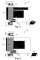
- the dielectric layer 12 may be deposited onto at least part of the bottom electrode 11. Different processes may be used for producing the dielectric layer 12, which processes may consist of different steps, comprising but not limited to, steps as for example sputtering or PECVD. Furthermore, the dielectric layer 12 may include holes and may have different shapes and sizes. In this embodiment, the dielectric layer 12 may cover the overlap area between an armature 13 and the bottom electrode 11 partially (Fig. 3) or completely (Fig. 4), the overlap area being defined by the projection of the armature 13 onto the bottom electrode 11 along a direction substantially perpendicular to plane of the bottom electrode 11 (i.e. the y-direction, see Fig.3 - 4).
- the projection of the dielectric layer 12 along the y-direction onto the bottom electrode 11 may also be shifted in a direction parallel to the plane of the bottom electrode 11 (i.e. the x-direction, see Fig.3 - 4).
- the dielectric layer 12 may also extend under the armature 13 and the geometry may preferably be such that a first part of the dielectric layer 12 is positioned at a first side of the armature 13 and a second part of the dielectric layer 12 is positioned at a second side of the armature 13, the first and second part of the armature 13 being positioned opposite to each other in a plane substantially perpendicular with the plane of the bottom electrode 11 (see Fig. 4).
- a floating electrode 14 is deposited onto at least part of the dielectric layer 12.
- the floating electrode 14 may consist essentially of a conductive material such as for example a metal (e.g. Au, Al or Cu), a semiconductor material (e.g. Si, Ge or GeAs) or a conductive polymer.
- the floating electrode 14 may be deposited by different suitable techniques, such as for example plating, sputtering, printing or spincoating.
- a low temperature process may be used in order not to affect the earlier deposited layers.
- the maximum allowed temperature depends on the type of materials used to form the dielectric layer 12 and/or the bottom electrode 11 and preferably may be less than 350°C or less than 250°C.
- the thickness of the floating electrode 14 may preferably be between 0.01 ⁇ m and 10 ⁇ m. More preferably the thickness may be between 0.1 ⁇ m and 2 ⁇ m. Most preferably the thickness of the floating electrode 14 may be between 0.1 ⁇ m and 0.3 ⁇ m.
- the floating electrode 14 may at least partially overlap with the armature 13 whereas the overlap between the armature 13 and the floating electrode 14 may be defined as the projection of the armature 13 onto the floating electrode 14 according to the y-direction (see Fig. 3 - 4).
- the part of the area situated under the armature 13, which is not covered by the floating electrode 14, may serve as actuation area, in particular interest the down state actuation area (see further).
- the geometry may preferably be such that a first part of the floating electrode 14 is positioned at a first side of the armature 13 and the bottom electrode 11 and a second part of the floating electrode 14 is positioned at a second side of the armature 13 and the bottom electrode 11, the first and second side of the armature 13 and the bottom electrode 11 being positioned opposite to each other in a plane substantially perpendicular with the plane of the bottom electrode 11.
- the floating electrode 14 may include holes 15 and 16, which may function as actuation area if the holes 15,16 overlap with the armature 13.
- the holes 15,16 may either partially or completely overlap with the holes in the dielectric layer 12.
- the surface of the floating electrode 14 may be made rough or patterned.
- the roughness of the surface of the floating electrode 14 may depend on the method of processing. Therefore, processing methods, which do not result in smooth surfaces, may be used to deposit the floating electrode 14.
- Another way to make the surface of the floating electrode 14 rougher may be by deposition of another conductive layer on top of the floating electrode by means of, for example, plating, sputtering, printing or spincoating.
- the floating electrode 14 may further comprise at least one elevated island (not shown in Fig. 3 and 4, see further) of conductive material such as for example a metal, a semiconductor material or a conductive polymer, whereby the island functions as a contactor between the armature 13 and the floating electrode 14.
- a sacrificial layer (not shown in Figures) may further be deposited on which, in a next step, the armature 13 may be formed.
- the sacrificial layer may for example be a polymer, such as for example BCB, polyimide or other suitable polymers used as photoresists in micorphotolithography and known to the skilled person.
- the thickness of the sacrificial layer determines the distance between the armature 13 and the floating electrode 14.
- the thickness of the sacrificial layer may be between 0.8 ⁇ m and 10 ⁇ m. More preferably the thickness may be between 1 ⁇ m and 5 ⁇ m. Most preferably the thickness of the sacrificial layer may be between 2 ⁇ m and 4 ⁇ m.
- the armature 13, which may be deposited on top of the sacrificial layer by for example sputtering, plating, printing or spincoating, may consist of for example a conductive material such as a metal (Au, Al, Cu or other suitable metals), a semiconductor material (Si, Ge, GeAs), a conductive polymer or any other suitable conductive material.
- the armature 13 and the floating electrode 14 may for example be formed out of the same material.
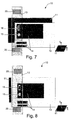
- actuation electrodes 17 are indicated.
- the actuation electrodes 17 may for example consist of a conductive material such as for example a metal, a semiconductor material or a conductive polymer, which may be different from the material of the bottom electrode 11 and the same of the material of the floating electrode 14, or which may, in another embodiment, both be different from the material of the bottom electrode 11 and different from the material of the floating electrode 14.
- an extra layer of dielectric material 18 may be deposited on top of at least some of the electrodes 14,17 in order to avoid direct contact with the armature 13 in the down state.
- the dielectric material 18 used to cover the different electrodes 14,17 may be different for each electrode 14,17.
- the up state actuation area 19 may be extended by the ar ea 20 of the actuation electrodes 17 as drawn in Fig. 7 and Fig. 8.
- the area 20 of the actuation electrodes 17 may also be contributed to the down state actuation area.
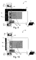
- the up state capacitance is determined by the up state actuation areas 19 (Fig. 5 and Fig. 6) while the down state capacitance is determined by the overlap 21 between the floating electrode 14 and bottom electrode 11 (Fig. 9 and Fig. 10).
- Overlap 21 may be defined by the projection of the floating electrode 14 onto the bottom electrode 11 along a direction substantially perpendicular to the plane of the bottom electrode 11.
- the total down state actuation area 22,23 may consist of the part of the area situated under the armature 13 which is not covered by the floating electrode 14 (Fig. 11) and may comprise, if actuation electrodes 17 are present, also area 20 of the actuation electrodes 17. In area 23 no supporting dielectric material and no floating electrode 14 are present. This means that, in that case, the dielectric material is air. In area 22 the dielectric material is giving support to the floating electrode 14.
- the actuation voltage to be applied between the armature 13 and up state actuation area 19 to cause the armature 13 to deform and contact the floating electrode 14 may preferably be between 1 V and 50 V or between -1 V and -50 V, but higher and lower values are not excluded. More preferably the voltage may between 4 V and 25 V or between -4 V and -25 V.
- the down/up capacitance ratio, C down /C up which is preferably as high as possible, is an important figure of merit quantifying the RF performance of a switch capacitance.
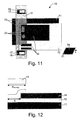
- Figure 12 shows a schematic view of a device 10 according to the present invention. The figure is only for the purpose of deriving the down/up capacitance ratio and is not limiting for the present invention.
- the down/up capacitance ratio may be determined as
- the first term of (eq. 4) may often be neglected because ⁇ r is negligible as there exists no good contact between the armature 13 and the dielectric layer 12.
- the down/up capacitance ration may then be defined by
- the down/up capacitance ratio may be increased by either increasing the area of the floating electrode 14 (A float ) or decreasing the overlap between the armature 13 and the signal line (see further) (A overlap ) or by both increasing A float and decreasing A overlap.
- the capacitance ratio was a limiting factor in the prior art, in the present invention it becomes a new variable of the device design.
- the capacitance ratio may be freely defined and precisely realized as it is defined by a contact with the top floating metal.
- the improvement may be especially important at low frequency, where the large down capacitance may be crucial.
- the device 10 of the present invention shows a separate dependence of up and down states, through which it becomes possible to improve one of the capacitances Cup or C down without influence the other one.
- overlap is meant the projection of the first part of the device onto the second part of the device along a direction substantially perpendicular to the plane of the bottom electrode 11.
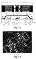
- FIG. 13 A preferred, but not limiting, embodiment of the present invention is shown in Fig. 13.
- FIG. 14 A corresponding SEM picture of the device 10, fabricated according to this preferred embodiment, is shown in Fig. 14.
- CPW ground lines 24 are introduced between the bottom electrode 11 and actuation electrodes 17.
- the processing of the device 10 may be described as follows.
- a stack constituting of a first conductive layer, a dielectric layer 12 and a second conductive layer is deposited onto a substrate 25.
- the first conductive layer may for example be a metal layer, such as e.g. Al or Cu, a semiconductor material, such as e.g. Si or Ge, or a conductive polymer, and may have a thickness of preferably 1 ⁇ m, but also conductive layers with another thickness, preferably between 0.1 ⁇ m and 10 ⁇ m, may be applied. From the first conductive layer, the bottom electrode 11 and CPW ground lines 24 will later be formed.
- the dielectric layer 12 may be made of for example an inorganic (e.g.Ta 2 O 5 ) or an organic (polymer) material and may preferably have a thickness between 0.01 ⁇ m and 100 ⁇ m, for example 0.2 ⁇ m.
- the second conductive layer may for example be a metal layer such as e.g. Al or Cu, or a conductive polymer and may preferably have a thickness between 0.01 ⁇ m and 10 ⁇ m, for example 0.1 ⁇ m.
- the floating electrode 14 will later on be formed from this second conductive layer.
- a substrate 25 for example an AF45 glass substrate may be used.
- Other suitable substrates may for example be, but are not limited to, glass, high resistive silicon or any low loss (or high resistive), not conductive material.
- a first mask is used to etch both the second conductive layer and the dielectric layer 12 to define where the first conductive layer has to be protected.
- a second mask is required to define the plate of the floating electrode 14.
- the 25/100/25 ⁇ m CPW ground lines 24 are defined using a third mask.
- a sacrificial layer which may for example be a polymer such as e.g. PCB, polyimide or other suitable polymers used as photoresists in standard photolithography and which may preferably have a thickness between 0.8 ⁇ m and 10 ⁇ m, for example 3 ⁇ m, is spincoated and patterned to define the bridge anchors 26.
- a polymer such as e.g. PCB, polyimide or other suitable polymers used as photoresists in standard photolithography and which may preferably have a thickness between 0.8 ⁇ m and 10 ⁇ m, for example 3 ⁇ m
- a third conductive layer which may for example be a metal layer, such as e.g. Al or Cu, a semiconductor material, such as e.g. Ge or Si, or a conductive polymer, may for example be sputtered or spincoated onto the device 10 and may be etched defining the armature 13 which in this preferred embodiment may have the shape of a bridge 27.
- the third conductive layer may have a thickness of for example 1 ⁇ m. The bridge 27 may then be released in a final sacrificial layer plasma etch.
- actuation electrodes 17 may be formed of the same conductive material as the bottom electrode 11. Furthermore, the dielectric material 18 on top of the actuation electrodes 17 may be the same as the dielectric material 18 covering the bottom electrode 11.
- the concept of using the floating electrode 14 is to ensure that an optimal down capacitance may be achieved without having to resort to very smooth surfaces. A few ohmic contact points between the bridge 27 and the floating electrode 14 suffice to attain the optimal down capacitance given by (eq. 2).
- the use of a floating electrode 14 furthermore allows the use of a thick highly conductive, and thus low-loss first conductive layer. The only requirement is that the contact impedance between the bridge 27 and the floating electrode 14 (combination of contact resistance and capacitance due to a native oxide layer) is sufficiently low, e.g. lower than 10 m ⁇ , preferably lower than 1 m ⁇ , so as not to limit the best attainable isolation.
- the up capacitance may be lowered without affecting the down capacitance.
- the overlap between the bridge 27 and the floating electrode 14 may be made as small as possible, e.g. smaller than for example 5 ⁇ m. This allows to further optimise the capacitance ratio.
- Fig. 13 and Fig. 14 provides actuation. This may be done in different ways which will be illustrated in the hereinafter described embodiments.
- the areas adjacent to the floating electrode 14, part of the switch capacitance and indicated as a first actuation area 28, are used.
- actuation is achieved by separate actuation electrodes 17 located in a second actuation area 29 adjacent to the signal line 30.
- a capacitive switch may result with the exception that a floating electrode 14 is used.
- the capacitive contact may be replaced by an ohmic contact.
- Fig. 15 to Fig. 24 Different embodiments of the present invention are represented schematically in Fig. 15 to Fig. 24. In all embodiments the production process of the different parts or layers may be performed as described before.
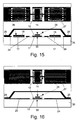
- FIG. 15 An embodiment of the present invention is depicted in Fig. 15.
- the architecture of the device is similar to that of Fig. 13 and Fig. 14, but the actuation electrodes 17 may be made of a different conductive material than the bottom electrode 11.
- the dielectric material 18 on top of the actuation electrodes 17 may be different from the dielectric layer 12 that is covering the bottom electrode 11.
- the thickness of the different layers and stacks of layers may be different.
- Fig. 16 another embodiment of the present invention is depicted.
- the device 10 comprises an armature which has the shape of a bridge 27. Down state actuation is performed by the areas adjacent to the floating electrode 14, part of the switch capacitance. There are no actuation electrodes 17 present. Hence, only the first actuation area 28 is present with respect to the previous embodiments.
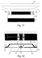
- An advantage of this embodiment with respect to the prior art is that because of the presence of the first actuation area 28, the bridge 27 will stay down after it has touched the floating electrode 14. In the prior art, the first actuation area 28 is not present and hence the bridge 27 will turn back to the up state position as soon as it has touched the floating electrode 14. This may be explained with respect to Fig. 17. The bridge 27 needs charge to stay in the down state position.
- FIG. 18 Yet another embodiment of the present invention is depicted in Fig. 18.
- the device is similar to that of Fig. 16, but the bridge 27 may have a less complex shape (top drawing of Fig. 18). Again, no actuation electrodes 17 and hence only the first actuation area 28 is present in the device 10 of this embodiment.
- This embodiment illustrates how the overlap between the bridge 27 and the floating electrode 14 may be made as small as possible, e.g. smaller than for example 5 ⁇ m, in order to reduce the up state capacitance (e.g. ⁇ 10cF) and hence to increase the capacitance ratio from (eq. 5).
- the up state capacitance e.g. ⁇ 10cF
- FIG. 19 Still another embodiment of the present invention is depicted in Fig. 19.
- the device may have a bridge 27 architecture and down state actuation may be performed by the first actuation areas 28, which are adjacent to the floating electrode 14, part of the switch capacitance. There are no actuation electrodes 17, and hence no second actuation area 29.
- the floating electrode 14 may consist of two parts C and C'. Between the two parts C and C' the dielectric layer 12 may be interrupted.
- An advantage of the dielectric layer 12 being interrupted is the floating electrode 14 may be used as a mask to etch the dielectric layer 14, hereby reducing the number of masking steps necessary during the processing of the device 10 of the present invention.
- the dielectric layer 12 may be charged due to the actuation voltage. Therefore, the dielectric layer 12 may be interrupted at the place where no floating electrode 14 is present. Hence, the dielectric material then present is vacuum, which does not charge very easily.
- the bridge 27 in this embodiment may have the same shape as in the previous embodiment (Fig. 18), hence the overlap between the bridge 27 and the floating electrode 14 is small and thus the up state capacitance is small too, preferably smaller than 10 cF.
- Reference number 31 in Fig. 19 represents the bridge in deformed state.
- FIG. 20 A further embodiment of the present invention is depicted in Fig. 20.
- This embodiment is similar to the previous embodiment (Fig. 19).
- the device may have a bridge 27 architecture and down state actuation may be performed by the first actuation area 28, adjacent to the floating electrode 14, part of the switch capacitance.
- the floating electrode 14 may consist of two parts C and C' and the bridge 27 may have the same shape as in the two previous embodiments.
- the up state capacitance is small (preferably ⁇ 10 cF), and the down/up capacitance ratio is increased.
- the difference between this embodiment and the previous one is that between the two parts C and C' the dielectric layer 12 now may be present.
- the force exercised on the bridge 27 is decreased in the areas 31 b due to charging of the floating electrode 14. Between C and C', in the area 31 a the force remains and hence the bridge 27 will stay in the down state position. Important in this embodiment is to use a dielectric layer 12 which does not charge easily. Otherwise, if the dielectric layer 12 is charged due to the actuation voltage, the force exercised on the bridge 27 will be reduced and the bridge 27 may bounce back to the up state positon.
- the device 10 of the present invention comprises an armature which has the shape of a bridge 27.
- the above described devices 10 are shunt switches.
- the armature may have the shape of a cantilever 32 and thus in the following embodiments, series switches are discussed.
- the armature may have the shape of a cantilever 32.
- Down state actuation may be performed by the first actuation area 28 adjacent to the floating electrode 14 and/or by one actuation electrode 17, and thus the second actuation area 29.
- Both actuation electrode 17 and floating electrode 14 may be situated under the cantilever 32.
- Reference number 33 represents the cantilever 32 in the deformed state.
- the overlap between the floating electrode 14 and the cantilever 32 may be made as small as possible (e.g. ⁇ 5 ⁇ m) in order to decrease Cup (e.g. ⁇ 10 cF) and only the actuation electrode 17 may be situated under the cantilever 32.
- Down state actuation may be performed by one actuation electrode 17. Only the second actuation area 29 is present. This is different from the previous embodiment, where actuation may be performed by both the first 28 and the second 29 actuation area.
- the device may have a cantilever 32 architecture and down state actuation may be performed by the first actuation area 28 adjacent to the floating electrode 14, situated under the cantilever 32.
- the overlap between the floating electrode 14 and the cantilever 32 may be made as small as possible, preferably smaller than 5 ⁇ m, again to make the upstate capacitance as close to zero as possible (preferably ⁇ 10 cF).
- No actuation electrode 17 is present.
- the first actuation area 28 may much larger with respect to the previous embodiments.
- the down state position of the cantilever 32 may be very stable for reasons already explained with respect to Fig. 17.
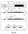
- a superincumbent island 34 of a conductive material may be deposited onto a part of the dielectric layer 12 which is not covered with the floating electrode 14, in order to reduce or avoid stiction.
- the superincumbent island 34 may be made of for example a metal such as Cu, Al, Au or may be any other suitable conductive material.
- FIG. 25 A further embodiment of the present invention is depicted in Fig. 25.
- the device is similar to Fig. 24, but now more then one superincumbent island 34 of conductive material such as for example Cu, Al, Au, or any other suitable conductive material, may be present.
- the different superincumbent islands 34 may be of different shapes and formed out of different materials.
- the down surface of the cantilever 32 may comprise at least one elevated island in order to reduce stiction between the cantilever 32 and the floating electrode.
- the floating electrode 14 may be embedded or encapsulated within the dielectric layer 12.
Abstract
Description
- The present invention relates to electronic devices, especially micro electromechanical (MEMS) devices and method of making the same. In particular the present invention relates to the field of radio frequency MEMS and more particularly the present invention relates to MEMS near-DC to RF capacitive shunt and series switches, e.g. a switchable capacitor.
- RF-MEMS switches offer great potential benefits over GaAs MMICs and PIN (positive intrinsic negative) diode switches for application in wireless communication systems as is described by C. T.-G. Nguyen, et al., in "Micromachined devices for wireless communications", Proc. of the IEEE, vol. 86(8), 1998, pp. 1756-1768, by J. J. Yao, in "RF MEMS from a device perspective", J. Micromech. Microeng., vol.10(4), December 2000, pp. R9-R38 and by G. M. Rebeiz and J. B. Muldavin, in "RF MEMS switches and switch circuits", IEEE Microwave magazine, Dec. 2001, pp. 59-71. Prototype RF-MEMS switches display low loss (<0.4 dB), good isolation (>20 dB), extremely low standby power consumption, excellent linearity (IP3>66dBm), compactness and high levels of integration as discussed by J. J. Yao, in "RF MEMS from a device perspective", J. Micromech. Microeng., vol.10(4), December 2000, pp. R9-R38, by G. M. Rebeiz and J. B. Muldavin, in "RF MEMS switches and switch circuits", IEEE Microwave magazine, Dec. 2001, pp. 59-71, by Z. J. Yao, et al., in "Micromachined low-loss microwave switches", IEEE J. of MEMS, vol. 8(2), 1999, pp. 129-134, by J. B. Muldavin and G. M. Rebeiz, in "High-isolation CPW MEMS shunt switches-Part 1: Modeling", IEEE Trans. Microwave Theory and Techniques, vol. 48(6), 2000, pp. 1045-1052 and by H. A. C. Tilmans, et al., in "Wafer-level packaged RF-MEMS switches fabricated in a CMOS fab", proc. IEDM 2001, Washington, DC, December 3-5, 2001, pp. 921-924'.
- A typical build-up of a RF-MEMS capacitive switch in a shunt configuration implemented on a CPW (CoPlanar Waveguide) line is shown in Fig. 1 and has been discussed in by Z. J. Yao, et al., in "Micromachined low-loss microwave switches", IEEE J. of MEMS, vol. 8(2), 1999, pp. 129-134, by J. B. Muldavin and G. M. Rebeiz, in "High-isolation CPW MEMS shunt switches-Part 1: Modeling", IEEE Trans. Microwave Theory and Techniques, vol. 48(6), 2000, pp. 1045-1052 and by H. A. C. Tilmans, et al., in "Wafer-level packaged RF-MEMS switches fabricated in a CMOS fab", proc. IEDM 2001, Washington, DC, December 3-5, 2001, pp. 921-924. The switch consists of a suspended movable metal bridge, which is mechanically anchored and electrically connected to the ground of the CPW.
- To a first order, the switch can be modeled as a capacitor between the metal bridge and the signal line. In the RF-ON state the bridge is up, hence the switch capacitance is small, hardly affecting the impedance of the line. By applying a DC. bias (superimposed on the RF signal) the bridge is pulled down onto the dielectric, the switch capacitance becomes high and the switch is OFF or in the isolation state. An important figure of merit quantifying the RF performance is the down/up capacitance ratio, Cdown/Cup, which is preferably as high as possible. This ratio can be approximated bywhere dair and ddiel are the thickness of the air gap and the dielectric, respectively, εr is the dielectric constant of the dielectric and Aoverlap is the overlap area of the bridge and the signal line. For a given technology, as Aoverlap cancels in (eq. 1), the isolation determines the insertion loss and vice versa. The design freedom is thus constrained considerably.

- A second problem encountered in capacitive switches of the type shown in Fig. 1 is the degradation of the effective down capacitance as a result of surface roughness preventing intimate contact between the beam and the dielectric, which is discussed by J. B. Muldavin and G. M. Rebeiz in "High-isolation CPW MEMS shunt switches-Part 1: Modeling", IEEE Trans. Microwave Theory and Techniques, vol. 48(6), 2000, pp. 1045-1052. Solutions commonly pursued to attain a large down capacitance are aimed at keeping the roughness of the bridge and of the dielectric layer very low, e.g., <5 nm, and to keep the surface free from residues. Muldavin et al. and Yao et al. introduced thin bottom metals in an attempt to reduce the roughness. In particular, Z.J. Yao et al. described in "Micromachined low-loss microwave switches", IEEE J. of MEMS, vol. 8(2), 1999, pp. 129-134, the use of a thin refractory metal layer (e.g., W). All these measures however lead to a high series resistance and hence to an increased insertion loss for a shunt switch. Obviously, in a standard design as the one shown in Fig. 1, a difficult compromise must be made as measures for improving the isolation directly lead to a deterioration of the insertion loss.
- In PCT patent application WO 02/01584, "Capacitive Micro electromechanical switches" by R. York et al., a micro electromechanical switch (Fig. 2) is disclosed comprising a
bottom electrode 1, adielectric layer 2 disposed on thebottom electrode 1, a metal cap (not shown) disposed on thedielectric layer 2 and abridge 3 disposed proximate to the metal cap such that an electrical potential applied between thebridge 3 andbottom electrode 1 causes thebridge 3 to deform and contact the metal cap. The deformed bridge is depicted withreference number 4. A problem with this device is that charging of the metal cap will reduce the force exercised on thebridge 3, which might bounce back into the original position, hereby disturbing the normal working of the switch. - It is an object of the present invention is to provide an electronic device and method of manufacture of the same which a) has an acceptable insertion loss, and/or b) do not require ultra-smooth surfaces and/or c) do not have an unacceptable bounce back.
- The present invention is applicable in the field of switchable capacitors and capacitive switches. The present invention provides a micro electromechanical switchable capacitor, a shunt switch or a series switch (corresponding to bridge and cantilever) with relay actuation or actuation in zones attached to a floating electrode area.
- In a first aspect of the invention a micro electromechanical switchable capacitor is disclosed, comprising a substrate, a bottom electrode, a dielectric layer deposited on at least part of the bottom electrode, a conductive floating electrode deposited on at least part of the dielectric layer, an armature positioned proximate to the floating electrode so as to form an overlap with the floating electrode, the overlap being defined by projection of the armature onto the floating electrode along a direction substantially perpendicular to the plane of the bottom electrode. Furthermore, the switchable capacitor of the present invention comprises a first actuation area, which is defined by a part of an overlap between the armature and the bottom electrode which is not covered by the floating electrode, the overlap between the armature and the bottom electrode being defined by projection of the armature onto the bottom electrode along a direction substantially perpendicular to the bottom electrode. An advantage of the device of the present invention is that, because of the first actuation area, the armature remains in the down state position after touching the floating electrode.
- In a preferred embodiment the switchable capacitor of the present invention may furthermore comprise at least one actuation electrode and a second actuation area, which second actuation area may be defined by an overlap between the armature and the at least one actuation electrode, the overlap being defined by projection of the armature onto the bottom electrode in a direction substantially perpendicular to the plane of the bottom electrode. Through the presence of the second actuation area, stability of the down state position of the armature is increased.
- In one embodiment of the present invention, the overlap between the floating electrode and the armature, which overlap is defined by projection of the armature onto the floating electrode in a direction substantially perpendicular to the plane of the bottom electrode, may be made as small as possible in order to decrease the up state capacitance and hence increase the down/up capacitance ratio.
- The capacitor comprises a first and a second side opposite to each other in a plane substantially parallel to the plane of the bottom electrode. The armature may be located such that a first part of the floating electrode is positioned at the first side of the armature and a second part of the floating electrode is positioned at the second side of the armature.
- In the present invention, the armature may be a bridge or a cantilever.
- An up state actuation area may be defined by the overlap between the armature and the bottom electrode and/or by the second actuation area.
- A down state actuation area may be defined by the first actuation area and/or by the second actuation area.
- In another embodiment of the present invention, Cup may be defined as the up state capacitance which may be a function of the overlap area between the armature and the bottom electrode. In a further embodiment the up state capacitance may be proportional with the overlap between the armature and the bottom electrode.
- In yet another embodiment the up state capacitance may be made as low as possible, in order to increase the down/up capacitance ratio, by reducing the overlap between the armature and the bottom electrode.
- In an embodiment of the present invention, Cdown may be defined as the down state capacitance which may be a function of the overlap area between the floating electrode and the bottom electrode, which overlap may be defined by projection of the floating electrode onto the bottom electrode according to a direction substantially perpendicular to the plane of the bottom electrode. In a further embodiment the down state capacitance may be proportional with the overlap between the floating electrode and the bottom electrode.
- In an embodiment of the present invention the floating electrode may consist of two or more unconnected regions. In another embodiment of the present invention, each of the unconnected regions may have an overlap with the armature, the overlap being defined by projection of the armature onto the unconnected regions of the floating electrode according to a direction substantially perpendicular to the plane of the bottom electrode.
- In a further embodiment of the present invention at least one superincumbent island of conductive material may be deposited on the floating electrode. The at least one superincumbent island functions as a contactor between the armature and the floating electrode.
- In an embodiment of the present invention, the armature, comprising an up and down surface positioned opposite of each other in a plane substantially perpendicular to the plane of the bottom electrode, may comprise on its down surface at least one superincumbent island of conductive material. The at least one supericumbent island functions as contactor between the armature and the floating electrode.
- In a further embodiment of the present invention the floating electrode may be embedded or encapsulated in the dielectric layer.
- In another embodiment of the present invention the dielectric layer may comprise holes. In still another embodiment the floating electrode may comprise holes. In yet another embodiment the armature may comprise holes.
- The present invention also provides a method for processing a micro electromechanical switchable capacitor, the method comprising :
- depositing of a stack comprising a first conductive layer, a second conductive layer and a first dielectric layer in between said first and said second conductive layer,
- etching said second conductive layer and said first dielectric layer using a first mask, so as to define a region of the first conductive layer that is protected by the first mask,
- etching said second conductive layer using a second mask, so as to form a floating electrode and a first actuation area,
- etching said first conductive layer using a third mask, so as to form a bottom electrode and ground lines, and
- depositing and etching a third conductive layer so as to form an armature.
-
- The method may further comprise depositing and patterning a sacrificial layer before depositing the third conductive layer, and etching said sacrificial layer so as to release said armature. The method may furthermore comprise:
- depositing a second dielectric material, and etching said second dielectric material and said first conductive layer so as to form actuation electrodes. The armature can be a bridge or cantilever. The method may furthermore comprise depositing at least one superincumbent island onto said floating electrode. Holes may be provided in said dielectric layer and/or in said floating electrode and/or in said armature.
-
- An advantage of the present invention is that by modifying the geometry of the device of the present invention, it is possible to increase the down/up capacitance ratio, which ratio is an important feature of a switchable capacitor.
- These and other characteristics, features and advantages of the present invention will become apparent from the following detailed description, taken in conjunction with the accompanying drawings, which illustrate, by way of example, the principles of the invention. This description is given for the sake of example only, without limiting the scope of the invention. The reference figures quoted below refer to the attached drawings.
-
- Fig. 1 shows a prior art RF-MEMS capacitive shunt switch.
- Fig. 2 illustrates an embodiment related to the invention described in PCT Patent application No. WO 02/01584.
- Fig. 3 - 11 illustrate various relevant parts of an embodiment of the present invention.
- Fig. 12 is a schematic representation of the device of an embodiment of the present invention.
- Fig. 13 shows an RF MEMS capacitive switch structure according to a preferred embodiment of the invention.
- Fig. 14 is a SEM picture of the RF MEMS switching device of Fig. 13.
- Fig. 15-16 and 18-24 show RF MEMS capacitive switch structures according to different embodiments of the invention.
- Fig. 17 is a schematic representation of a further embodiment of the present invention.
-
- The present invention will be described with respect to particular embodiments and with reference to certain drawings but the invention is not limited thereto but only by the claims. The drawings described are only schematic and are non-limiting. In the drawings, the size of some of the elements may be exaggerated and not drawn on scale for illustrative purposes. Where the term "comprising" is used in the present description and claims, it does not exclude other elements or steps.
- Furthermore, the terms first, second, third and the like in the description and in the claims, are used for distinguishing between similar elements and not necessarily for describing a sequential or chronological order. It is to be understood that the terms so used are interchangeable under appropriate circumstances and that the embodiments of the invention described herein are capable of operation in other sequences than described or illustrated herein.
- Moreover, the terms top, bottom, over, under and the like in the description and the claims are used for descriptive purposes and not necessarily for describing relative positions. It is to be understood that the terms so used are interchangeable under appropriate circumstances and that the embodiments of the invention described herein are capable of operation in other orientations than described or illustrated herein.
- The present invention provides embodiments for shunt switches and series switches which have corresponding features of a bridge and a cantilever respectively), with relay actuation or actuation in zones attached to the floating electrode area, and provides devices for application in the field of switchable capacitors and capacitive switches.
- For the purpose of the description of the present invention, different relevant generic parts of the device are defined by reference to Figs. 3 - 11, wherein different implementations of the present invention are illustrated. The relative dimensions of the different parts may be chosen as a function of the required working phase space and characteristics of the device, though preferred value ranges will be mentioned.
- The
device 10 according to the present invention is formed onto a substrate, which may for example be, but is not limited to, glass, high resistive semiconductors, ceramic materials, or any low loss, non-conductive material. With low loss is meant that the substrate may have a loss tangent which is smaller than 1e-4. For clarity reasons, the substrate is not depicted in Fig. 3 to Fig. 11. - In general the value of capacitance depends on the type of dielectric material used to insulate a capacitor. Air may is also a dielectric material for the purpose of this invention, though generally only in combination with another dielectric material that is providing support to a floating electrode. Furthermore, the dielectric material may also be provided by a vacuum.
- Fig. 3 - 11 illustrate the
device 10 of the present invention, showing the following parts. Abottom electrode 11, which may be in a coplanar waveguide (CPW) line corresponding to a signal line (not shown in figures 3 - 11), may consist of a conductive material such as for example a metal, a semiconductor material or a conductive polymer. Any suitable singal feeding system may be used, e.g. besides a CPW geometry, also microstrip, stripline or CPW with grounded backside geometries may be used. Thebottom electrode 11 may be produced by means of suitable techniques for the deposition of a conductive material such as for instance, but not limited to, sputtering, plating, printing or spincoating. The thickness of thebottom electrode 11, as well as the ground lines present in some of the preferred embodiments of the invention (see further), may preferably be between 0.1 µm and 10 µm and more preferably the thickness of thebottom electrode 11 may be between 1 µm and 3 µm. - Furthermore, the
device 10 of the present invention comprises adielectric layer 12, which may consist of a dielectric material such as for example, but not limited to, inorganic (SiO2, Ta2O5 Si3N4) or organic (polymer) materials. Thedielectric layer 12 may preferably have a thickness between 0.01 µm and 100 µm. More preferably thedielectric layer 12 may have a thickness between 0.01 µm and 10 µm. Most preferably thedielectric layer 12 may have a thickness between 0.1 µm and 1 µm. In order to increase the down state capacitance (see further), athin dielectric layer 12 may be preferred over a thick one. Thedielectric layer 12 may however not be too thin in order to avoid breakdown of the capacitor. Breakdown of the capacitor depends on the material used to form thedielectric layer 12 and on the applied voltage. Therefore, the minimum allowable thickness to avoid breakdown of the capacitor depends on the material used to form thedielectric layer 12. Typical breakdown voltages are in the order of 1e8 - 1 e9 volts per meter. - The
dielectric layer 12 may be deposited onto at least part of thebottom electrode 11. Different processes may be used for producing thedielectric layer 12, which processes may consist of different steps, comprising but not limited to, steps as for example sputtering or PECVD. Furthermore, thedielectric layer 12 may include holes and may have different shapes and sizes. In this embodiment, thedielectric layer 12 may cover the overlap area between anarmature 13 and thebottom electrode 11 partially (Fig. 3) or completely (Fig. 4), the overlap area being defined by the projection of thearmature 13 onto thebottom electrode 11 along a direction substantially perpendicular to plane of the bottom electrode 11 (i.e. the y-direction, see Fig.3 - 4). The projection of thedielectric layer 12 along the y-direction onto thebottom electrode 11 may also be shifted in a direction parallel to the plane of the bottom electrode 11 (i.e. the x-direction, see Fig.3 - 4). Thedielectric layer 12 may also extend under thearmature 13 and the geometry may preferably be such that a first part of thedielectric layer 12 is positioned at a first side of thearmature 13 and a second part of thedielectric layer 12 is positioned at a second side of thearmature 13, the first and second part of thearmature 13 being positioned opposite to each other in a plane substantially perpendicular with the plane of the bottom electrode 11 (see Fig. 4). - In a next step, a floating
electrode 14 is deposited onto at least part of thedielectric layer 12. The floatingelectrode 14 may consist essentially of a conductive material such as for example a metal (e.g. Au, Al or Cu), a semiconductor material (e.g. Si, Ge or GeAs) or a conductive polymer. The floatingelectrode 14 may be deposited by different suitable techniques, such as for example plating, sputtering, printing or spincoating. Preferably a low temperature process may be used in order not to affect the earlier deposited layers. The maximum allowed temperature depends on the type of materials used to form thedielectric layer 12 and/or thebottom electrode 11 and preferably may be less than 350°C or less than 250°C. The thickness of the floatingelectrode 14 may preferably be between 0.01 µm and 10 µm. More preferably the thickness may be between 0.1 µm and 2 µm. Most preferably the thickness of the floatingelectrode 14 may be between 0.1 µm and 0.3 µm. - The floating
electrode 14 may at least partially overlap with thearmature 13 whereas the overlap between thearmature 13 and the floatingelectrode 14 may be defined as the projection of thearmature 13 onto the floatingelectrode 14 according to the y-direction (see Fig. 3 - 4). The part of the area situated under thearmature 13, which is not covered by the floatingelectrode 14, may serve as actuation area, in particular interest the down state actuation area (see further). The geometry may preferably be such that a first part of the floatingelectrode 14 is positioned at a first side of thearmature 13 and thebottom electrode 11 and a second part of the floatingelectrode 14 is positioned at a second side of thearmature 13 and thebottom electrode 11, the first and second side of thearmature 13 and thebottom electrode 11 being positioned opposite to each other in a plane substantially perpendicular with the plane of thebottom electrode 11. The floatingelectrode 14 may includeholes holes armature 13. Theholes dielectric layer 12. In order to reduce stiction between thearmature 13 and the floatingelectrode 14 in the down state, the surface of the floatingelectrode 14 may be made rough or patterned. The roughness of the surface of the floatingelectrode 14 may depend on the method of processing. Therefore, processing methods, which do not result in smooth surfaces, may be used to deposit the floatingelectrode 14. Another way to make the surface of the floatingelectrode 14 rougher may be by deposition of another conductive layer on top of the floating electrode by means of, for example, plating, sputtering, printing or spincoating. For the same reason, i.e. to reduce stiction, and for a second reason, i.e. to reduce the distance between thearmature 13 and the floatingelectrode 14, the floatingelectrode 14 may further comprise at least one elevated island (not shown in Fig. 3 and 4, see further) of conductive material such as for example a metal, a semiconductor material or a conductive polymer, whereby the island functions as a contactor between thearmature 13 and the floatingelectrode 14. - On top of this structure a sacrificial layer (not shown in Figures) may further be deposited on which, in a next step, the
armature 13 may be formed. The sacrificial layer may for example be a polymer, such as for example BCB, polyimide or other suitable polymers used as photoresists in micorphotolithography and known to the skilled person. The thickness of the sacrificial layer determines the distance between thearmature 13 and the floatingelectrode 14. Preferably the thickness of the sacrificial layer may be between 0.8 µm and 10 µm. More preferably the thickness may be between 1 µm and 5 µm. Most preferably the thickness of the sacrificial layer may be between 2 µm and 4 µm. - The
armature 13, which may be deposited on top of the sacrificial layer by for example sputtering, plating, printing or spincoating, may consist of for example a conductive material such as a metal (Au, Al, Cu or other suitable metals), a semiconductor material (Si, Ge, GeAs), a conductive polymer or any other suitable conductive material. Thearmature 13 and the floatingelectrode 14 may for example be formed out of the same material. Thearmature 13 and the floatingelectrode 14 may, however, also be formed out of different materials. In the latter case, stiction between thearmature 13 and the floatingelectrode 14 in the down state will be reduced. Openings in thearmature 13 may be formed by means of for example an etching process. During the same etching process the sacrificial layer may be removed. - Furthermore, in Fig. 3 and Fig. 4,
actuation electrodes 17 are indicated. Theactuation electrodes 17 may for example consist of a conductive material such as for example a metal, a semiconductor material or a conductive polymer, which may be different from the material of thebottom electrode 11 and the same of the material of the floatingelectrode 14, or which may, in another embodiment, both be different from the material of thebottom electrode 11 and different from the material of the floatingelectrode 14. Furthermore, an extra layer ofdielectric material 18 may be deposited on top of at least some of theelectrodes armature 13 in the down state. Thedielectric material 18 used to cover thedifferent electrodes electrode - In Fig. 5 and Fig. 6 an up
state actuation area 19, which may be extended if there areactuation electrodes 17 present, is defined as the overlap between thearmature 13 and thebottom electrode 11, whereas the overlap is defined by the projection of thearmature 13 onto thebottom electrode 11 according to a direction substantially perpendicular to the plane of thebottom electrode 11. The upstate actuation area 19 may be extended by thear ea 20 of theactuation electrodes 17 as drawn in Fig. 7 and Fig. 8. Thearea 20 of theactuation electrodes 17 may also be contributed to the down state actuation area. - The up state capacitance is determined by the up state actuation areas 19 (Fig. 5 and Fig. 6) while the down state capacitance is determined by the
overlap 21 between the floatingelectrode 14 and bottom electrode 11 (Fig. 9 and Fig. 10).Overlap 21 may be defined by the projection of the floatingelectrode 14 onto thebottom electrode 11 along a direction substantially perpendicular to the plane of thebottom electrode 11. The total downstate actuation area armature 13 which is not covered by the floating electrode 14 (Fig. 11) and may comprise, ifactuation electrodes 17 are present, alsoarea 20 of theactuation electrodes 17. Inarea 23 no supporting dielectric material and no floatingelectrode 14 are present. This means that, in that case, the dielectric material is air. Inarea 22 the dielectric material is giving support to the floatingelectrode 14. - The actuation voltage to be applied between the
armature 13 and upstate actuation area 19 to cause thearmature 13 to deform and contact the floatingelectrode 14 may preferably be between 1 V and 50 V or between -1 V and -50 V, but higher and lower values are not excluded. More preferably the voltage may between 4 V and 25 V or between -4 V and -25 V. - As already discussed in the prior art section, the down/up capacitance ratio, Cdown/Cup, which is preferably as high as possible, is an important figure of merit quantifying the RF performance of a switch capacitance. Figure 12 shows a schematic view of a
device 10 according to the present invention. The figure is only for the purpose of deriving the down/up capacitance ratio and is not limiting for the present invention. The down capacitance may be defined byarmature 13 and a signal line (see further). The up state capacitance may be defined by - By dividing (eq. 2) by (eq. 3) the down/up capacitance ratio may be determined as

- The first term of (eq. 4) may often be neglected because εr is negligible as there exists no good contact between the
armature 13 and thedielectric layer 12. The down/up capacitance ration may then be defined by
- An important difference between the above equation (eq. 5) and the equation derived for the switch capacitance of the prior art (eq. 1) is the factor (Afloat/Aoverlap) which is called the geometrical factor. By modifying this geometrical factor, i.e. by changing Afloat and/or Aoverlap and hence modifying the geometry of the
device 10, it is possible to reach a large capacitance ratio, for example, for thedevice 10 of the present invention, a capacitance ratio of more than 600 may be achieved. From (eq. 5) it becomes clear that the down/up capacitance ratio may be increased by either increasing the area of the floating electrode 14 (Afloat) or decreasing the overlap between thearmature 13 and the signal line (see further) (Aoverlap) or by both increasing Afloat and decreasing Aoverlap. - As the capacitance ratio was a limiting factor in the prior art, in the present invention it becomes a new variable of the device design. The capacitance ratio may be freely defined and precisely realized as it is defined by a contact with the top floating metal. The improvement may be especially important at low frequency, where the large down capacitance may be crucial. The
device 10 of the present invention shows a separate dependence of up and down states, through which it becomes possible to improve one of the capacitances Cup or Cdown without influence the other one. - Whenever in the further description, the following embodiments and/or in the claims overlap between two parts of the device of the present invention is mentioned, by overlap is meant the projection of the first part of the device onto the second part of the device along a direction substantially perpendicular to the plane of the
bottom electrode 11. - A preferred, but not limiting, embodiment of the present invention is shown in Fig. 13. A corresponding SEM picture of the
device 10, fabricated according to this preferred embodiment, is shown in Fig. 14. In this preferred embodiment, CPW ground lines 24 are introduced between thebottom electrode 11 andactuation electrodes 17. - The processing of the
device 10 according to this preferred embodiment of the present invention may be described as follows. A stack constituting of a first conductive layer, adielectric layer 12 and a second conductive layer is deposited onto asubstrate 25. The first conductive layer may for example be a metal layer, such as e.g. Al or Cu, a semiconductor material, such as e.g. Si or Ge, or a conductive polymer, and may have a thickness of preferably 1 µm, but also conductive layers with another thickness, preferably between 0.1 µm and 10 µm, may be applied. From the first conductive layer, thebottom electrode 11 and CPW ground lines 24 will later be formed. Thedielectric layer 12 may be made of for example an inorganic (e.g.Ta2O5) or an organic (polymer) material and may preferably have a thickness between 0.01 µm and 100 µm, for example 0.2 µm. The second conductive layer may for example be a metal layer such as e.g. Al or Cu, or a conductive polymer and may preferably have a thickness between 0.01 µm and 10 µm, for example 0.1 µm. The floatingelectrode 14 will later on be formed from this second conductive layer. As asubstrate 25, for example an AF45 glass substrate may be used. Other suitable substrates may for example be, but are not limited to, glass, high resistive silicon or any low loss (or high resistive), not conductive material. - A first mask is used to etch both the second conductive layer and the
dielectric layer 12 to define where the first conductive layer has to be protected. A second mask is required to define the plate of the floatingelectrode 14. The 25/100/25µm CPW ground lines 24 are defined using a third mask. - Next, a sacrificial layer, which may for example be a polymer such as e.g. PCB, polyimide or other suitable polymers used as photoresists in standard photolithography and which may preferably have a thickness between 0.8 µm and 10 µm, for example 3 µm, is spincoated and patterned to define the bridge anchors 26.
- Furthermore, a third conductive layer, which may for example be a metal layer, such as e.g. Al or Cu, a semiconductor material, such as e.g. Ge or Si, or a conductive polymer, may for example be sputtered or spincoated onto the
device 10 and may be etched defining thearmature 13 which in this preferred embodiment may have the shape of abridge 27. The third conductive layer may have a thickness of for example 1 µm. Thebridge 27 may then be released in a final sacrificial layer plasma etch. - In this preferred embodiment,
actuation electrodes 17 may be formed of the same conductive material as thebottom electrode 11. Furthermore, thedielectric material 18 on top of theactuation electrodes 17 may be the same as thedielectric material 18 covering thebottom electrode 11. - The concept of using the floating
electrode 14 is to ensure that an optimal down capacitance may be achieved without having to resort to very smooth surfaces. A few ohmic contact points between thebridge 27 and the floatingelectrode 14 suffice to attain the optimal down capacitance given by (eq. 2). The use of a floatingelectrode 14 furthermore allows the use of a thick highly conductive, and thus low-loss first conductive layer. The only requirement is that the contact impedance between thebridge 27 and the floating electrode 14 (combination of contact resistance and capacitance due to a native oxide layer) is sufficiently low, e.g. lower than 10 mΩ, preferably lower than 1 mΩ, so as not to limit the best attainable isolation. By choosing abridge 27 which is more narrow than the floatingelectrode 14, and hence reducing the overlap between thebridge 27 and the floatingelectrode 14, the up capacitance may be lowered without affecting the down capacitance. The overlap between thebridge 27 and the floatingelectrode 14 may be made as small as possible, e.g. smaller than for example 5 µm. This allows to further optimise the capacitance ratio. - The introduction of the floating
electrode 14 requires a revision of the actuation scheme of the standard switch of prior art Fig. 1. Just covering thedielectric layer 12 with a floating electrode would result in anunstable device 10 because if, in this case, a bias is applied, thebridge 27 pulls in but releases as soon as it touches the floatingelectrode 14. Upon contact, the floatingelectrode 14 and thebridge 27 have the same potential. In other words, the electrostatic attractive force vanishes. The same happens in the prior art device of Fig. 2 where a metal cap is positioned onto thedielectric layer 2 in order to make contact with thebridge 3. When thebridge 3 touches the metal cap, the forces exercised on thebridge 3 will be reduced because of charging of the metai cap. - Therefore, the structure shown in Fig. 13 and Fig. 14 provides actuation. This may be done in different ways which will be illustrated in the hereinafter described embodiments. In one embodiment the areas adjacent to the floating
electrode 14, part of the switch capacitance and indicated as afirst actuation area 28, are used. In another embodiment actuation is achieved byseparate actuation electrodes 17 located in asecond actuation area 29 adjacent to thesignal line 30. In using the first actuation area 28 a capacitive switch may result with the exception that a floatingelectrode 14 is used. Using thesecond actuation area 29, the capacitive contact may be replaced by an ohmic contact. - Different embodiments of the present invention are represented schematically in Fig. 15 to Fig. 24. In all embodiments the production process of the different parts or layers may be performed as described before.
- An embodiment of the present invention is depicted in Fig. 15. The architecture of the device is similar to that of Fig. 13 and Fig. 14, but the
actuation electrodes 17 may be made of a different conductive material than thebottom electrode 11. Furthermore, thedielectric material 18 on top of theactuation electrodes 17 may be different from thedielectric layer 12 that is covering thebottom electrode 11. Also the thickness of the different layers and stacks of layers may be different. - In Fig. 16 another embodiment of the present invention is depicted. The
device 10 comprises an armature which has the shape of abridge 27. Down state actuation is performed by the areas adjacent to the floatingelectrode 14, part of the switch capacitance. There are noactuation electrodes 17 present. Hence, only thefirst actuation area 28 is present with respect to the previous embodiments. An advantage of this embodiment with respect to the prior art is that because of the presence of thefirst actuation area 28, thebridge 27 will stay down after it has touched the floatingelectrode 14. In the prior art, thefirst actuation area 28 is not present and hence thebridge 27 will turn back to the up state position as soon as it has touched the floatingelectrode 14. This may be explained with respect to Fig. 17. Thebridge 27 needs charge to stay in the down state position. As in WO 02/01584, nofirst actuation area 28 is present, charging of the metal cap will reduce the force exercised on thebridge 27. Hence, thebridge 27 bounces back to the up state position. In this embodiment of the present invention, the charging of the floatingelectrode 14 will also reduce the force on thedeformed bridge 31, but in thefirst actuation area 28 this force, which is indicated by the arrows, remains and hence thebridge 27 stays in the down state position. - Yet another embodiment of the present invention is depicted in Fig. 18. The device is similar to that of Fig. 16, but the
bridge 27 may have a less complex shape (top drawing of Fig. 18). Again, noactuation electrodes 17 and hence only thefirst actuation area 28 is present in thedevice 10 of this embodiment. This embodiment illustrates how the overlap between thebridge 27 and the floatingelectrode 14 may be made as small as possible, e.g. smaller than for example 5 µm, in order to reduce the up state capacitance (e.g. < 10cF) and hence to increase the capacitance ratio from (eq. 5). - Still another embodiment of the present invention is depicted in Fig. 19. The device may have a
bridge 27 architecture and down state actuation may be performed by thefirst actuation areas 28, which are adjacent to the floatingelectrode 14, part of the switch capacitance. There are noactuation electrodes 17, and hence nosecond actuation area 29. In this embodiment the floatingelectrode 14 may consist of two parts C and C'. Between the two parts C and C' thedielectric layer 12 may be interrupted. An advantage of thedielectric layer 12 being interrupted is the floatingelectrode 14 may be used as a mask to etch thedielectric layer 14, hereby reducing the number of masking steps necessary during the processing of thedevice 10 of the present invention. Furthermore, if no floatingelectrode 14 is present above thedielectric layer 12, thedielectric layer 12 may be charged due to the actuation voltage. Therefore, thedielectric layer 12 may be interrupted at the place where no floatingelectrode 14 is present. Hence, the dielectric material then present is vacuum, which does not charge very easily. Thebridge 27 in this embodiment may have the same shape as in the previous embodiment (Fig. 18), hence the overlap between thebridge 27 and the floatingelectrode 14 is small and thus the up state capacitance is small too, preferably smaller than 10 cF.Reference number 31 in Fig. 19 represents the bridge in deformed state. - A further embodiment of the present invention is depicted in Fig. 20. This embodiment is similar to the previous embodiment (Fig. 19). The device may have a
bridge 27 architecture and down state actuation may be performed by thefirst actuation area 28, adjacent to the floatingelectrode 14, part of the switch capacitance. There are noactuation electrodes 17 and hence nosecond actuation area 29. Again, the floatingelectrode 14 may consist of two parts C and C' and thebridge 27 may have the same shape as in the two previous embodiments. Hence, the up state capacitance is small (preferably < 10 cF), and the down/up capacitance ratio is increased. The difference between this embodiment and the previous one is that between the two parts C and C' thedielectric layer 12 now may be present. The force exercised on thebridge 27 is decreased in theareas 31 b due to charging of the floatingelectrode 14. Between C and C', in thearea 31 a the force remains and hence thebridge 27 will stay in the down state position. Important in this embodiment is to use adielectric layer 12 which does not charge easily. Otherwise, if thedielectric layer 12 is charged due to the actuation voltage, the force exercised on thebridge 27 will be reduced and thebridge 27 may bounce back to the up state positon. - In the above embodiments, up till now, the
device 10 of the present invention comprises an armature which has the shape of abridge 27. Hence, the above describeddevices 10 are shunt switches. In the hereinafter described embodiments, the armature may have the shape of acantilever 32 and thus in the following embodiments, series switches are discussed. - An embodiment of the present invention is depicted in Fig. 21. The armature may have the shape of a
cantilever 32. Down state actuation may be performed by thefirst actuation area 28 adjacent to the floatingelectrode 14 and/or by oneactuation electrode 17, and thus thesecond actuation area 29. Bothactuation electrode 17 and floatingelectrode 14 may be situated under thecantilever 32.Reference number 33 represents thecantilever 32 in the deformed state. - In a further embodiment of the present invention, which is depicted in Fig. 22, the overlap between the floating
electrode 14 and thecantilever 32 may be made as small as possible (e.g. < 5 µm) in order to decrease Cup (e.g. < 10 cF) and only theactuation electrode 17 may be situated under thecantilever 32. Down state actuation may be performed by oneactuation electrode 17. Only thesecond actuation area 29 is present. This is different from the previous embodiment, where actuation may be performed by both the first 28 and the second 29 actuation area. - Another embodiment of the present invention is depicted in Fig. 23. The device may have a
cantilever 32 architecture and down state actuation may be performed by thefirst actuation area 28 adjacent to the floatingelectrode 14, situated under thecantilever 32. The overlap between the floatingelectrode 14 and thecantilever 32 may be made as small as possible, preferably smaller than 5 µm, again to make the upstate capacitance as close to zero as possible (preferably < 10 cF). Noactuation electrode 17 is present. Thefirst actuation area 28 may much larger with respect to the previous embodiments. In this embodiment, the down state position of thecantilever 32 may be very stable for reasons already explained with respect to Fig. 17. - Still another embodiment of the present invention is depicted in Fig. 24. The device is similar to the device of Fig.23, but additionally a
superincumbent island 34 of a conductive material may be deposited onto a part of thedielectric layer 12 which is not covered with the floatingelectrode 14, in order to reduce or avoid stiction. Thesuperincumbent island 34 may be made of for example a metal such as Cu, Al, Au or may be any other suitable conductive material. - A further embodiment of the present invention is depicted in Fig. 25. The device is similar to Fig. 24, but now more then one
superincumbent island 34 of conductive material such as for example Cu, Al, Au, or any other suitable conductive material, may be present. The differentsuperincumbent islands 34 may be of different shapes and formed out of different materials. - In another embodiment (not shown in the figures) the down surface of the
cantilever 32 may comprise at least one elevated island in order to reduce stiction between thecantilever 32 and the floating electrode. - In still another embodiment of the present invention, which is not illustrated in the figures, the floating
electrode 14 may be embedded or encapsulated within thedielectric layer 12. - It is to be understood that although preferred embodiments, specific constructions and configurations, as well as materials, have been discussed herein for devices according to the present invention, various changes or modifications in form and detail may be made without departing from the scope and spirit of this invention. Accordingly, the description of preferred embodiments should not be deemed to limit the scope of the present invention.
Claims (20)
- A micro electromechanical switchable capacitor, comprising :a bottom electrode (11);a dielectric layer (12) deposited on at least part of said bottom electrode (11);a conductive floating electrode (14) deposited on at least part of said dielectric layer (12);an armature (13) positioned proximate to said floating electrode (14); so as to form an overlap with said floating electrode (14), said overlap being defined as the projection of the armature (13) onto the floating electrode (14) along a direction substantially perpendicular to the plane of the bottom electrode (11)a first actuation area (28), said first actuation area (28) being defined by a part of an overlap between said armature (13) and said bottom electrode (11) which is not covered by said floating electrode (14), said overlap being defined by projection of said armature (13) onto said bottom electrode (11) along a direction substantially perpendicular to the plane of the bottom electrode (11).
- A capacitor according to claim 1, furthermore comprising at least one actuation electrode (17) and a second actuation area (29), wherein said second actuation area (29) is defined by an overlap between said armature (13) and said at least one actuation electrode (17), said overlap being defined by projection of said armature (13) onto said bottom electrode (11) in a direction substantially perpendicular to the plane of the bottom electrode (11).
- A capacitor according to claim 1 or 2, wherein an overlap between said floating electrode (14) and said armature (13), said overlap being defined by projection of the armature (13) onto the floating electrode (14) in a direction substantially perpendicular to the plane of the bottom electrode (11), is smaller than 5 µm.
- A capacitor according to any of claims 1 to 3, wherein said armature (13) comprises a first and a second side opposite to each other in a plane substantially perpendicular to the plane of the bottom electrode (11), said armature (13) being located such that a first part of the floating electrode (14) is positioned at the first side of the armature (13) and a second part of the floating electrode (14) is positioned at the second side of the armature (13).
- A capacitor according to any of claims 1 to 4, wherein said armature (13) is a bridge (27) or a cantilever.
- A capacitor according to any of claims 1 to 5, having an up state actuation area and a down state actuation area.
- A capacitor according to claim 6, wherein said up state actuation area is defined by the overlap between said armature (13) and said bottom electrode (14) or is defined by the second actuation area (29).
- A capacitor according to claim 6 or 7, wherein said down state actuation area is defined by the first actuation area (28) or is defined by the second actuation area (29).
- A capacitor according to any of the claims 1 to 8, having an up state capacitance, said up state capacitance being a function of the overlap between said armature (13) and said bottom electrode (11).
- A capacitor according to claim 9, wherein said up state capacitance is proportional to the overlap between said armature (13) and said bottom electrode (11).
- A capacitor according to any of the claims 1 to 10, wherein said up state capacitance is made smaller than 10 centifarad by reducing the overlap between the armature (13) and the bottom electrode (11).
- A capacitor according to any of claims 1 to 11, having a down state capacitance, said down state capacitance being a function of an overlap between said floating electrode (14) and said bottom electrode (11), said overlap being defined by projection of the floating electrode (14) onto the bottom electrode (11) in a direction substantially perpendicular to the plane of the bottom electrode (11).
- A capacitor according to claim 12, wherein said down state capacitance is proportional to the overlap between said floating electrode (14) and said bottom electrode (11).
- A capacitor according to any of claims 1 to 13, wherein said floating electrode (14) comprises unconnected regions.
- A capacitor according to claim 14, wherein each said unconnected region has an overlap with said armature (13), said overlap being defined by projection of the armature (13) onto the unconnected region along a direction substantially perpendicular to the plane of the bottom electrode (11).
- A capacitor according to any of claims 1 to 15, wherein at least one superincumbent island (34) of conductive material is deposited on said dielectric layer (12) and wherein said at least one superincumbent island (34) functions as a contactor between said armature (13) and said dielectric layer (12).
- A capacitor according to any of claims 1 to 16, wherein the armature (13) comprises an up and a down surface positioned opposite to each other in a plane substantially parallel to the plane of the bottom electrode (11), said down surface of said armature (13) comprising at least one elevated island of conductive material, and wherein said elevated island functions as a contactor between said armature (13) and dielectric layer (12).
- A capacitor according to any of claims 1 to 17, wherein said floating electrode (14) is embedded or encapsulated in said dielectric layer (12).
- A capacitor according to any of claims 1 to 18, wherein said dielectric layer (12) and/or said floating gate (14) and/or said armature (13) comprises holes.
- A method for processing a micro electromechanical switchable capacitor, the method comprising :depositing of a stack comprising a first conductive layer, a second conductive layer and a first dielectric layer (12) in between said first and said second conductive layer,etching said second conductive layer and said first dielectric layer (12) using a first mask, so as to define a region of the first conductive layer that is protected by the first mask,etching said second conductive layer using a second mask, so as to form a floating electrode (14) and a first actuation area (28),etching said first conductive layer using a third mask, so as to form a bottom electrode (11) and ground lines (24), anddepositing and etching a third conductive layer so as to form an armature (13).
Applications Claiming Priority (2)
| Application Number | Priority Date | Filing Date | Title |
|---|---|---|---|
| US41095402P | 2002-09-16 | 2002-09-16 | |
| US410954P | 2002-09-16 |
Publications (3)
| Publication Number | Publication Date |
|---|---|
| EP1398811A2 true EP1398811A2 (en) | 2004-03-17 |
| EP1398811A3 EP1398811A3 (en) | 2005-10-05 |
| EP1398811B1 EP1398811B1 (en) | 2011-08-10 |
Family
ID=31888414
Family Applications (1)
| Application Number | Title | Priority Date | Filing Date |
|---|---|---|---|
| EP03020159A Expired - Lifetime EP1398811B1 (en) | 2002-09-16 | 2003-09-05 | Switchable capacitor |
Country Status (3)
| Country | Link |
|---|---|
| US (1) | US7002439B2 (en) |
| EP (1) | EP1398811B1 (en) |
| AT (1) | ATE520140T1 (en) |
Cited By (8)
| Publication number | Priority date | Publication date | Assignee | Title |
|---|---|---|---|---|
| WO2006120810A1 (en) * | 2005-05-10 | 2006-11-16 | Kabushiki Kaisha Toshiba | Switching element |
| EP1733999A1 (en) | 2005-06-15 | 2006-12-20 | Interuniversitair Microelektronica Centrum Vzw | Microelectromechanical device with stress and stress gradient compensation |
| CN1295728C (en) * | 2004-09-20 | 2007-01-17 | 东南大学 | Low valve valve DC-AC separable microelectronic mechanical switch and its producing method |
| CN1312718C (en) * | 2004-09-21 | 2007-04-25 | 清华大学 | Micro mechanical switch of multiple resonance points |
| US7439117B2 (en) | 2004-12-27 | 2008-10-21 | Interuniversitair Microelektronica Centrum (Imec) | Method for designing a micro electromechanical device with reduced self-actuation |
| EP2107038A3 (en) * | 2008-03-31 | 2010-01-27 | Imec | Electrostatically actuatable MEMS device |
| EP2507804A4 (en) * | 2010-05-28 | 2015-06-17 | Lg Innotek Co Ltd | Variable capacitor and method for driving the same |
| CN105431374A (en) * | 2013-06-04 | 2016-03-23 | 应美盛股份有限公司 | Methods for stiction reduction in MEMS sensors |
Families Citing this family (15)
| Publication number | Priority date | Publication date | Assignee | Title |
|---|---|---|---|---|
| JP4684856B2 (en) * | 2005-11-08 | 2011-05-18 | 富士通株式会社 | Electronic components |
| US8003537B2 (en) * | 2006-07-18 | 2011-08-23 | Imec | Method for the production of planar structures |
| US8450902B2 (en) * | 2006-08-28 | 2013-05-28 | Xerox Corporation | Electrostatic actuator device having multiple gap heights |
| US7688167B2 (en) * | 2006-10-12 | 2010-03-30 | Innovative Micro Technology | Contact electrode for microdevices and etch method of manufacture |
| WO2008064216A2 (en) * | 2006-11-20 | 2008-05-29 | Massachusetts Institute Of Technology | Micro-electro mechanical tunneling switch |
| WO2008152559A2 (en) * | 2007-06-13 | 2008-12-18 | Nxp B.V. | Controller for tunable mems capacitor |
| JP4956312B2 (en) * | 2007-07-20 | 2012-06-20 | 株式会社アドバンテスト | Delay line |
| US8269344B2 (en) * | 2008-03-28 | 2012-09-18 | Broadcom Corporation | Method and system for inter-chip communication via integrated circuit package waveguides |
| US8274147B2 (en) * | 2008-06-19 | 2012-09-25 | Broadcom Corporation | Method and system for intra-printed circuit board communication via waveguides |
| US8450846B2 (en) * | 2008-06-19 | 2013-05-28 | Broadcom Corporation | Method and system for communicating via flip-chip die and package waveguides |
| US8956903B2 (en) | 2010-06-25 | 2015-02-17 | International Business Machines Corporation | Planar cavity MEMS and related structures, methods of manufacture and design structures |
| US9045328B2 (en) * | 2011-12-20 | 2015-06-02 | Analog Devices, Inc. | Method for wafer-level surface micromachining to reduce stiction |
| US9711291B2 (en) | 2013-04-04 | 2017-07-18 | Cavendish Kinetics, Inc. | MEMS digital variable capacitor design with high linearity |
| EP2992540B1 (en) | 2013-04-29 | 2019-11-13 | Cavendish Kinetics, Inc. | Control-electrode shielding for improved linearity of a mems dvc device |
| FR3030476B1 (en) * | 2014-12-23 | 2020-09-25 | Thales Sa | CAPACITIVE RF MEMS FOR HIGH POWER APPLICATIONS |
Citations (2)
| Publication number | Priority date | Publication date | Assignee | Title |
|---|---|---|---|---|
| US6232847B1 (en) * | 1997-04-28 | 2001-05-15 | Rockwell Science Center, Llc | Trimmable singleband and tunable multiband integrated oscillator using micro-electromechanical system (MEMS) technology |
| WO2002001584A1 (en) * | 2000-06-28 | 2002-01-03 | The Regents Of The University Of California | Capacitive microelectromechanical switches |
Family Cites Families (6)
| Publication number | Priority date | Publication date | Assignee | Title |
|---|---|---|---|---|
| US4211488A (en) | 1978-10-03 | 1980-07-08 | Rca Corporation | Optical testing of a semiconductor |
| US6160230A (en) * | 1999-03-01 | 2000-12-12 | Raytheon Company | Method and apparatus for an improved single pole double throw micro-electrical mechanical switch |
| US6323951B1 (en) | 1999-03-22 | 2001-11-27 | Boxer Cross Incorporated | Apparatus and method for determining the active dopant profile in a semiconductor wafer |
| US6307452B1 (en) * | 1999-09-16 | 2001-10-23 | Motorola, Inc. | Folded spring based micro electromechanical (MEM) RF switch |
| US6362018B1 (en) * | 2000-02-02 | 2002-03-26 | Motorola, Inc. | Method for fabricating MEMS variable capacitor with stabilized electrostatic drive |
| US6472962B1 (en) * | 2001-05-17 | 2002-10-29 | Institute Of Microelectronics | Inductor-capacitor resonant RF switch |
-
2003
- 2003-09-05 AT AT03020159T patent/ATE520140T1/en not_active IP Right Cessation
- 2003-09-05 EP EP03020159A patent/EP1398811B1/en not_active Expired - Lifetime
- 2003-09-15 US US10/663,340 patent/US7002439B2/en not_active Expired - Lifetime
Patent Citations (2)
| Publication number | Priority date | Publication date | Assignee | Title |
|---|---|---|---|---|
| US6232847B1 (en) * | 1997-04-28 | 2001-05-15 | Rockwell Science Center, Llc | Trimmable singleband and tunable multiband integrated oscillator using micro-electromechanical system (MEMS) technology |
| WO2002001584A1 (en) * | 2000-06-28 | 2002-01-03 | The Regents Of The University Of California | Capacitive microelectromechanical switches |
Non-Patent Citations (1)
| Title |
|---|
| REBEIZ G M ET AL: "RF MEMS SWITCHES AND SWITCH CIRCUITS" December 2001 (2001-12), IEEE MICROWAVE MAGAZINE, IEEE, PISCATAWAY, NJ, US, PAGE(S) 59-71 , XP001172922 ISSN: 1527-3342 * the whole document * * |
Cited By (12)
| Publication number | Priority date | Publication date | Assignee | Title |
|---|---|---|---|---|
| CN1295728C (en) * | 2004-09-20 | 2007-01-17 | 东南大学 | Low valve valve DC-AC separable microelectronic mechanical switch and its producing method |
| CN1312718C (en) * | 2004-09-21 | 2007-04-25 | 清华大学 | Micro mechanical switch of multiple resonance points |
| US7439117B2 (en) | 2004-12-27 | 2008-10-21 | Interuniversitair Microelektronica Centrum (Imec) | Method for designing a micro electromechanical device with reduced self-actuation |
| WO2006120810A1 (en) * | 2005-05-10 | 2006-11-16 | Kabushiki Kaisha Toshiba | Switching element |
| US7671397B2 (en) | 2005-05-10 | 2010-03-02 | Kabushiki Kaisha Toshiba | Switching element |
| EP1733999A1 (en) | 2005-06-15 | 2006-12-20 | Interuniversitair Microelektronica Centrum Vzw | Microelectromechanical device with stress and stress gradient compensation |
| EP2107038A3 (en) * | 2008-03-31 | 2010-01-27 | Imec | Electrostatically actuatable MEMS device |
| US8294976B1 (en) | 2008-03-31 | 2012-10-23 | Imec | Method for reducing substrate charging |
| EP2507804A4 (en) * | 2010-05-28 | 2015-06-17 | Lg Innotek Co Ltd | Variable capacitor and method for driving the same |
| CN105431374A (en) * | 2013-06-04 | 2016-03-23 | 应美盛股份有限公司 | Methods for stiction reduction in MEMS sensors |
| EP3003966A4 (en) * | 2013-06-04 | 2016-12-21 | Invensense Inc | Methods for stiction reduction in mems sensors |
| US9926192B2 (en) | 2013-06-04 | 2018-03-27 | Invensense, Inc. | Methods for stiction reduction in MEMS sensors |
Also Published As
| Publication number | Publication date |
|---|---|
| US20040124497A1 (en) | 2004-07-01 |
| EP1398811B1 (en) | 2011-08-10 |
| US7002439B2 (en) | 2006-02-21 |
| ATE520140T1 (en) | 2011-08-15 |
| EP1398811A3 (en) | 2005-10-05 |
Similar Documents
| Publication | Publication Date | Title |
|---|---|---|
| EP1398811B1 (en) | Switchable capacitor | |
| EP1880403B1 (en) | Capacitive rf-mems device with integrated decoupling capacitor | |
| US6307452B1 (en) | Folded spring based micro electromechanical (MEM) RF switch | |
| EP0986082B1 (en) | Microelectromechanical device | |
| EP1288977B1 (en) | Micro-electromechanical switch fabricated by simultaneous formation of a resistor and bottom electrode | |
| US9373460B2 (en) | Method for manufacturing a high-capacitance RF MEMS switch | |
| WO2005113421A1 (en) | Beam for mems switch | |
| JPWO2006011239A1 (en) | Capacitive MEMS element, manufacturing method thereof, and high-frequency device | |
| US8018307B2 (en) | Micro-electromechanical device and module and method of manufacturing same | |
| US20120318650A1 (en) | Low-cost process-independent rf mems switch | |
| US20060168788A1 (en) | Method for designing a micro electromechanical device with reduced self-actuation | |
| EP1176620B1 (en) | Micromachine switch and method of manufacture thereof | |
| Rottenberg et al. | Novel RF-MEMS capacitive switching structures | |
| KR20080052424A (en) | Microswitching device and method of manufacturing microswitching device | |
| WO2009057988A2 (en) | Radio frequency mems switch | |
| US9070524B2 (en) | RF MEMS switch with a grating as middle electrode | |
| US8106730B2 (en) | Microswitching device and method of manufacturing the same | |
| US8059385B2 (en) | Substrates with slotted metals and related methods | |
| Rottenberg et al. | Geschaltete Kapazität Capacité commutée | |
| Rottenberg et al. | Boosted RF-MEMS capacitive shunt switches | |
| De Raedt | Geschaltete Kapazität Capacité commutée | |
| Al-Dahleh et al. | A novel warped-beam design that enhances RF performance of capacitive MEMS switches | |
| EP1675148A1 (en) | Method for designing a micro electromechanical device with reduced self-actuation | |
| Afrang et al. | A low voltage electrostatic torsional micromachined microwave switch | |
| Xuan et al. | A full metallic capacitive RF-MEMS switch with low pull-in voltage |
Legal Events
| Date | Code | Title | Description |
|---|---|---|---|
| PUAI | Public reference made under article 153(3) epc to a published international application that has entered the european phase |
Free format text: ORIGINAL CODE: 0009012 |
|
| AK | Designated contracting states |
Kind code of ref document: A2 Designated state(s): AT BE BG CH CY CZ DE DK EE ES FI FR GB GR HU IE IT LI LU MC NL PT RO SE SI SK TR |
|
| AX | Request for extension of the european patent |
Extension state: AL LT LV MK |
|
| PUAL | Search report despatched |
Free format text: ORIGINAL CODE: 0009013 |
|
| AK | Designated contracting states |
Kind code of ref document: A3 Designated state(s): AT BE BG CH CY CZ DE DK EE ES FI FR GB GR HU IE IT LI LU MC NL PT RO SE SI SK TR |
|
| AX | Request for extension of the european patent |
Extension state: AL LT LV MK |
|
| 17P | Request for examination filed |
Effective date: 20060303 |
|
| AKX | Designation fees paid |
Designated state(s): AT BE BG CH CY CZ DE DK EE ES FI FR GB GR HU IE IT LI LU MC NL PT RO SE SI SK TR |
|
| RAP1 | Party data changed (applicant data changed or rights of an application transferred) |
Owner name: IMEC |
|
| GRAP | Despatch of communication of intention to grant a patent |
Free format text: ORIGINAL CODE: EPIDOSNIGR1 |
|
| GRAS | Grant fee paid |
Free format text: ORIGINAL CODE: EPIDOSNIGR3 |
|
| GRAA | (expected) grant |
Free format text: ORIGINAL CODE: 0009210 |
|
| AK | Designated contracting states |
Kind code of ref document: B1 Designated state(s): AT BE BG CH CY CZ DE DK EE ES FI FR GB GR HU IE IT LI LU MC NL PT RO SE SI SK TR |
|
| REG | Reference to a national code |
Ref country code: GB Ref legal event code: FG4D |
|
| REG | Reference to a national code |
Ref country code: CH Ref legal event code: EP |
|
| REG | Reference to a national code |
Ref country code: IE Ref legal event code: FG4D |
|
| REG | Reference to a national code |
Ref country code: DE Ref legal event code: R096 Ref document number: 60337951 Country of ref document: DE Effective date: 20111013 |
|
| REG | Reference to a national code |
Ref country code: NL Ref legal event code: VDEP Effective date: 20110810 |
|
| PG25 | Lapsed in a contracting state [announced via postgrant information from national office to epo] |
Ref country code: FI Free format text: LAPSE BECAUSE OF FAILURE TO SUBMIT A TRANSLATION OF THE DESCRIPTION OR TO PAY THE FEE WITHIN THE PRESCRIBED TIME-LIMIT Effective date: 20110810 Ref country code: SE Free format text: LAPSE BECAUSE OF FAILURE TO SUBMIT A TRANSLATION OF THE DESCRIPTION OR TO PAY THE FEE WITHIN THE PRESCRIBED TIME-LIMIT Effective date: 20110810 Ref country code: PT Free format text: LAPSE BECAUSE OF FAILURE TO SUBMIT A TRANSLATION OF THE DESCRIPTION OR TO PAY THE FEE WITHIN THE PRESCRIBED TIME-LIMIT Effective date: 20111212 Ref country code: NL Free format text: LAPSE BECAUSE OF FAILURE TO SUBMIT A TRANSLATION OF THE DESCRIPTION OR TO PAY THE FEE WITHIN THE PRESCRIBED TIME-LIMIT Effective date: 20110810 |
|
| REG | Reference to a national code |
Ref country code: AT Ref legal event code: MK05 Ref document number: 520140 Country of ref document: AT Kind code of ref document: T Effective date: 20110810 |
|
| PG25 | Lapsed in a contracting state [announced via postgrant information from national office to epo] |
Ref country code: CY Free format text: LAPSE BECAUSE OF FAILURE TO SUBMIT A TRANSLATION OF THE DESCRIPTION OR TO PAY THE FEE WITHIN THE PRESCRIBED TIME-LIMIT Effective date: 20110810 Ref country code: AT Free format text: LAPSE BECAUSE OF FAILURE TO SUBMIT A TRANSLATION OF THE DESCRIPTION OR TO PAY THE FEE WITHIN THE PRESCRIBED TIME-LIMIT Effective date: 20110810 Ref country code: GR Free format text: LAPSE BECAUSE OF FAILURE TO SUBMIT A TRANSLATION OF THE DESCRIPTION OR TO PAY THE FEE WITHIN THE PRESCRIBED TIME-LIMIT Effective date: 20111111 Ref country code: SI Free format text: LAPSE BECAUSE OF FAILURE TO SUBMIT A TRANSLATION OF THE DESCRIPTION OR TO PAY THE FEE WITHIN THE PRESCRIBED TIME-LIMIT Effective date: 20110810 |
|
| PG25 | Lapsed in a contracting state [announced via postgrant information from national office to epo] |
Ref country code: BE Free format text: LAPSE BECAUSE OF FAILURE TO SUBMIT A TRANSLATION OF THE DESCRIPTION OR TO PAY THE FEE WITHIN THE PRESCRIBED TIME-LIMIT Effective date: 20110810 |
|
| PG25 | Lapsed in a contracting state [announced via postgrant information from national office to epo] |
Ref country code: MC Free format text: LAPSE BECAUSE OF NON-PAYMENT OF DUE FEES Effective date: 20110930 Ref country code: SK Free format text: LAPSE BECAUSE OF FAILURE TO SUBMIT A TRANSLATION OF THE DESCRIPTION OR TO PAY THE FEE WITHIN THE PRESCRIBED TIME-LIMIT Effective date: 20110810 Ref country code: CZ Free format text: LAPSE BECAUSE OF FAILURE TO SUBMIT A TRANSLATION OF THE DESCRIPTION OR TO PAY THE FEE WITHIN THE PRESCRIBED TIME-LIMIT Effective date: 20110810 |
|
| REG | Reference to a national code |
Ref country code: CH Ref legal event code: PL |
|
| PG25 | Lapsed in a contracting state [announced via postgrant information from national office to epo] |
Ref country code: RO Free format text: LAPSE BECAUSE OF FAILURE TO SUBMIT A TRANSLATION OF THE DESCRIPTION OR TO PAY THE FEE WITHIN THE PRESCRIBED TIME-LIMIT Effective date: 20110810 Ref country code: EE Free format text: LAPSE BECAUSE OF FAILURE TO SUBMIT A TRANSLATION OF THE DESCRIPTION OR TO PAY THE FEE WITHIN THE PRESCRIBED TIME-LIMIT Effective date: 20110810 Ref country code: IT Free format text: LAPSE BECAUSE OF FAILURE TO SUBMIT A TRANSLATION OF THE DESCRIPTION OR TO PAY THE FEE WITHIN THE PRESCRIBED TIME-LIMIT Effective date: 20110810 |
|
| PLBE | No opposition filed within time limit |
Free format text: ORIGINAL CODE: 0009261 |
|
| STAA | Information on the status of an ep patent application or granted ep patent |
Free format text: STATUS: NO OPPOSITION FILED WITHIN TIME LIMIT |
|
| REG | Reference to a national code |
Ref country code: IE Ref legal event code: MM4A |
|
| PG25 | Lapsed in a contracting state [announced via postgrant information from national office to epo] |
Ref country code: DK Free format text: LAPSE BECAUSE OF FAILURE TO SUBMIT A TRANSLATION OF THE DESCRIPTION OR TO PAY THE FEE WITHIN THE PRESCRIBED TIME-LIMIT Effective date: 20110810 |
|
| 26N | No opposition filed |
Effective date: 20120511 |
|
| PG25 | Lapsed in a contracting state [announced via postgrant information from national office to epo] |
Ref country code: CH Free format text: LAPSE BECAUSE OF NON-PAYMENT OF DUE FEES Effective date: 20110930 Ref country code: IE Free format text: LAPSE BECAUSE OF NON-PAYMENT OF DUE FEES Effective date: 20110905 Ref country code: LI Free format text: LAPSE BECAUSE OF NON-PAYMENT OF DUE FEES Effective date: 20110930 |
|
| REG | Reference to a national code |
Ref country code: DE Ref legal event code: R097 Ref document number: 60337951 Country of ref document: DE Effective date: 20120511 |
|
| PG25 | Lapsed in a contracting state [announced via postgrant information from national office to epo] |
Ref country code: ES Free format text: LAPSE BECAUSE OF FAILURE TO SUBMIT A TRANSLATION OF THE DESCRIPTION OR TO PAY THE FEE WITHIN THE PRESCRIBED TIME-LIMIT Effective date: 20111121 |
|
| PG25 | Lapsed in a contracting state [announced via postgrant information from national office to epo] |
Ref country code: LU Free format text: LAPSE BECAUSE OF NON-PAYMENT OF DUE FEES Effective date: 20110905 |
|
| PG25 | Lapsed in a contracting state [announced via postgrant information from national office to epo] |
Ref country code: BG Free format text: LAPSE BECAUSE OF FAILURE TO SUBMIT A TRANSLATION OF THE DESCRIPTION OR TO PAY THE FEE WITHIN THE PRESCRIBED TIME-LIMIT Effective date: 20111110 |
|
| PG25 | Lapsed in a contracting state [announced via postgrant information from national office to epo] |
Ref country code: TR Free format text: LAPSE BECAUSE OF FAILURE TO SUBMIT A TRANSLATION OF THE DESCRIPTION OR TO PAY THE FEE WITHIN THE PRESCRIBED TIME-LIMIT Effective date: 20110810 |
|
| PG25 | Lapsed in a contracting state [announced via postgrant information from national office to epo] |
Ref country code: HU Free format text: LAPSE BECAUSE OF FAILURE TO SUBMIT A TRANSLATION OF THE DESCRIPTION OR TO PAY THE FEE WITHIN THE PRESCRIBED TIME-LIMIT Effective date: 20110810 |
|
| REG | Reference to a national code |
Ref country code: FR Ref legal event code: PLFP Year of fee payment: 14 |
|
| REG | Reference to a national code |
Ref country code: FR Ref legal event code: PLFP Year of fee payment: 15 |
|
| REG | Reference to a national code |
Ref country code: FR Ref legal event code: PLFP Year of fee payment: 16 |
|
| PGFP | Annual fee paid to national office [announced via postgrant information from national office to epo] |
Ref country code: GB Payment date: 20200819 Year of fee payment: 18 Ref country code: FR Payment date: 20200819 Year of fee payment: 18 Ref country code: DE Payment date: 20200819 Year of fee payment: 18 |
|
| REG | Reference to a national code |
Ref country code: DE Ref legal event code: R119 Ref document number: 60337951 Country of ref document: DE |
|
| GBPC | Gb: european patent ceased through non-payment of renewal fee |
Effective date: 20210905 |
|
| PG25 | Lapsed in a contracting state [announced via postgrant information from national office to epo] |
Ref country code: GB Free format text: LAPSE BECAUSE OF NON-PAYMENT OF DUE FEES Effective date: 20210905 Ref country code: FR Free format text: LAPSE BECAUSE OF NON-PAYMENT OF DUE FEES Effective date: 20210930 Ref country code: DE Free format text: LAPSE BECAUSE OF NON-PAYMENT OF DUE FEES Effective date: 20220401 |