EP1398625A1 - Extracellular recording electrode - Google Patents
Extracellular recording electrode Download PDFInfo
- Publication number
- EP1398625A1 EP1398625A1 EP01941137A EP01941137A EP1398625A1 EP 1398625 A1 EP1398625 A1 EP 1398625A1 EP 01941137 A EP01941137 A EP 01941137A EP 01941137 A EP01941137 A EP 01941137A EP 1398625 A1 EP1398625 A1 EP 1398625A1
- Authority
- EP
- European Patent Office
- Prior art keywords
- micro
- electrode
- electrodes
- cell
- impedance
- Prior art date
- Legal status (The legal status is an assumption and is not a legal conclusion. Google has not performed a legal analysis and makes no representation as to the accuracy of the status listed.)
- Withdrawn
Links
Images







Classifications
-
- A—HUMAN NECESSITIES
- A61—MEDICAL OR VETERINARY SCIENCE; HYGIENE
- A61N—ELECTROTHERAPY; MAGNETOTHERAPY; RADIATION THERAPY; ULTRASOUND THERAPY
- A61N1/00—Electrotherapy; Circuits therefor
- A61N1/02—Details
- A61N1/04—Electrodes
- A61N1/0404—Electrodes for external use
- A61N1/0472—Structure-related aspects
- A61N1/0492—Patch electrodes
-
- G—PHYSICS
- G01—MEASURING; TESTING
- G01N—INVESTIGATING OR ANALYSING MATERIALS BY DETERMINING THEIR CHEMICAL OR PHYSICAL PROPERTIES
- G01N33/00—Investigating or analysing materials by specific methods not covered by groups G01N1/00 - G01N31/00
- G01N33/48—Biological material, e.g. blood, urine; Haemocytometers
- G01N33/483—Physical analysis of biological material
- G01N33/4833—Physical analysis of biological material of solid biological material, e.g. tissue samples, cell cultures
- G01N33/4836—Physical analysis of biological material of solid biological material, e.g. tissue samples, cell cultures using multielectrode arrays
-
- A—HUMAN NECESSITIES
- A61—MEDICAL OR VETERINARY SCIENCE; HYGIENE
- A61N—ELECTROTHERAPY; MAGNETOTHERAPY; RADIATION THERAPY; ULTRASOUND THERAPY
- A61N1/00—Electrotherapy; Circuits therefor
- A61N1/02—Details
- A61N1/04—Electrodes
- A61N1/0404—Electrodes for external use
- A61N1/0472—Structure-related aspects
- A61N1/0476—Array electrodes (including any electrode arrangement with more than one electrode for at least one of the polarities)
-
- A—HUMAN NECESSITIES
- A61—MEDICAL OR VETERINARY SCIENCE; HYGIENE
- A61N—ELECTROTHERAPY; MAGNETOTHERAPY; RADIATION THERAPY; ULTRASOUND THERAPY
- A61N1/00—Electrotherapy; Circuits therefor
- A61N1/02—Details
- A61N1/04—Electrodes
- A61N1/05—Electrodes for implantation or insertion into the body, e.g. heart electrode
- A61N1/0551—Spinal or peripheral nerve electrodes
Definitions
- the present invention relates to a multiple electrode for extracellular recording, which is useful in the field of electro-physiology and is used to measure changes in potential associated with the activity of neurons.
- An action potential is generated in a neuron which is in an active state.
- a change in the ion permeability of a neuron leads to changes in intra- and extracellular ion concentrations which are responsible for generation of an action potential. Therefore, if a potential change in association with a change in ion concentration around a neuron is measured, the activity of the neuron can be monitored.
- the above-described potential measurement utilizing cell activity is conventionally conducted by placing an electrode of glass or metal (e.g., platinum) for measuring an extracellular potential around a cell with the aid of a micro-manipulator or the like.
- an electrode of glass or metal e.g., platinum
- a similar electrode is inserted into a cell so as to measure the electrical activity of the cell.
- the inventors have developed a multiple electrode including a plurality of micro-electrodes made of a conductive material provided-on an insulating substrate, and a lead pattern, on which cells or tissue can be cultured (Japanese Laid-Open Publication No. 6-78889, and Japanese Laid-Open Publication No. 6-296595). With this multiple electrode, the activities of neurons can be monitored without injuring cells or tissue for a long period of time.
- an uppermost surface of the electrode contacting cells is plated with porous platinum black using electrolysis (Japanese Laid-Open Publication No. 6-78889), or with gold using deposition (Japanese Laid-Open Publication No. 6-296595).
- platinum black plating although it is easy to adjust the impedance of the electrode to a practical level, i.e., about 50 k ⁇ or less, the strength of the electrode is low and therefore the recyclability of the electrode is low.
- gold formed by deposition the strength is improved, but it is difficult to reduce the impedance to about 50 k ⁇ or less.
- the present invention is intended to solve the above-described problems.
- the object of the present invention is to provide an extracellular recording electrode having impedance-frequency characteristics suitable for recording an electrical signal of a cell, which has a low level of impedance, insusceptability to external noise, a high strength, and ease in recycling electrodes.
- the inventors have found that in production of an extracellular recording electrode, the current density used in forming a conductive material on an uppermost surface thereof is optimized, thereby obtaining a porous conductive material surface which is rough and therefore has an increased surface area, and that the porous conductive material has preferable characteristics for an extracellular recording electrode.
- the present invention has been completed based on the above-described findings.
- the present invention provides a multiple electrode for measuring electro-physiological characteristics of a cell.
- the electrode includes a plurality of micro-electrodes provided on a substrate, and a wiring portion for providing an electrical signal to the micro-electrodes or extracting an electrical signal from the micro-electrodes.
- the micro-electrodes have a porous conductive material on a surface thereof, the conductive material is selected from the group consisting of gold, titanium nitride, silver oxide, and tungsten, and the impedance of each of the micro-electrode is 50 k ⁇ or less.
- the porous conductive material is gold, and is provided by passage of current at a current density of 1.0 to 5.0 A/dm 2 for 10 to 360 sec.
- the present invention also provides a multiple electrode for measuring electro-physiological characteristics of a cell.
- the electrode includes a plurality of micro-electrodes provided on a substrate, and a wiring portion for providing an electrical signal to the micro-electrodes or extracting an electrical signal from the micro-electrodes.
- the surface area of the micro-electrode calculated from an electrostatic capacity of an equivalent circuit having substantially the same impedance as that of the micro-electrode, is greater than or equal to at least 10 times and less than 200 times the projection area of the micro-electrode, and the impedance of each of the micro-electrode is 50 k ⁇ or less.
- projection area of a micro-electrode refers to the entire area of an uppermost surface of a micro-electrode before a conductive material is provided.
- a surface area of the micro-electrode measured by a gas adsorption method is less than or equal to 5 ⁇ 10 5 times the projection area of the micro-electrode.
- the micro-electrodes are arranged on the substrate in a form of a matrix
- the wiring portion includes a lead line connected to the micro-electrode and an electrical junction connected to an end of the lead line, and at least a surface of the lead line is covered with an insulating layer.
- the porous conductive material may be provided by etching, such as RIE (reactive ion etching) and ICPRIE (inductively coupled plasma RIE).
- etching such as RIE (reactive ion etching) and ICPRIE (inductively coupled plasma RIE).
- the present invention also provides an integrated cell installer including the above-described multiple electrode.
- the integrated cell installer has a cell installing region for placing a cell or tissue on the substrate of the multiple electrode.
- the present invention also provides a cellular potential measuring apparatus including the above-described integrated cell installer, an output signal processor connected to the micro-electrodes for processing an output signal due to an electro-physiological activity of a cell or tissue, and a stimulus signal provider for optionally providing an electrical stimulus to the cell or tissue.
- the present invention also provides a cellular potential measuring system including the above-described cellular potential measuring apparatus, an optical monitoring apparatus for optically monitoring a cell or tissue, and/or a cell culture apparatus for controlling the culture environment of the cell or tissue.
- a multiple electrode for extracellular recording includes a plurality of micro-electrodes provided on an insulating substrate. Cells are placed on the micro-electrodes to measure the electrical activity of the cells.
- the multiple electrode of the present invention particularly includes a porous conductive material on an uppermost surface of the micro-electrode.
- the impedance of this micro-electrode is 50 k ⁇ or less.
- the impedance of the micro-electrode is preferably 35 k ⁇ or less, more preferably 25 k ⁇ or less, and even more preferably 10 k ⁇ or less.
- An impedance as used herein is defined as a value which is measured at a frequency of 1 kHz and at an interterminal voltage of 50 mV.
- the lower limit value of the impedance in the present invention is not particularly limited, but is preferably as low as possible in accordance with the teachings of the present invention.
- a low impedance is attributed to a porous structure of a conductive material provided on the electrode.
- The.porosity as used herein refers to the state of a conductive material surface being rough or having minute protrusions and depressions.
- the porous conductive material surface of the present invention appears to be a dense agglutination of about 0.01-25 ⁇ m-diameter small particles.
- the surface area is significantly increased. As a result, a low level of impedance can be achieved which cannot be otherwise obtained in the case of a smooth gold surface which is provided by conventional deposition.
- the porous structure of the uppermost surface of the electrode can be defined by the surface area of the uppermost surface of the electrode.
- the surface area of the uppermost surface of the electrode may be defined with a BET method using gas absorption which is well known to those skilled in the art, for example.
- the impedance may be calculated based on the electrostatic capacity of an equivalent circuit of an electric circuit representing a model of an interface between a micro-electrode and a solution.
- the porous conductive material of the present invention is representatively produced by electrolytic plating under over-current density.
- the over-current density preferably refers to a current density in the range of 1.2 A/dm 2 , more preferably 1.0 to 5.0 A/dm 2 , and most preferably 1.4 to 2.1 A/dm 2 . This is contrast to typical industrial electrolytic plating for a conductive material where the current density is about 1.0 A/dm 2 or less. Note that even when a current density of more than 3.0 A/dm 2 is used, the porous conductive material plating is possible. If a current density is excessively large, the surface is extremely rough so that it is difficult to maintain an intended shape (e.g., square) of a micro-electrode.
- conductive material plating can be produced by the passage of current for representatively 10-360 seconds, preferably 30-240 seconds, under over-current density. If the passage time of the current is excessively short, a conductive material plating may not be sufficiently formed on a micro-electrode. If the passage time of the current is excessively long, the growth of a conductive material on a micro-electrode is not even, so that some portions of the conductive material plating is rapidly grown while others are slowly grown and the shape of the electrode is likely to deviate from a square.
- the porous conductive material of the present invention can be obtained by etching.
- etching for example, chemical etching using an oxidizing agent and a solubilizing agent, electrochemical etching in which electrolysis is conducted using direct or alternating current in an electrolyte solution containing acid as a major component, or the like can be employed, whereby the surface area can be increased.
- the uppermost surface of the micro-electrode of the present invention has the above-described porous structure. Further, a material for the uppermost surface is, for example, gold, whereby a high strength as well as low impedance characteristics can be achieved. Therefore, the recycling efficiency of the micro-electrode is high, resulting in high cost performance. This is contrast to an electrolytic plating of platinum black heavily used in conventional electrodes which has a low level of impedance, but a significantly low level of strength, so that it is not resistant to repetitions of recycling.
- the rate of increase in the impedance of the electrode of the present invention with respect to the original impedance after 20 cycles is representatively 30% or less, preferably 20% or less, and more preferably 15% or less, when a lifetime test is conducted under substantially the same conditions as those in Example 5 described later.
- An underlying electrode material for the porous conductive material may be any material which can be sufficiently adhered to the porous conductive material.
- Examples of an underlying electrode material for the porous conductive material include, but are not limited to, preferably nickel by electroless or electrolytic plating, gold by commonly used electroless plating, and the like.
- the thickness of these underlying layers is not particularly limited.
- the thickness, of the nickel plating is about 3000 to 7000 angstroms.
- Electroless gold plating having a thickness of about 300 to 700 angstroms may be provided on the nickel plating.
- a plurality of micro-electrodes are provided on a substrate in such a manner as to be placed at intersections of a grating in the form of a matrix.
- a plurality of electrodes can be equally spaced. Therefore, the cell bodies of adjacent neurons can be placed on adjacent electrodes to detect transfer of an electrical signal between the cell bodies.
- Each micro-electrode is externally provided with an electrical signal.
- a wiring portion for extracting an electrical signal from each micro-electrode to the outside is connected to each electrode.
- the wiring portion includes a lead line which is connected to each micro-electrode and drawn from the electrode towards the periphery of the substrate.
- the wiring portion may further include an electrical junction connected to an end of the lead line which is typically located at the periphery of the substrate.
- An example of a material for the wiring portion preferably includes indium tin oxide (ITO). Note that the above-described impedance is an overall characteristic value of the micro-electrode and the wiring portion.
- the impedance value of the above-described wiring portion is negligible compared to the value defined by the material and dimensions of the uppermost surface of the electrode. Therefore, selection of materials for the underlying layer of the electrode and the wiring portion substantially does not have an influence on the impedance.
- the surface of a lead line is covered with an insulating layer.
- the insulating layer may be provided only on the lead line, but preferably on almost the entire upper surface of the substrate except for the micro-electrodes and the vicinity of the electrical junctions.
- Examples of the insulating layer preferably include acrylic resin or photosensitive polyimide which are easy to process.
- any structural features of a known multiple electrode e.g., Japanese Laid-Open Publication No. 6-78889
- a configuration of a representative example of the multiple electrode will be shown.
- Embodiments as described herein may be optionally modified by taking into consideration various factors, such as the characteristics of neurons to be measured, the nature of data to be measured, and the like.
- the substrate included in the multiple electrode is preferably made of a transparent insulating material for the purpose of optical monitoring after cell culture.
- a transparent insulating material for the purpose of optical monitoring after cell culture.
- examples of such a material include: glass, such as silica glass, lead glass, and borax glass; an inorganic substance, such as quartz; polymethylmethacrylate or a copolymer; and a transparent organic substance, such as polystyrene, and polyethylene terephthalate.
- An inorganic substance which has mechanical strength and transparency is preferable.
- Examples of a material for the electrodes provided on the substrate include indium tin oxide (ITO), tin oxide, Cr, Au, Cu, Ni, Al, and Pt. Among other things, ITO and tin oxide are preferable. ITO having transparency and a high level of conductivity is particularly preferable.
- the above-described micro-electrode is typically produced by providing the porous conductive material plating on the uppermost surface of a part of the electrode material having a desired position and shape.
- a plurality of micro-electrodes are equally spaced in such a manner that the distances between adjacent electrodes are all equal to each other.
- the distances between adjacent electrodes may be representatively in the range of from about 10 to about 1000 ⁇ m.
- the shape of the electrode is substantially a square or a circle where an edge or a diameter is within the range of from about 20 to about 200 ⁇ m.
- a lead line connected to the micro-electrode may be made of the same electrode material as those described.
- ITO is also preferable.
- such an electrode material is deposited on a substrate. Thereafter, etching is conducted using a photoresist, thereby forming a desired integrated pattern of a lowermost layer of the micro-electrode and a wiring portion including a lead line.
- the thicknesses of the lowermost layer of the micro-electrode and the wiring portion may be about 500 to 5000 angstroms.
- the lead line is representatively arranged extending substantially radially from each micro-electrode.
- a plurality of micro-electrodes are particularly preferably arranged in such a manner that the centers thereof are placed on respective intersections of an 8 ⁇ 8 grating.
- An example of a material for an insulating layer covering the lead line includes a transparent resin, such as a polyimide (PI) resin and an epoxy resin.
- a photosensitive resin such as negative photosensitive polyimide (NPI)
- NPI negative photosensitive polyimide
- the insulating layer material it is possible to expose only the electrode by forming an opening in the insulating layer portion on the micro-electrode by utilizing a pattern formed by photoetching.
- the insulating layer is provided in such a manner as to cover substantially the entire surface of the insulating substrate except for the vicinity of the electrodes and the electrical junctions with external circuits. This is preferable in terms of production efficiency and the like.
- any structural features of a known system for measuring a cellular potential e.g., Japanese Laid-Open Publication No. 8-62209 can be adopted as long as the formation and function of the above-described porous conductive material are not interfered with.
- the multiple electrode of the present invention is additionally provided with a structure for facilitating cell culture to be conducted on the multiple electrode and optionally with another structure for facilitating handling of the multiple electrode.
- the resultant multiple electrode may be provided as an integrated cell installer.
- a structural member capable of holding culture medium may be provided via the insulating layer on the substrate which is substantially entirely covered with the insulating layer.
- a cylinder-like frame made of polystyrene may be fixed on the substrate in such a manner as to surround a plurality of micro-electrodes, thereby obtaining the above-described holding structure.
- the inside of the polystyrene frame defines a cell holding region.
- the porous conductive material plating of the present invention may be formed on the surface of the micro-electrode before or after the provision of the holding structure.
- a printed circuit board may be used.
- the printed circuit board has a conductor pattern conductively connected to electrical junctions on the multiple electrode, thereby playing a role in extending an electrical connection, which is established from the micro-electrode to the electrical junction, to the outside.
- a holder having an appropriate shape such as a two-part split holder which sandwiches the multiple electrode, may be used to reliably fix the printed circuit board with the multiple electrode while keeping the electrical connection therebetween, for example.
- the integrated cell installer may be further combined with a stimulus signal provider and an output signal processor, thereby obtaining a cellular potential measuring apparatus for electrically stimulating cells on the multiple electrode, and processing an output signal which is a response to the stimulus.
- the stimulus signal provider can apply a stimulus signal to any pair of electrodes out of the plurality of micro-electrodes.
- a cell responds to the stimulus signal
- another electrode detects a change in evoked potential and outputs an output signal corresponding to the change to a signal processor.
- the output signal is transferred via an appropriate process to a display apparatus or the like, for example. Note that a spontaneous potential generated in a cell without receiving a stimulus signal may be similarly measured.
- the stimulus signal provider and the output signal processor are representatively realized by a single computer having appropriate measurement software.
- the measurement software provides, on a computer screen, a parameter setting window for setting stimulus conditions and the like, a recording window for recording a potential change detected from a cell and displaying the data via multiple channels in real time, a data analyzing window for analyzing recorded data, and the like.
- a stimulus signal from a computer is transferred via a D/A converter to the multiple electrode, while an output signal from a cell is transferred via an A/D converter to a computer.
- a cellular potential measuring apparatus may be further combined with an optical monitoring apparatus and a cell culture apparatus, thereby obtaining a cellular potential measuring system for culturing neurons for a long period of time, and stably and accurately measuring the electro-physiological activities of the neurons.
- the optical monitoring apparatus may include an inverted microscope, and further an SIT camera for a microscope including a high-definition display and an image file apparatus.
- the cell culture apparatus any apparatus or combination thereof which can control the temperature of the culture atmosphere, the circulation of culture medium, the supply of a gas mixture of air and carbon dioxide, and the like, can be used.
- electrolytic gold plating was formed, at a current density of 1.0 A/dm 2 , 1.5 A/dm 2 , and 2.0 A/dm 2 .
- the impedance of the micro-electrode having the gold plating formed at the respective current densities was measured under conditions of a frequency of 1 kHz, an interterminal voltage of 50 mV, and the average of five measurements was calculated. The results are shown in Table 1. As the current density was increased, the average impedance of each of the micro-electrode could be lowered.
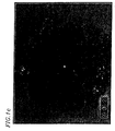
- FIG. 1a The gold-plated surface of the micro-electrode was observed with an optical microscope.
- the photomicrographs are shown in Figures 1a to 1c.
- Figures 1a, 1b, and 1c are microphotographs of the plated surfaces which were obtained at a current density of 1.0 A/dm 2 , 1.5 A/dm 2 , and 2.0 A/dm 2 , respectively.
- 1.0 A/dm 2 current density a substantially smooth plated surface was obtained.
- the porosity of the gold-plated surface was more significant and the area of the electrode surface was increased.
- Example 1 The micro-electrode surfaces obtained in Example 1 and slices of the mouse hippocampus (brain) were actually used to measure evoked potentials and noise levels.
- Hippocampus slices were obtained from a mouse. A five-week-old male c57black6 mouse was anesthetized with Fluothane and decapitated to remove a whole brain. The removed brain was immediately cooled in Ringer's solution on ice. A brain block containing only the hippocampus was dissected. Thereafter, the obtained brain block was cut by a tissue slicer to give a slice having a thickness of 250 ⁇ m. The slice was placed and tested on the micro-electrodes.
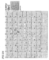
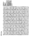
- FIG. 2a shows evoked potentials of cells on the gold-plated micro-electrode with respect to the above-described constant current stimuli.
- Figure 2a shows evoked potentials of the electrode obtained by electrolysis at a current density of 1.0 A/dm 2 .
- Figure 2c shows evoked potentials of the electrode obtained by electrolysis at a current density of 1.5 A/dm 2 .
- Figure 2e shows evoked potentials of the electrode obtained by electrolysis at a current density of 2.0 A/dm 2 .
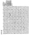
- Figures 2b, 2d and 2f show noise levels occurred in the respective gold-plated micro-electrodes shown in Figures 2a, 2c and 2e.
- the electrodes having the porous gold plating obtained by a higher level of current density had clear responses to the applied stimulus signals and it is possible to apply a constant current stimulus to the electrodes in an effective manner, as compared to the gold plating ( Figure 2a ) obtained by electrolysis at a current density of 1.0 A/dm 2 ( Figures 2c and 2e ).
- the micro-electrode having plating obtained at a current density of 1.5 A/dm 2 had a low impedance value and a satisfactory surface state.
- the plating ( Figure 2f ) obtained at a current density of 2.0 A/dm 2 had the lowest value
- the plating ( Figure 2b ) obtained at a current density of 1.0 A/dm 2 had a significant level of noise, and it was difficult to measure changes in potential of neurons with high precision.
- a micro-electrode surface area was measured or calculated by the following methods.
- the surface area of the micro-electrode having a porous gold-plated surface obtained in Example 1 at a current density of 1.5 A/dm 2 was measured with a gas adsorption method using CO gas.
- a gas adsorption method using CO gas As a specimen to be measured, 64 gold-plated micro-electrodes provided on a 1.3 mm ⁇ 1.3 mm ⁇ 1.1 mm glass substrate (hereinafter referred to as a gold-plated micro-electrode block) were used.
- a single micro-electrode is too small to be used as a specimen to be measured with the gas adsorption method.
- platinum black-plated micro-electrode block 64 platinum black-plated micro-electrodes (hereinafter referred to as a platinum black-plated micro-electrode block) provided on a glass substrate as described above but having platinum black plating by a conventional method (electrolytic plating) instead of gold plating, were used as comparative specimens. Note that each of the specimen blocks had a weight of 0.004 g. The results of the measurement are shown in Table 2. Results of Measurement of Surface Area of Electrode having Gold-plated Surface Specimen Surface area Gold-plated micro-electrode block 0.02 m 2 /g or less Platinum black-plated micro-electrode block (comparative example) 20.2 m 2 /g
- the value of S is the surface area of a 1.3 mm ⁇ 1.3 mm ⁇ 1.1 mm rectangular parallelepiped, i.e., 7.41 mm 2 .
- the value of s (projection area) is the surface area of the 64 electrodes each having a size of 50 ⁇ m ⁇ 50 ⁇ m, i.e., 0.16 mm 2 . Therefore, according to the measurement result of S' shown in Table 2, the value of ⁇ of the platinum black-plated micro-electrode is calculated to be 504955. Note that the value of ⁇ (an increase in the surface area) of the gold-plated electrode is below the detection limit of the gas adsorption method, and is estimated to be less than 455.
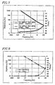
- the impedance of the micro-electrode of Example 1 having a porous gold-plated surface obtained at a current density of 1.5 A/dm 2 was measured by continuously changing frequency from 1 Hz to 100 kHz. In this measurement, a 0.3 mm ⁇ platinum line was used as a counter electrode and the measurement was conducted in 1.4 wt% NaCl aqueous solution. The bias voltage was zero volts, and the amplitude of a measuring voltage was 50 mV. The results are shown in Figure 3 .
- Figure 3 is a Bode diagram, well-known to those skilled in the art, showing the results of the impedance measurement, where the logarithm of the absolute value of a measured impedance Z (i.e., log
- the measurement system is represented by an equivalent circuit, thereby quantifying the surface area of the micro-electrode.
- the measurement system including the micro-electrode can be estimated to be equivalent to a circuit actually including a capacitance generated between the ITO circuit pattern portion and a solution, a resistance generated on a micro-electrode interface, and the like, in addition to the resistance of the solution, the resistance of the ITO circuit pattern, a capacitance of an,electric double layer in the micro-electrode surface, and the like, which are complicatedly connected in series and parallel.
- Figure 4a shows an equivalent circuit of the measurement system including micro-electrode.
- R 1 represents the resistance of the ITO circuit pattern portion (which does not contact the solution)
- R 2 represents the resistance of the ITO circuit pattern portion and the resistance of the solution
- R 3 represents the resistance of the micro
- the equivalent circuit shown in Figure 4a was simulated by calculating the synthetic impedance of the equivalent circuit by changing R 1 , R 2 , C 1 and C 2 to select a combination of R 1 , R 2 , R 3 , C 1 and C 2 which provide a Bode diagram most approximate to the Bode diagram shown in Figure 3.
- of the above-described synthetic impedance and the phase ⁇ are represented by
- Figure 7 is a graph showing the actually measured values of the impedance of a micro-electrode used as a control, which does not have a gold-plated surface.
- the measurement conditions are the same as used in measuring the impedance of the multiple electrode having the above-described gold-plated surface ( Figure 3 ).
- the capacitance of the electric double layer of a micro-electrode having a gold-plated surface is represented by C A and the capacitance of the electric double layer of the micro-electrode before gold plating treatment is represented by C B .
- the value of electrostatic capacity C ap is proportional to the surface area of the electrode. Therefore, the above-described relationship indicates that the surface area of a micro-electrode having a gold-plated surface is increased by a factor of 40 by the provision of the gold plating.
- Figure 9 is a graph showing the actually measured values of the impedance of a micro-electrode having a platinum black-plated surface in a manner similar to a micro-electrode having a gold-plated surface.
- the measurement conditions are the same as used in measuring the impedance of a micro-electrode having a gold-plated surface ( Figure 3 ).
- the capacitance of the electric double layer of a micro-electrode having a gold-plated surface is represented by C A and the capacitance of the electric double layer of the micro-electrode before gold plating treatment is represented by C B .
- the surface area needs to be increased by a factor of 10 or more using gold plating, compared to the projection area.
- a planar multiple electrode having porous gold plating obtained by electrolysis at a current density of 1. 5 A/dm 2 was subjected to a lifetime test in comparison with a conventional electrode (platinum black plating).
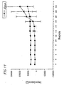
- a lifetime test an experiment similar to a typical acute experiment was repeated. Specifically, an experiment as described in Example 2 was repeated. After the end of each experiment, the electrode was treated with collagenase (20 u/ml) overnight and a cell slice specimen was peeled off, followed by washing with distilled water. Subsequently, the impedance of the micro-electrode was measured.
- Figure 11 is a graph in which the impedance changes after the end of each experiment are plotted. According to the result, an increase and variation in the impedance with an increase in the number of times of use is smaller than that of conventional plating (platinum black plating).
- a multiple electrode for extracellular recording which has a high strength, is capable of recording the electrical activities of neurons for a long period of time, and is easy to recycle.
- a plurality of micro-electrodes included in the multiple electrode have a low level of impedance without loss of the strength by utilizing porous gold plating. Therefore, it is easy to apply a constant current stimulus to the multiple electrode, and the multiple electrode is preferably suited to monitor a response of a cultured cell to an electrical stimulus.
Landscapes
- Health & Medical Sciences (AREA)
- Engineering & Computer Science (AREA)
- Life Sciences & Earth Sciences (AREA)
- Biomedical Technology (AREA)
- Physics & Mathematics (AREA)
- Chemical & Material Sciences (AREA)
- General Health & Medical Sciences (AREA)
- Medicinal Chemistry (AREA)
- General Physics & Mathematics (AREA)
- Urology & Nephrology (AREA)
- Hematology (AREA)
- Food Science & Technology (AREA)
- Biophysics (AREA)
- Analytical Chemistry (AREA)
- Biochemistry (AREA)
- Optics & Photonics (AREA)
- Molecular Biology (AREA)
- Immunology (AREA)
- Pathology (AREA)
- Nuclear Medicine, Radiotherapy & Molecular Imaging (AREA)
- Radiology & Medical Imaging (AREA)
- Animal Behavior & Ethology (AREA)
- Public Health (AREA)
- Veterinary Medicine (AREA)
- Investigating Or Analyzing Materials By The Use Of Electric Means (AREA)
- Measuring Or Testing Involving Enzymes Or Micro-Organisms (AREA)
Abstract
Description
| Current Density and Average Impedance | |
| Current density (A/dm2) | Average impedance (kΩ) |
| 1.0 | 336.39 ± 78.59 |
| 1.5 | 22.07 ± 1.95 |
| 2.0 | 16.56 ± 2.34 |
| Results of Measurement of Surface Area of Electrode having Gold-plated Surface | |
| Specimen | Surface area |
| Gold-plated micro-electrode block | 0.02 m2/g or less |
| Platinum black-plated micro-electrode block (comparative example) | 20.2 m2/g |

Claims (9)
- A multiple electrode for measuring electro-physiological characteristics of a cell, the electrode comprising:wherein the micro-electrodes have a porous conductive material on a surface thereof, the conductive material is selected from the group consisting of gold, titanium nitride, silver oxide, and tungsten, and the impedance of each of the micro-electrode is 50 kΩ or less.a plurality of micro-electrodes provided on a substrate; and a wiring portion for providing an electrical signal to the micro-electrodes or extracting an electrical signal from the micro-electrodes,
- A multiple electrode according to claim 1, wherein the porous conductive material is gold, and is provided by passage of current at a current density of 1.0 to 5.0 A/dm2 for 10 to 360 sec.
- A multiple electrode for measuring electro-physiological characteristics of a cell, the electrode comprising:wherein the surface area of the micro-electrode calculated from an electrostatic capacity of an equivalent circuit having substantially the same impedance as that of the micro-electrode, is greater than or equal to at least 10 times and less than 200 times the projection area of the micro-electrode, and the impedance of each of the micro-electrode is 50 kΩ or less.a plurality of micro-electrodes provided on a substrate; and a wiring portion for providing an electrical signal to the micro-electrodes or extracting an electrical signal from the micro-electrodes,
- A multiple electrode according to claim 3, wherein a surface area of the micro-electrode measured by a gas adsorption method is less than or equal to 5 × 10⁵ times the projection area of the micro-electrode.
- A multiple electrode according to any of claims 1 to 4, wherein the micro-electrodes are arranged on the substrate in a form of a matrix, the wiring portion includes a lead line connected to the micro-electrode and an electrical junction connected to an end of the lead line, and at least a surface of the lead line is covered with an insulating layer.
- A multiple electrode according to any of claims 1, 3, 4 and 5, wherein the porous conductive material is provided by etching.
- An integrated cell installer comprising a multiple electrode according to any of claims 1 to 6, wherein the integrated cell installer has a cell installing region for placing a cell or tissue on the substrate of the multiple electrode.
- A cellular potential measuring apparatus comprising: an integrated cell installer according to claim 7; an output signal processor connected to the micro-electrodes for processing an output signal due to an electro-physiological acitivity of a cell or tissue; and a stimulus signal provider for optionally providing an electrical stimulus to the cell or tissue.
- A cellular potential measuring system comprising: a cellular potential measuring apparatus according to claim 8; an optical monitoring apparatus for optically monitoring a cell or tissue; and/or a cell culture apparatus for controlling the culture environment of the cell or tissue.
Applications Claiming Priority (1)
| Application Number | Priority Date | Filing Date | Title |
|---|---|---|---|
| PCT/JP2001/005289 WO2003001194A1 (en) | 2001-06-20 | 2001-06-20 | Extracellular recording electrode |
Publications (2)
| Publication Number | Publication Date |
|---|---|
| EP1398625A1 true EP1398625A1 (en) | 2004-03-17 |
| EP1398625A4 EP1398625A4 (en) | 2005-03-30 |
Family
ID=11737463
Family Applications (1)
| Application Number | Title | Priority Date | Filing Date |
|---|---|---|---|
| EP01941137A Withdrawn EP1398625A4 (en) | 2001-06-20 | 2001-06-20 | EXTRACELLULAR RECORDING ELECTRODE |
Country Status (4)
| Country | Link |
|---|---|
| US (1) | US7041492B2 (en) |
| EP (1) | EP1398625A4 (en) |
| CN (1) | CN1204396C (en) |
| WO (1) | WO2003001194A1 (en) |
Families Citing this family (8)
| Publication number | Priority date | Publication date | Assignee | Title |
|---|---|---|---|---|
| US7136696B2 (en) | 2002-04-05 | 2006-11-14 | The Cleveland Clinic Foundation | Neuron signal analysis system and method |
| US20050256541A1 (en) * | 2004-04-30 | 2005-11-17 | Medtronic, Inc. | Catheter with temporary stimulation electrode |
| US7504069B2 (en) * | 2004-06-21 | 2009-03-17 | Wisconsin Alumni Research Foundation | Micro device for high resolution delivery and monitoring of stimuli to a biological object, in vitro |
| CN101246141B (en) * | 2008-02-26 | 2012-03-14 | 南京大学 | Electro-chemistry detecting method for fast identifying peripheral nerve bundle nature |
| BRPI1011317B8 (en) | 2009-06-09 | 2021-12-21 | Neuronano Ab | Medical microelectrode for soft tissue insertion, medical microelectrode beam and arrangement thereof |
| AU2011294993B2 (en) | 2010-08-25 | 2014-05-01 | Neuronano Ab | Displacement resistant microelectrode, microelectrode bundle and microelectrode array |
| US20170122928A1 (en) * | 2013-05-05 | 2017-05-04 | The Trustees Of Boston College | Coaxial electrode arrays and methods thereof |
| EP3724655B1 (en) | 2017-12-13 | 2023-08-30 | Fondazione Istituto Italiano di Tecnologia | Method and device for recording intracellular action potentials in electrogenic cells |
Family Cites Families (11)
| Publication number | Priority date | Publication date | Assignee | Title |
|---|---|---|---|---|
| US5143090A (en) * | 1989-11-02 | 1992-09-01 | Possis Medical, Inc. | Cardiac lead |
| US5282844A (en) * | 1990-06-15 | 1994-02-01 | Medtronic, Inc. | High impedance, low polarization, low threshold miniature steriod eluting pacing lead electrodes |
| JP2949845B2 (en) * | 1990-11-30 | 1999-09-20 | 松下電器産業株式会社 | Electrodes for measuring cell electrical activity |
| JP3101122B2 (en) | 1993-04-16 | 2000-10-23 | 松下電器産業株式会社 | Integrated composite electrode |
| JP3193471B2 (en) | 1992-09-04 | 2001-07-30 | 松下電器産業株式会社 | Integrated composite electrode |
| DE69333945T2 (en) * | 1992-09-04 | 2006-06-29 | Matsushita Electric Industrial Co., Ltd., Kadoma | Flat electrode |
| US5810725A (en) * | 1993-04-16 | 1998-09-22 | Matsushita Electric Industrial Co., Ltd. | Planar electrode |
| US5563067A (en) | 1994-06-13 | 1996-10-08 | Matsushita Electric Industrial Co., Ltd. | Cell potential measurement apparatus having a plurality of microelectrodes |
| US5662697A (en) | 1995-10-17 | 1997-09-02 | Pacesetter, Inc. | Transvenous internal cardiac defibrillation apparatus having lead and electrode providing even distribution of electrical charge |
| JPH11187865A (en) | 1997-12-25 | 1999-07-13 | Matsushita Electric Ind Co Ltd | Cell potential measuring electrode and measuring device using the same |
| JP4017058B2 (en) * | 1999-05-31 | 2007-12-05 | 誠 石田 | Probe and sensor equipped with the same |
-
2001
- 2001-06-20 EP EP01941137A patent/EP1398625A4/en not_active Withdrawn
- 2001-06-20 CN CN01812189.6A patent/CN1204396C/en not_active Expired - Fee Related
- 2001-06-20 WO PCT/JP2001/005289 patent/WO2003001194A1/en not_active Ceased
- 2001-06-20 US US10/048,662 patent/US7041492B2/en not_active Expired - Lifetime
Also Published As
| Publication number | Publication date |
|---|---|
| US20030111343A1 (en) | 2003-06-19 |
| CN1440505A (en) | 2003-09-03 |
| US7041492B2 (en) | 2006-05-09 |
| WO2003001194A1 (en) | 2003-01-03 |
| CN1204396C (en) | 2005-06-01 |
| EP1398625A4 (en) | 2005-03-30 |
Similar Documents
| Publication | Publication Date | Title |
|---|---|---|
| EP1300678B1 (en) | Extracellular recording integrated composite electrode | |
| US5810725A (en) | Planar electrode | |
| Franks et al. | Impedance characterization and modeling of electrodes for biomedical applications | |
| JPWO2002055653A1 (en) | Extracellular potential measuring device, extracellular potential measuring method using the same, and high-speed drug screening apparatus equipped with the same | |
| EP1277054B1 (en) | Electrochemical sensing | |
| JP3570715B2 (en) | Signal detection sensor with multiple electrodes | |
| Huang et al. | Impedance based biosensor array for monitoring mammalian cell behavior | |
| US7041492B2 (en) | Extracellular recording electrode | |
| KR100564683B1 (en) | Method and apparatus for detecting physicochemical changes emitted by cell | |
| WO1996010742A1 (en) | Electrochemical assessment of cell behaviour and metabolic activity | |
| JP3624292B2 (en) | Biological sample activity signal measuring apparatus and measuring method | |
| TW524973B (en) | Extracellular recording electrode | |
| EP3210014B1 (en) | A device comprising a multi electrode array (mea) | |
| Demarest et al. | Segregation of gastric Na and Cl transport: a vibrating probe and microelectrode study | |
| KR100481743B1 (en) | Extracellular recording electrode | |
| Hung et al. | Micromachined electrodes for retinal prostheses | |
| JP2004020238A (en) | Biological reaction measuring chip, and biological reaction measuring method and apparatus using the same | |
| Narayanan et al. | Method to quantify the effect of passivation layer in bio-impedance sensors |
Legal Events
| Date | Code | Title | Description |
|---|---|---|---|
| PUAI | Public reference made under article 153(3) epc to a published international application that has entered the european phase |
Free format text: ORIGINAL CODE: 0009012 |
|
| 17P | Request for examination filed |
Effective date: 20021206 |
|
| AK | Designated contracting states |
Kind code of ref document: A1 Designated state(s): AT BE CH CY DE DK ES FI FR GB GR IE IT LI LU MC NL PT SE TR |
|
| A4 | Supplementary search report drawn up and despatched |
Effective date: 20050215 |
|
| RIC1 | Information provided on ipc code assigned before grant |
Ipc: 7A 61N 1/05 B Ipc: 7G 01N 27/416 B Ipc: 7G 01N 27/30 A |
|
| 17Q | First examination report despatched |
Effective date: 20060919 |
|
| STAA | Information on the status of an ep patent application or granted ep patent |
Free format text: STATUS: THE APPLICATION HAS BEEN WITHDRAWN |
|
| 18W | Application withdrawn |
Effective date: 20070214 |