EP1397022A1 - Microphone devices - Google Patents
Microphone devices Download PDFInfo
- Publication number
- EP1397022A1 EP1397022A1 EP03005522A EP03005522A EP1397022A1 EP 1397022 A1 EP1397022 A1 EP 1397022A1 EP 03005522 A EP03005522 A EP 03005522A EP 03005522 A EP03005522 A EP 03005522A EP 1397022 A1 EP1397022 A1 EP 1397022A1
- Authority
- EP
- European Patent Office
- Prior art keywords
- fet
- output
- microphone
- electrode
- arrangement
- Prior art date
- Legal status (The legal status is an assumption and is not a legal conclusion. Google has not performed a legal analysis and makes no representation as to the accuracy of the status listed.)
- Withdrawn
Links
Images

Classifications
-
- H—ELECTRICITY
- H04—ELECTRIC COMMUNICATION TECHNIQUE
- H04R—LOUDSPEAKERS, MICROPHONES, GRAMOPHONE PICK-UPS OR LIKE ACOUSTIC ELECTROMECHANICAL TRANSDUCERS; ELECTRIC HEARING AIDS; PUBLIC ADDRESS SYSTEMS
- H04R19/00—Electrostatic transducers
- H04R19/01—Electrostatic transducers characterised by the use of electrets
- H04R19/016—Electrostatic transducers characterised by the use of electrets for microphones
Definitions
- the present invention is generically directed on microphone devices sized for hearing device implementation, microphone arrangements sized for hearing device implementation as well as to a method for biasing a FET buffer output stage of a microphone device.
- the present invention departs from problems which have been recognized in context with capacitive microphones, whereat a capacitive element provides for acoustical/electrical conversion.
- a capacitive element which performs conversion of mechanical movement of at least one of the capacitor plates into a respective electric signal necessitates a buffer stage to tap off the resulting electric signal, which buffer must only consume very little input current. Therefore, it is customary to provide such a buffer stage with at least one FET.
- such a buffer stage will be used wherever in such microphone device the acoustical/electrical converting element may not be loaded by a relatively heavy current.
- a known microphone device 4 is schematically shown. It comprises a mechanical/electrical conversion element 1, which may customarily be realized by a capacitance element with a mechanically moveable or swingable capacitance plate as mentioned above.
- the electric output signal of such conversion unit 1 is fed to a buffer stage 3, namely on one hand to the gate of a Mos-FET 5 a and on the other hand to reference potential line 7 a connected to the source electrode S of the Mos-FET 5 a .
- the drain electrode D of the Mos-FET 5 a is on one hand operationally connected via a resistance element R S to a biasing input tap V biasa and on the other hand to the signal output of the device, A 3a .
- the Bulk of the Mos-FET is denoted with B in Fig. 1.
- the gate electrode G of the Mos-FET 5 a is operationally connected either via a resistance element R G or via another device acting as resistive element to the reference potential line 7 a .
- the mechanical/electrical conversion unit 1 has an output which on one hand is operationally connected to the gate electrode G of a JFET element 5 b , the drain electrode D thereof is operationally connected to a bias tap V biasb of the device 4.
- the source electrode S of the JFET 5 b is connected to an output tap A 3b of the device 4 and connected via a resistance element R S to the reference potential line 7 b .
- the gate G of the JFET 5 b is operationally connected to the reference potential line 7 b by a resistance element R G .
- the bias tap V biasa according to fig. 1 or V biasb according to fig. 2 is connected to respective voltage sources, as biasing voltage sources, 9a or 9b respectively.
- the respective outputs A 3a and A 3b are operationally connected via a coupling capacitor C a , C b respectively to respective preamplifiers 11 a and 11 b .
- the bias voltage sources 9 a,b as well as coupling capacitors C and preamplifiers 11 are thereby customarily mounted on a circuit board, or integrated on an integrated circuit, separate from the microphone 4 with the buffer stage 3 having the respective output FET 5a and 5b with the additional resistance elements.
- V biasa and V biasb must be extremely clean, i.e. on one hand clean of noise and on the other hand very stable. Therefore, very high requirements have to be fulfilled with respect to noise level reduction as well as with respect to stabilizing the applied voltage with respect to variations of power supply voltage. E.g. for the power supply rejection ratio PSRR 60 to 80 dB rejection is required customarily.
- Disturbances of the biasing voltage are transmitted without significant attenuation to the output of the microphone device, i.e. A 3a , A 3b .
- an output loudspeaker of a hearing device will cause modulation of the power supply, i.e. the battery voltage, which modulation will be perceivable in the electric audio signal if the voltage applied to V biasa,b provides for a too low PSSR.
- biasing comprises applying a substantially constant voltage-independent current.
- the voltage-independent current is preferably applied to the drain electrode of the Mos-FET.
- the voltage-independent current is preferably applied to the source electrode of the JFET.
- a microphone device which comprises a buffer stage with an output FET.
- the device has exclusively a reference potential tap and an output signal tap. Having only two taps such microphone device e.g. significantly reduces the efforts to be electrically connected to the downstream network and thereby e.g. the known problems of establishing clean, optimally conductive connections by automation.
- this microphone device with only two output taps is especially preferably realized with the output FET being a Mos-FET.
- the output FET being a Mos-FET.
- such device has a capacitance as an acoustical/electrical converter element.
- a microphone device again sized for hearing device implementation, which comprises a buffer stage with an output FET and wherein the device comprises an output signal tap from an electrode of the output FET, which output is not shunted, e.g. by a resistance, to a further tap of the device.
- the output FET as a JFET there is thereby reduced the number of electronic elements within the device at least by one resistance, which is normally provided between the source electrode output and reference potential line.
- this microphone device too comprises a capacitance as an acoustical/electrical converter element.
- a microphone arrangement sized for hearing device implementation which comprises an output buffer stage of a microphone unit, which stage having an output FET, one electrode thereof being operationally connected to the input of a preamplifier and wherein there is present a current source operationally connected to the said electrode of the output FET.
- the FET is a Mos-FET and the electrode is the drain electrode.
- the FET is a JFET
- the said electrode is the source electrode.
- the current source is preferably operationally connected between the source electrode and a reference potential of the arrangement.
- the source electrode is not additionally connected by a resistive branch to the reference potential line.
- the current source is preferably operationally connected to the drain electrode, which is preferably not operationally connected to any further biasing source.
- the present invention is further directed on a hearing device which comprises at least one microphone device as outlined above or which comprises at least one microphone arrangement as discussed above.
- a constant current source 15 a is applied to the drain electrode of Mos-FET 5 a and via coupling capacitor Ca, is operationally connected to the preamplifier 11a.
- the current source 15a may thereby possibly be implemented within the microphone device 4 or, as shown in fig. 3, within the circuitry downstream of such device 4.
- the biasing input V biasa as of fig. 1 becomes obsolete and is thereby preferably completely omitted from the device 4, altogether with resistance R S according to fig. 1.
- a microphone device which has only two taps, namely one A 3a for the output signal and possibly for the biasing current I and one for applying reference potential to the circuitry.
- fig. 4 those elements which have already been described in context with fig. 2 need not to be described once again and are referred to with the same reference numbers.
- fig. 4 there is provided a constant current sink-source 15b between the source electrode S of the JFET 5b and the reference potential line 7 b .
- the source resistance element R S according to fig. 2 is removed so that the source electrode S of JFET 5 b is not connected or shunted by such resistance element to the reference potential line 7 b .
- biasing at least comprises providing such biasing by means of a constant current or constant current source
- the output signal of the microphone device as at A 3 becomes much less sensitive to supply voltage variation, because PSSR to the respective current sources 15 is much easier realized than to the customarily applied voltage sources.
- provision of the constant current source 15 b significantly reduces PSSR problems.
- microphone devices are thereby realized with fewer electronic elements and additionally even with fewer taps. This significantly facilitates manufacturing and assembling of respective hearing devices with such microphone devices or arrangements.
Landscapes
- Physics & Mathematics (AREA)
- Engineering & Computer Science (AREA)
- Acoustics & Sound (AREA)
- Signal Processing (AREA)
- Circuit For Audible Band Transducer (AREA)
- Electrostatic, Electromagnetic, Magneto- Strictive, And Variable-Resistance Transducers (AREA)
Abstract
Description
- The present invention is generically directed on microphone devices sized for hearing device implementation, microphone arrangements sized for hearing device implementation as well as to a method for biasing a FET buffer output stage of a microphone device.
- Thereby, the present invention departs from problems which have been recognized in context with capacitive microphones, whereat a capacitive element provides for acoustical/electrical conversion. Such capacitive element which performs conversion of mechanical movement of at least one of the capacitor plates into a respective electric signal necessitates a buffer stage to tap off the resulting electric signal, which buffer must only consume very little input current. Therefore, it is customary to provide such a buffer stage with at least one FET.
- More generalizing, such a buffer stage will be used wherever in such microphone device the acoustical/electrical converting element may not be loaded by a relatively heavy current.
- It is further customary to integrate the buffer stage together with the acoustical/electrical conversion element into one unitary microphone device.
- In fig. 1 a known
microphone device 4 is schematically shown. It comprises a mechanical/electrical conversion element 1, which may customarily be realized by a capacitance element with a mechanically moveable or swingable capacitance plate as mentioned above. The electric output signal ofsuch conversion unit 1 is fed to abuffer stage 3, namely on one hand to the gate of a Mos-FET 5a and on the other hand to reference potential line 7a connected to the source electrode S of the Mos-FET 5a. The drain electrode D of the Mos-FET 5a is on one hand operationally connected via a resistance element RS to a biasing input tap Vbiasa and on the other hand to the signal output of the device, A3a. The Bulk of the Mos-FET is denoted with B in Fig. 1. The gate electrode G of the Mos-FET 5a is operationally connected either via a resistance element RG or via another device acting as resistive element to the reference potential line 7a. - According to fig. 2 in a further known
device 4 the mechanical/electrical conversion unit 1 has an output which on one hand is operationally connected to the gate electrode G of a JFET element 5b, the drain electrode D thereof is operationally connected to a bias tap Vbiasb of thedevice 4. The source electrode S of the JFET 5b is connected to an output tap A3b of thedevice 4 and connected via a resistance element RS to the reference potential line 7b. The gate G of the JFET 5b is operationally connected to the reference potential line 7b by a resistance element RG. - Customarily the bias tap Vbiasa according to fig. 1 or Vbiasb according to fig. 2 is connected to respective voltage sources, as biasing voltage sources, 9a or 9b respectively. The respective outputs A3a and A3b are operationally connected via a coupling capacitor Ca, Cb respectively to respective preamplifiers 11a and 11b. The bias voltage sources 9a,b as well as coupling capacitors C and preamplifiers 11 are thereby customarily mounted on a circuit board, or integrated on an integrated circuit, separate from the
microphone 4 with thebuffer stage 3 having therespective output FET 5a and 5b with the additional resistance elements. -
- We understand under a voltage source a source which delivers a voltage substantially independent of the output current.
- We understand as a current source a source which delivers a constant current substantially independent of the output voltage.
- The voltage applied to the respective biasing inputs Vbiasa and Vbiasb must be extremely clean, i.e. on one hand clean of noise and on the other hand very stable. Therefore, very high requirements have to be fulfilled with respect to noise level reduction as well as with respect to stabilizing the applied voltage with respect to variations of power supply voltage. E.g. for the power supply rejection ratio PSRR 60 to 80 dB rejection is required customarily.
- Disturbances of the biasing voltage are transmitted without significant attenuation to the output of the microphone device, i.e. A3a, A3b. In practice especially an output loudspeaker of a hearing device will cause modulation of the power supply, i.e. the battery voltage, which modulation will be perceivable in the electric audio signal if the voltage applied to Vbiasa,b provides for a too low PSSR.
- For attempting low power appliances the very high requirements to the PSRR is a serious problem. It would clearly be a need to exploit newer up-to-date IC technologies with low threshold voltages by operating the overall analog network of a hearing device without DC/DC converter electrically supplied directly from a power supply battery. Thereby, one would gain different advantages, namely
- 1. with respect to efficiency
- 2. with respect to less external components (no DC/DC converter)
- 3. with respect to power consumption. E.g. an analog to digital converter consuming 150 µA current consumes considerably more power from a 1.8 V power supply than from a 1.3 V supply.
-
- One serious problem to be resolves when attempts are made to operate the analog circuitry as applied to a hearing device directly from the power supply, namely a battery or an accumulator battery, is that a high PSRR with respect to the voltage applied to Vbias is only very difficult to realize.
- This problem is especially pronounced if the solution thereof should not imply the use of additional electronic components.
- It is an object of the present invention to solve this problem. This is realized by a method for biasing a FET output buffer stage of a microphone device sized for hearing device implementation, wherein biasing comprises applying a substantially constant voltage-independent current. Thereby, it has been recognized and exploited that the influence of power supply voltage variation may be significantly easier attenuated with respect to the current of a current source than this is possible with respect to the voltage of a voltage source.
- In a preferred embodiment wherein the output stage comprises a Mos-FET output stage the voltage-independent current is preferably applied to the drain electrode of the Mos-FET. In the case where the output stage comprises an output JFET, the voltage-independent current is preferably applied to the source electrode of the JFET.
- Realization of this method according to the present invention, namely of biasing a FET output buffer stage of such a device further significantly simplifies construction of such device:
- There is realized a microphone device according to the present invention, which comprises a buffer stage with an output FET. The device has exclusively a reference potential tap and an output signal tap. Having only two taps such microphone device e.g. significantly reduces the efforts to be electrically connected to the downstream network and thereby e.g. the known problems of establishing clean, optimally conductive connections by automation.
- Thereby this microphone device with only two output taps is especially preferably realized with the output FET being a Mos-FET. In a preferred mode such device has a capacitance as an acoustical/electrical converter element.
- On the other hand by the concept according to the present invention it is possible to realize according to the present invention a microphone device, again sized for hearing device implementation, which comprises a buffer stage with an output FET and wherein the device comprises an output signal tap from an electrode of the output FET, which output is not shunted, e.g. by a resistance, to a further tap of the device. Especially when providing the output FET as a JFET there is thereby reduced the number of electronic elements within the device at least by one resistance, which is normally provided between the source electrode output and reference potential line.
- Again in a preferred embodiment this microphone device too comprises a capacitance as an acoustical/electrical converter element.
- According to the present invention there is further provided a microphone arrangement sized for hearing device implementation, which comprises an output buffer stage of a microphone unit, which stage having an output FET, one electrode thereof being operationally connected to the input of a preamplifier and wherein there is present a current source operationally connected to the said electrode of the output FET. In a first most preferred embodiment the FET is a Mos-FET and the electrode is the drain electrode.
- In a further preferred embodiment of this arrangement the FET is a JFET, and the said electrode is the source electrode. Thereby, still applying a JFET, the current source is preferably operationally connected between the source electrode and a reference potential of the arrangement. Thereby further preferred, the source electrode is not additionally connected by a resistive branch to the reference potential line.
- On the other hand, looking back on the first preferred embodiment, wherein the FET is a Mos-FET, then the current source is preferably operationally connected to the drain electrode, which is preferably not operationally connected to any further biasing source.
- The present invention is further directed on a hearing device which comprises at least one microphone device as outlined above or which comprises at least one microphone arrangement as discussed above.
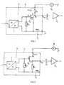
- The invention shall now be exemplified with the help of figures.
- These figures show:
- Fig. 3
- a microphone device as a part of a microphone arrangement according to the present invention and performing the method according to the present invention, shown as an inventive improvement over a prior art embodiment as shown in fig. 1;
- Fig. 4
- a further preferred embodiment of a device, part of an arrangement and operating the method according to the present invention and shown as an improvement over the prior art embodiment as shown in fig. 2.
- In fig. 3 as departing from a known prior art embodiment as of fig. 1, the same elements which have already been described in context with fig. 1 are not described anymore and are referred to with the same reference numbers. According to this embodiment of the present invention a constant current source 15a is applied to the drain electrode of Mos-FET 5a and via coupling capacitor Ca, is operationally connected to the
preamplifier 11a. Thecurrent source 15a may thereby possibly be implemented within themicrophone device 4 or, as shown in fig. 3, within the circuitry downstream ofsuch device 4. Thereby the biasing input Vbiasa as of fig. 1 becomes obsolete and is thereby preferably completely omitted from thedevice 4, altogether with resistance RS according to fig. 1. There is thereby provided a microphone device which has only two taps, namely one A3a for the output signal and possibly for the biasing current I and one for applying reference potential to the circuitry. - In fig. 4 those elements which have already been described in context with fig. 2 need not to be described once again and are referred to with the same reference numbers. According to fig. 4 there is provided a constant current sink-
source 15b between the source electrode S of the JFET 5b and the reference potential line 7b. Thereby the source resistance element RS according to fig. 2 is removed so that the source electrode S of JFET 5b is not connected or shunted by such resistance element to the reference potential line 7b. - Due to the fact that according to the present invention biasing at least comprises providing such biasing by means of a constant current or constant current source, the output signal of the microphone device as at A3 becomes much less sensitive to supply voltage variation, because PSSR to the respective current sources 15 is much easier realized than to the customarily applied voltage sources. Even in the embodiment according to fig. 4 where the JFET still needs a biasing voltage to the gate electrode G, provision of the constant current source 15b significantly reduces PSSR problems. Additionally according to the invention, microphone devices are thereby realized with fewer electronic elements and additionally even with fewer taps. This significantly facilitates manufacturing and assembling of respective hearing devices with such microphone devices or arrangements.
Claims (18)
- A microphone device sized for a hearing device implementation comprising a buffer stage with an output FET, said device having exclusively a reference potential tap and an output signal tap.
- The device of claim 1, wherein said output FET is a Mos-FET.
- The device of claim 1 having a capacitance as an acoustical/electrical converter element.
- A microphone device sized for hearing device implementation, comprising a buffer stage with an output FET, said device comprising an output signal tap from an electrode of said output FET, said output not having a dc path via another built-in component to a further tap of said device.
- The device of claim 4, wherein said FET is a JFET.
- The device of claim 4 having a capacitance as acoustical/electrical converter element.
- A microphone arrangement sized for hearing device implementation, comprising an output buffer stage of a microphone stage with an output FET, one electrode thereof being operationally connected to the input of a preamplifier, a current source operationally connected to said input and said output.
- The arrangement of claim 7, wherein said FET is a Mos-FET and said electrode is the drain electrode.
- The arrangement of claim 7, wherein said FET is a JFET and said electrode is a source electrode.
- The arrangement of claim 9, wherein said current source is operationally connected between said source electrode and a reference potential line of said arrangement.
- The arrangement of claim 10, wherein said drain electrode is not connected by a resistive branch to said ground potential line.
- The arrangement of claim 7, wherein said FET is a Mos-FET, said current source is operationally connected to the drain electrode and said drain electrode not being operationally connected to a further biasing source.
- The arrangement of claim 12, wherein said current source is operationally connected to said drain electrode.
- A method for biasing a FET output buffer stage of a microphone device sized for hearing device implementation, wherein said biasing comprises the step of applying a substantially constant supply-voltage-independent current.
- The method of claim 14, wherein said output stage comprises a Mos-FET output stage, further comprising the step of applying said current to the drain electrode of said Mos-FET.
- The method of claim 11, wherein said buffer output stage comprises an output JFET, further comprising the step of applying said constant current to the source electrode of said JFET.
- A hearing device comprising a microphone device according to one of the claims 1 to 6.
- A hearing device with at least one microphone arrangement according to one of the claims 7 to 13.
Priority Applications (2)
| Application Number | Priority Date | Filing Date | Title |
|---|---|---|---|
| US10/386,305 US20040179706A1 (en) | 2003-03-11 | 2003-03-11 | Microphone devices |
| EP03005522A EP1397022A1 (en) | 2003-03-11 | 2003-03-11 | Microphone devices |
Applications Claiming Priority (2)
| Application Number | Priority Date | Filing Date | Title |
|---|---|---|---|
| US10/386,305 US20040179706A1 (en) | 2003-03-11 | 2003-03-11 | Microphone devices |
| EP03005522A EP1397022A1 (en) | 2003-03-11 | 2003-03-11 | Microphone devices |
Publications (1)
| Publication Number | Publication Date |
|---|---|
| EP1397022A1 true EP1397022A1 (en) | 2004-03-10 |
Family
ID=33454316
Family Applications (1)
| Application Number | Title | Priority Date | Filing Date |
|---|---|---|---|
| EP03005522A Withdrawn EP1397022A1 (en) | 2003-03-11 | 2003-03-11 | Microphone devices |
Country Status (2)
| Country | Link |
|---|---|
| US (1) | US20040179706A1 (en) |
| EP (1) | EP1397022A1 (en) |
Families Citing this family (4)
| Publication number | Priority date | Publication date | Assignee | Title |
|---|---|---|---|---|
| WO2008041064A2 (en) * | 2006-10-06 | 2008-04-10 | Freescale Semiconductor, Inc. | Detection circuit for detecting the connection of an accessory to a mobile device and method thereof |
| WO2013077932A1 (en) | 2011-11-23 | 2013-05-30 | Ag Phonak | Cic hearing device |
| US10241750B1 (en) * | 2018-01-28 | 2019-03-26 | Columbia Network Security Inc. | Method and apparatus for disabling audio |
| CN112334867B (en) | 2018-05-24 | 2025-11-11 | 纽约州立大学研究基金会 | Capacitive sensor |
Citations (4)
| Publication number | Priority date | Publication date | Assignee | Title |
|---|---|---|---|---|
| US4539441A (en) * | 1981-09-03 | 1985-09-03 | Robert Bosch Gmbh | Hearing-aid with integrated circuit electronics |
| EP0664605A1 (en) * | 1994-01-21 | 1995-07-26 | Matsushita Electric Industrial Co., Ltd. | Amplifier device |
| US6160450A (en) * | 1999-04-09 | 2000-12-12 | National Semiconductor Corporation | Self-biased, phantom-powered and feedback-stabilized amplifier for electret microphone |
| US20020071578A1 (en) * | 2000-07-05 | 2002-06-13 | Van Der Zwan Eric Jurgen | A/D converter with integrated biasing for a microphone |
Family Cites Families (3)
| Publication number | Priority date | Publication date | Assignee | Title |
|---|---|---|---|---|
| CA1024239A (en) * | 1972-04-17 | 1978-01-10 | Rca Limited | Low noise detector amplifier |
| US4516428A (en) * | 1982-10-28 | 1985-05-14 | Pan Communications, Inc. | Acceleration vibration detector |
| US4993072A (en) * | 1989-02-24 | 1991-02-12 | Lectret S.A. | Shielded electret transducer and method of making the same |
-
2003
- 2003-03-11 EP EP03005522A patent/EP1397022A1/en not_active Withdrawn
- 2003-03-11 US US10/386,305 patent/US20040179706A1/en not_active Abandoned
Patent Citations (4)
| Publication number | Priority date | Publication date | Assignee | Title |
|---|---|---|---|---|
| US4539441A (en) * | 1981-09-03 | 1985-09-03 | Robert Bosch Gmbh | Hearing-aid with integrated circuit electronics |
| EP0664605A1 (en) * | 1994-01-21 | 1995-07-26 | Matsushita Electric Industrial Co., Ltd. | Amplifier device |
| US6160450A (en) * | 1999-04-09 | 2000-12-12 | National Semiconductor Corporation | Self-biased, phantom-powered and feedback-stabilized amplifier for electret microphone |
| US20020071578A1 (en) * | 2000-07-05 | 2002-06-13 | Van Der Zwan Eric Jurgen | A/D converter with integrated biasing for a microphone |
Also Published As
| Publication number | Publication date |
|---|---|
| US20040179706A1 (en) | 2004-09-16 |
Similar Documents
| Publication | Publication Date | Title |
|---|---|---|
| US7800443B2 (en) | Circuit arrangement for providing an analog signal, and electronic apparatus | |
| KR102772486B1 (en) | Class-d amplifier with multiple independent output stages | |
| US7498879B2 (en) | Summing comparator for higher order class D amplifiers | |
| EP1771943B1 (en) | Single supply direct drive amplifier | |
| US8288971B2 (en) | Integrated and programmable microphone bias generation | |
| TWI257036B (en) | Low dropout voltage regulator, integrated circuit, electronic device and method of compensating the low dropout voltage regulator | |
| US20090110213A1 (en) | Programmable integrated microphone interface circuit | |
| CN103138695A (en) | Audio amplification circuit | |
| WO1996027932A1 (en) | Power supply circuit and corresponding mounting configuration | |
| CN110248301B (en) | Sensing circuit and method of detecting electrical signals generated by a microphone | |
| US4539441A (en) | Hearing-aid with integrated circuit electronics | |
| US20040179706A1 (en) | Microphone devices | |
| US7688987B2 (en) | Electret microphone buffer circuit with significantly enhanced power supply rejection | |
| US20030179039A1 (en) | Amplifying circuit capable of limiting amplitude of output signal supplied to a speaker | |
| US11909387B2 (en) | Microphone with slew rate controlled buffer | |
| US6697612B2 (en) | Receiving section of a telephone | |
| US4644579A (en) | Shunt regulator for hands-free telephone | |
| KR100544014B1 (en) | Semiconductor Integrated Circuits Eliminate DC Offset Voltages | |
| JP2007189434A (en) | Semiconductor integrated circuit | |
| US6822510B1 (en) | Power-off, loop-through return-loss with negative capacitance | |
| US8416968B2 (en) | Audio device and audio input/output method | |
| CN223681102U (en) | Damping device | |
| KR102813905B1 (en) | Audio processing circuit | |
| JPH08317553A (en) | Multiple output power supply circuit | |
| CN116405830A (en) | Audio system |
Legal Events
| Date | Code | Title | Description |
|---|---|---|---|
| PUAI | Public reference made under article 153(3) epc to a published international application that has entered the european phase |
Free format text: ORIGINAL CODE: 0009012 |
|
| AK | Designated contracting states |
Kind code of ref document: A1 Designated state(s): AT BE BG CH CY CZ DE DK EE ES FI FR GB GR HU IE IT LI LU MC NL PT RO SE SI SK TR |
|
| AX | Request for extension of the european patent |
Extension state: AL LT LV MK RO |
|
| 17P | Request for examination filed |
Effective date: 20040212 |
|
| AKX | Designation fees paid |
Designated state(s): CH DE DK LI |
|
| 17Q | First examination report despatched |
Effective date: 20061229 |
|
| STAA | Information on the status of an ep patent application or granted ep patent |
Free format text: STATUS: THE APPLICATION IS DEEMED TO BE WITHDRAWN |
|
| 18D | Application deemed to be withdrawn |
Effective date: 20070709 |