EP1396934A1 - Compact balun with rejection filter for 802.11a and 802.11b simultaneous operation - Google Patents
Compact balun with rejection filter for 802.11a and 802.11b simultaneous operation Download PDFInfo
- Publication number
- EP1396934A1 EP1396934A1 EP03019914A EP03019914A EP1396934A1 EP 1396934 A1 EP1396934 A1 EP 1396934A1 EP 03019914 A EP03019914 A EP 03019914A EP 03019914 A EP03019914 A EP 03019914A EP 1396934 A1 EP1396934 A1 EP 1396934A1
- Authority
- EP
- European Patent Office
- Prior art keywords
- balun
- output port
- folded
- pcb
- input ports
- Prior art date
- Legal status (The legal status is an assumption and is not a legal conclusion. Google has not performed a legal analysis and makes no representation as to the accuracy of the status listed.)
- Granted
Links
- 230000005540 biological transmission Effects 0.000 claims abstract description 36
- 230000008878 coupling Effects 0.000 claims description 7
- 238000010168 coupling process Methods 0.000 claims description 7
- 238000005859 coupling reaction Methods 0.000 claims description 7
- 239000000758 substrate Substances 0.000 claims description 6
- 230000000875 corresponding effect Effects 0.000 description 4
- 230000004044 response Effects 0.000 description 4
- 230000008901 benefit Effects 0.000 description 3
- 239000010410 layer Substances 0.000 description 3
- 239000004020 conductor Substances 0.000 description 2
- 230000001413 cellular effect Effects 0.000 description 1
- 238000006880 cross-coupling reaction Methods 0.000 description 1
- 230000000694 effects Effects 0.000 description 1
- 238000001914 filtration Methods 0.000 description 1
- 230000002452 interceptive effect Effects 0.000 description 1
- 230000003071 parasitic effect Effects 0.000 description 1
- 230000009467 reduction Effects 0.000 description 1
- 239000002356 single layer Substances 0.000 description 1
- 230000009466 transformation Effects 0.000 description 1
- 230000001131 transforming effect Effects 0.000 description 1
Images




Classifications
-
- H—ELECTRICITY
- H01—ELECTRIC ELEMENTS
- H01P—WAVEGUIDES; RESONATORS, LINES, OR OTHER DEVICES OF THE WAVEGUIDE TYPE
- H01P1/00—Auxiliary devices
- H01P1/20—Frequency-selective devices, e.g. filters
- H01P1/201—Filters for transverse electromagnetic waves
- H01P1/203—Strip line filters
-
- H—ELECTRICITY
- H01—ELECTRIC ELEMENTS
- H01P—WAVEGUIDES; RESONATORS, LINES, OR OTHER DEVICES OF THE WAVEGUIDE TYPE
- H01P5/00—Coupling devices of the waveguide type
- H01P5/08—Coupling devices of the waveguide type for linking dissimilar lines or devices
- H01P5/10—Coupling devices of the waveguide type for linking dissimilar lines or devices for coupling balanced lines or devices with unbalanced lines or devices
-
- H—ELECTRICITY
- H03—ELECTRONIC CIRCUITRY
- H03H—IMPEDANCE NETWORKS, e.g. RESONANT CIRCUITS; RESONATORS
- H03H7/00—Multiple-port networks comprising only passive electrical elements as network components
- H03H7/42—Networks for transforming balanced signals into unbalanced signals and vice versa, e.g. baluns
-
- H—ELECTRICITY
- H03—ELECTRONIC CIRCUITRY
- H03H—IMPEDANCE NETWORKS, e.g. RESONANT CIRCUITS; RESONATORS
- H03H7/00—Multiple-port networks comprising only passive electrical elements as network components
- H03H7/48—Networks for connecting several sources or loads, working on the same frequency or frequency band, to a common load or source
Definitions
- the present invention is related to balancing/unbalancing structures, or "baluns" for use in gigahertz wireless applications with multiple frequencies of operation.
- a wireless device configured for the United States and European markets may require the ability to operate in four bands: the European cellular telephone band (880-960 MHz), the United States PCS band (1850-1990 MHz), the Bluetooth band (2.4-2.5 GHz) and the 802.11a unlicensed band (5.15-5.25 GHz).
- a balun (short for BALanced to Unbalanced) is a transformer connected between a balanced source or load (signal line) and an unbalanced source or load (signal line).
- a balanced line has two signal line conductors, with equal currents in opposite directions.
- the unbalanced signal line has just one conductor, where the current in it returns via a common ground or earth path.
- an RF balun function is implemented as an off-chip transformer or as a quarter wave hybrid (lumped or microstrip) integrated into an RF circuit board.
- RF wireless circuits utilize balanced outputs of signals to minimize the effect of ground inductance and to improve common mode rejection. Circuits that benefit from balanced operation include mixers, modulators, IF strips and voltage controlled oscillators. These balanced outputs, moreover, consist of differential signals which must be combined to provide a single ended output signal.
- a balun is a RF balancing network or electric circuit for coupling an unbalanced line or device and a balanced line or device for the purpose of transforming from balanced to unbalanced or from unbalanced to balanced operation, with minimum transmission losses.
- a balun can be used with an unbalanced input and a pair of balanced outputs or, in the reverse situation, a pair of balanced sources and an unbalanced load.
- Baluns can be used to interface an unbalanced input with a balanced circuit by dividing the signal received at its unbalanced terminal equally to two balanced terminals, and by providing the signal at one balanced terminal with a reference phase and the signal at the other balanced terminal with a phase that is 180° out-of-phase relative to the reference phase.
- Plus or minus 180° baluns can be used to interface a balanced or differential input from a balanced port of a balanced circuit providing output signals which are equal in magnitude but 180° out-of-phase and an unbalanced load driven by a single-ended input signal.
- the balun combines the signals of the balanced input and provides the combined signal at an another port.
- a 180° hybrid device is constructed from several sections of quarter-wavelength transmission lines and a section of half-wavelength transmission line.
- the drawbacks of the 180° hybrid device are larger size, difficulty in achieving a high impedance transformation ratio, and limitation to a balanced pair of unbalanced outputs.
- a particular problem that exist in the context of multi-frequency operation is the interference between the various bands.
- a device that needs to operate in both the unlicensed band (5.3 GHz) and the Bluetooth band (2.4-2.5 GHz) will experience interference from the other band. This is illustrated in FIG. 1.
- the RF device includes power amplifiers 101 with differential outputs for 2.4 GHz operation, a 180° hybrid balun 102 for converting to single ended signal, and an antenna 103 that transmits at 2.4 GHz.
- the RF device also includes a power amplifier 104 with differential output for 5.3 GHz operation, a 180° hybrid balun 105, and an antenna 106.
- the 5.3 GHz antenna 106 will receive signals from the 2.4 GHz antenna 103, causing interference and cross-talk in the 5.3 GHz circuitry from 2.4 GHz signal.
- balun circuit that occupies a minimal amount of space that would filter out undesirable interference and cross-talk from other bands of operation.
- the present invention is directed to a compact balun with a rejection filter that permits 802.11a and 802.11b simultaneous operation that substantially obviates one or more of the problems and disadvantages of the related art.
- a balancing/unbalancing (balun) structure for operating at frequency f 1 including a microstrip printed circuit board (PCB).
- a balun on the PCB includes two input ports are coupled to a differential signal. An isolated port is connected to ground through a matched resistance. An output port is coupled to a single-ended signal corresponding to the differential signal.
- a plurality of traces on the PCB connect the two input ports, the load connection port and a tap point to the output port.
- a f 2 rejection filter on the PCB is wrapped around the balun and includes a first folded element with a transmission length of ⁇ 2 /4 and connected to the output port.
- a second folded element has a transmission length of ⁇ 2 /4 and connected to the tap point.
- a third folded element connects the tap point to the output port and has a transmission length of ⁇ 2 /4.
- a f 1 balun with an integrated f 2 rejection filter including a microstrip line PCB.
- Two input ports are coupled to a differential signal.
- An isolated port is connected to ground through a resistance.
- An output port is coupled to a single-ended signal corresponding to the differential signal.
- a plurality of transmission lines on the PCB connect the two input ports, the isolated port and a tap point forming the balun that is folded in on itself.
- the f 2 rejection filter includes at least one transmission line element wrapped around the plurality of transmission lines.
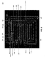
- FIG. 2 illustrates one embodiment of the present invention, where a structure 200 includes a 180° hybrid balun with a built-in rejection filter.
- the balun includes a plurality of folded ⁇ /4 elements, one of which is formed by the traces 201, 202 and 203.
- Each such folded ⁇ /4 element is a quarter wavelength in length, for example, from port P2, to port P3, at the frequency of interest, in this case, 5.3 GHz.
- this embodiment includes four such folded ⁇ /4 elements.
- Ports P2 and P3 are used for differential input.
- Port P4 is connected to ground through a matched (i.e., 50 Ohm) resistance.
- a tap point 209 is a quarter wavelength away from the port P2, and three quarters wavelength away from the port P4, in terms of transmission distance.
- a port P1 is used to connect a single-ended signal. For example, the single-end signal could be connected to an antenna.
- the direction generally from P2 to P1 i.e. left to right in the figure, may be referred to as the horizontal direction, and the perpendicular direction (top to bottom in the figure) may be referred to as the vertical direction, although it will be understood that these designations are nominal.
- the output port P1 is connected to a the tap point 209 through a transmission line (trace) comprised of the traces 204, 205, 206, 207 and 208.
- the transmission distance from the tap point 209 to the output port P1 is a quarter of a wavelength at the frequency f 2 , in this case, 2.4 GHz, i.e., the frequency that needs to be rejected by the filter.
- the transmission line formed by the traces 204-208 represents one pole of the rejection filter. Another pole is represented by the ⁇ /4 transmission line formed by the traces 210, 211, 212, 213, 215 and 216. Note that these traces form a number of folded elements (although in this case not ⁇ /4 elements) such that the total area taken up by the transmission line formed by traces 210-216 is minimized.
- Another pole of the 3-pole rejection filter is formed by the traces 217, 218, 219, 220 and 221, such that the total transmission line length is ⁇ /4 at f 2 , or at 2.4 GHz.
- the distance between the traces needs to be at least twice the thickness of the printed circuit board, to avoid unwanted interference and cross coupling between the traces.
- the folded element formed by the traces 204, 205 and 206 may be thought of as being oriented in the vertical direction.
- the folded element formed by the traces 212, 213 and 214 is oriented in the horizontal direction, as are the folded ⁇ /4 elements of the balun itself.
- FIG. 3 illustrates the S 14 and S 21 transmission parameters of the structure shown in FIG. 2. As illustrated in FIG. 3, there is a minimum at 2.4 GHz, due to the rejection filter "wrapped around" the balun of FIG. 2.
- FIG. 4 illustrates the S 11 transmission parameter of the structure shown in FIG. 2. As shown in FIG. 4, the S 11 parameter at 5.3 GHz is roughly -16 dB, confirming that the structure is matched to the printed circuit board.
- FIG. 5 illustrates the phase response of the device. Of note is the response at 5.3 GHz, which is 180°, as expected of a 180° hybrid balun.
- FIG. 6 shows a photograph of an actual implementation of the device of FIG. 2.
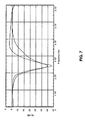
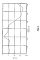
- FIGs. 7-9 illustrate measured responses of the device illustrated in FIG. 6, and confirm that actual performance closely matches the predicted performance of FIGs. 3-5.
- the filter that is wrapped around the balun in FIG. 2 is a 3-pole filter, more or fewer poles may be used (obviously, with a corresponding effect on the filter properties).
- FIG. 2 is believed to provide an optimal design that also minimizes the footprint of the overall device while simultaneously providing for good rejection of unwanted interference from a second frequency of operation.
- the topology may be rearranged to have them on the same side, if needed.
- the balun 200 shown in FIG. 2 may be manufactured on a single layer PCB, where the "bottom" of the PCB is grounded, and the traces shown in FIG. 4 are on the "top.” If additional area reduction is required, the balun 200 of FIG. 2 may be folded further using a third layer of tracing (i.e., using a two-substrate PCB), where the middle tracing layer is ground, and the two halves of the "folded in" balun 200 of FIG. 2 are formed on opposite sides of the PCB.
- a third layer of tracing i.e., using a two-substrate PCB
- the middle tracing layer is ground
- the two halves of the "folded in” balun 200 of FIG. 2 are formed on opposite sides of the PCB.
- Such an arrangement while reducing the area occupied by the balun 200, requires the addition of vias, which tends to increase parasitics, and reduce the bandwidth. Also, to the extent the space on the bottom of the two substrate
Landscapes
- Physics & Mathematics (AREA)
- Electromagnetism (AREA)
- Control Of Motors That Do Not Use Commutators (AREA)
Abstract
Description
| Center frequency of operation | f0 = 5.3 GHz |
| Bandwidth | BW = 0.15 GHz (0.3 dB roll off) |
| Substrate thickness | H = 0.2286mm (top layer) |
| Relative dielectric constant | εr = 3.783 |
| Dielectric loss at 5.3 GHz | tanδ = 0.01 |
| Minimum line width | Δs = 0.127 mm |
| Rejection at 2.4 GHz | R > 20 dB |
Claims (24)
- A balancing/unbalancing (balun) structure for operating at frequency f1 comprising:a microstrip printed circuit board (PCB);a balun on the PCB comprising:two input ports for coupling to a differential signal;an isolated port connected to ground through a matched resistance;an output port for coupling to a single-ended signal corresponding to the differential signal; anda plurality of traces on the PCB connecting the two input ports, the isolated port and a tap point to the output port; andan f2 rejection filter on the PCB wrapped around the balun comprising:a first folded element having a transmission length of λ2/4 and connected to the output port;a second folded element having a transmission length of λ2/4 and connected to the tap point; anda third folded element connecting the tap point to the output port and having a transmission length of λ2/4.
- The balun structure of claim 1, wherein the two input ports and the output port are on opposite sides of the balun structure.
- The balun structure of claim 1, wherein the two input ports and the output port are on the same side of the balun structure.
- The balun structure of claim 1, wherein the balun is a 180° hybrid.
- The balun structure of claim 1, wherein a transmission distance from a first input port of the two ports to a tap point is λ1/4.
- The balun structure of claim 1, wherein the first folded element is oriented in a direction generally corresponding to a direction from the two input ports to the output port.
- The balun structure of claim 1, wherein the third folded element is oriented in a direction generally perpendicular to a direction from the two input ports to the output port.
- The balun structure of claim 1, wherein the second folded element is wrapped around the balun.
- The balun structure of claim 1, wherein distance between adjacent traces is approximately twice PCB thickness.
- The balun structure of claim 1, wherein the PCB includes two substrate layers, two tracing layers and a ground layer, and
wherein the plurality of traces that comprise the balun and the f2 rejection filter are formed on the two tracing layers and are folded over each other. - An f1 balun with an integrated f2 rejection filter comprising:a microstrip line PCB;two input ports for coupling to a differential signal;an isolated port connected to ground through a resistance;an output port for coupling to a single-ended signal corresponding to the differential signal;a plurality of transmission lines on the PCB connecting the two input ports, the isolated port and a tap point forming the balun that is folded in on itself; andthe f2 rejection filter comprising at least one transmission line element wrapped around the plurality of transmission lines.
- The f1 balun of claim 11, wherein the two input ports and the output port are on opposite sides of the balun structure.
- The f1 balun of claim 11, wherein the two input ports and the output port are on the same side of the balun.
- The f1 balun of claim 11, wherein the balun is a 180° hybrid.
- The f1 balun of claim 11, wherein a transmission distance from a first input port of the two ports to a tap point is λ1/4.
- The f1 balun of claim 11, wherein the f2 rejection filter includes a first folded element that is oriented in a direction generally corresponding to a direction from the two input ports to the output port.
- The f1 balun of claim 16, wherein the f2 rejection filter includes a second folded element that is oriented in a direction generally perpendicular to a direction from the two input ports to the output port.
- The f1 balun of claim 11, wherein distance between adjacent transmission lines is approximately twice PCB thickness.
- The f1 balun of claim 11, wherein the plurality of transmission lines includes a plurality of folded λ1/4 elements.
- The f1 balun of claim 11, wherein the at least one transmission line element includes a first folded element having a transmission length of λ2/4 and connected to the output port.
- The f1 balun of claim 20, further including a second folded element having a transmission length of λ2/4 and connected to the tap point.
- The f1 balun of claim 21, wherein the second folded element is wrapped around the plurality of transmission lines.
- The f1 balun of claim 21, wherein the f2 rejection filter further comprises a third folded element connecting the tap point to the output port and having a transmission length of λ2/4.
- A balancing/unbalancing (balun) structure for operating comprising:a balun on a PCB for operating at a first frequency comprising:two input ports for coupling to a differential signal;an isolated port connected to ground through a matched resistance;an output port for coupling to a single-ended signal corresponding to the differential signal; anda plurality of traces on the PCB forming a folded-in on itself balun connecting the two input ports, the isolated port and a tap point to the output port; anda rejection filter for a second frequency wrapped around the balun comprising:a plurality of folded λ2/4 elements connected to the output port; anda folded λ2/4 element connecting the tap point to the output port.
Applications Claiming Priority (2)
| Application Number | Priority Date | Filing Date | Title |
|---|---|---|---|
| US232617 | 2002-09-03 | ||
| US10/232,617 US6791431B2 (en) | 2002-09-03 | 2002-09-03 | Compact balun with rejection filter for 802.11a and 802.11b simultaneous operation |
Publications (2)
| Publication Number | Publication Date |
|---|---|
| EP1396934A1 true EP1396934A1 (en) | 2004-03-10 |
| EP1396934B1 EP1396934B1 (en) | 2010-08-11 |
Family
ID=31715276
Family Applications (1)
| Application Number | Title | Priority Date | Filing Date |
|---|---|---|---|
| EP03019914A Expired - Lifetime EP1396934B1 (en) | 2002-09-03 | 2003-09-02 | Compact balun with rejection filter for 802.11a and 802.11b simultaneous operation |
Country Status (3)
| Country | Link |
|---|---|
| US (1) | US6791431B2 (en) |
| EP (1) | EP1396934B1 (en) |
| DE (1) | DE60333706D1 (en) |
Cited By (1)
| Publication number | Priority date | Publication date | Assignee | Title |
|---|---|---|---|---|
| EP1617560A1 (en) * | 2004-07-15 | 2006-01-18 | Microelectronics Technology | Power amplifier circuit for output terminal of an RFIC |
Families Citing this family (5)
| Publication number | Priority date | Publication date | Assignee | Title |
|---|---|---|---|---|
| US6891448B2 (en) * | 2002-09-03 | 2005-05-10 | Broadcom Corporation | Compact balun for 802.11a applications |
| TWI324852B (en) | 2005-12-08 | 2010-05-11 | Ind Tech Res Inst | A balance to unbalance transformer embedded with a filter |
| CN103904398B (en) * | 2014-03-03 | 2016-06-29 | 华南理工大学 | A kind of miniaturization hybrid ring with filter function |
| CN114814383B (en) * | 2022-03-08 | 2025-08-15 | 浙江大学 | Common-mode absorption type electric field probe and design method thereof |
| CN114725635B (en) * | 2022-05-06 | 2024-01-30 | 华东交通大学 | Dual-frequency balance filter |
Citations (1)
| Publication number | Priority date | Publication date | Assignee | Title |
|---|---|---|---|---|
| US6300919B1 (en) * | 2000-05-23 | 2001-10-09 | Raytheon Company | Highly isolated dual compact stacked spiral antenna |
Family Cites Families (5)
| Publication number | Priority date | Publication date | Assignee | Title |
|---|---|---|---|---|
| DE2144985A1 (en) | 1971-09-08 | 1973-03-15 | Siemens Ag | 3-DB HYBRID CONNECTION IN STRIP LINE TECHNOLOGY |
| US4375699A (en) * | 1981-03-13 | 1983-03-01 | Rockwell International Corporation | Microwave frequency converter with dual balun port |
| US5455545A (en) * | 1993-12-07 | 1995-10-03 | Philips Electronics North America Corporation | Compact low-loss microwave balun |
| FI103614B (en) | 1997-03-20 | 1999-07-30 | Nokia Mobile Phones Ltd | Phasing and balancing means |
| JP3520411B2 (en) | 1999-11-10 | 2004-04-19 | 株式会社村田製作所 | High frequency components using coupled lines |
-
2002
- 2002-09-03 US US10/232,617 patent/US6791431B2/en not_active Expired - Fee Related
-
2003
- 2003-09-02 DE DE60333706T patent/DE60333706D1/en not_active Expired - Lifetime
- 2003-09-02 EP EP03019914A patent/EP1396934B1/en not_active Expired - Lifetime
Patent Citations (1)
| Publication number | Priority date | Publication date | Assignee | Title |
|---|---|---|---|---|
| US6300919B1 (en) * | 2000-05-23 | 2001-10-09 | Raytheon Company | Highly isolated dual compact stacked spiral antenna |
Non-Patent Citations (3)
| Title |
|---|
| JOHNSON, K.M: "X-Band Integrated Circuit Mixer with Reactively Terminated Image", MICROWAVE THEORY AND TECHNIQUES, IEEE TRANSACTIONS ON, vol. 16, no. 7, July 1968 (1968-07-01), pages 388 - 397, XP002265385 * |
| MATSUURA H ET AL: "Monolithic rat-race mixers for millimeter waves", MILLIMETER WAVES, 1997 TOPICAL SYMPOSIUM ON KANAGAWA, JAPAN 7-8 JULY 1997, NEW YORK, NY, USA,IEEE, US, 7 July 1997 (1997-07-07), pages 101 - 104, XP010289059, ISBN: 0-7803-3887-1 * |
| PIERNAS B ET AL: "Improvement of the design of 180 DEG rat-race hybrid", ELECTRONICS LETTERS, IEE STEVENAGE, GB, vol. 36, no. 12, 8 June 2000 (2000-06-08), pages 1035 - 1036, XP006015313, ISSN: 0013-5194 * |
Cited By (1)
| Publication number | Priority date | Publication date | Assignee | Title |
|---|---|---|---|---|
| EP1617560A1 (en) * | 2004-07-15 | 2006-01-18 | Microelectronics Technology | Power amplifier circuit for output terminal of an RFIC |
Also Published As
| Publication number | Publication date |
|---|---|
| US20040041649A1 (en) | 2004-03-04 |
| DE60333706D1 (en) | 2010-09-23 |
| EP1396934B1 (en) | 2010-08-11 |
| US6791431B2 (en) | 2004-09-14 |
Similar Documents
| Publication | Publication Date | Title |
|---|---|---|
| US7420437B2 (en) | Compact balun with rejection filter for 802.11a and 802.11b simultaneous operation | |
| US6133806A (en) | Miniaturized balun transformer | |
| US7528676B2 (en) | Balun circuit suitable for integration with chip antenna | |
| US5697088A (en) | Balun transformer | |
| US6278340B1 (en) | Miniaturized broadband balun transformer having broadside coupled lines | |
| EP1758200B1 (en) | Multilayer planar balun transformer, mixers and amplifiers | |
| US7250828B2 (en) | Compact balun | |
| US6351192B1 (en) | Miniaturized balun transformer with a plurality of interconnecting bondwires | |
| US6636126B1 (en) | Four port hybrid | |
| US6320481B1 (en) | Compact phase shifter circuit using coupled lines | |
| EP0327892B1 (en) | Three-way power splitter using directional couplers | |
| US8248180B2 (en) | Balun with intermediate conductor | |
| US6791431B2 (en) | Compact balun with rejection filter for 802.11a and 802.11b simultaneous operation | |
| US20170026201A1 (en) | Wideband rf device | |
| EP1346432A1 (en) | Four port hybrid microstrip circuit of lange type | |
| US20250112611A1 (en) | Dual-band impedance matching circuit and method of impedance matching | |
| US20240235024A1 (en) | External triple-frequency antenna for unmanned aerial vehicle | |
| CN112886986A (en) | Radio frequency circuit and base station antenna strip line combiner | |
| CN219577026U (en) | Laminated balun suitable for ultrahigh frequency band | |
| US20090051463A1 (en) | Splitter/combiner circuit | |
| EP1845581B1 (en) | Multilayer planar balun transformer, mixers and amplifiers | |
| KR100533907B1 (en) | A Transmission-Line miniaturizing λ/4 Transmission-Line | |
| Roh et al. | Self-Packaged Broadband Rat-Race Coupler With Swapped Ports for Upper Mid-Band Applications | |
| CA2556839C (en) | Multilayer planar balun transformer, mixers and amplifiers | |
| CN115708254A (en) | Filter, duplexer, feed network, and beam forming antenna |
Legal Events
| Date | Code | Title | Description |
|---|---|---|---|
| PUAI | Public reference made under article 153(3) epc to a published international application that has entered the european phase |
Free format text: ORIGINAL CODE: 0009012 |
|
| AK | Designated contracting states |
Kind code of ref document: A1 Designated state(s): AT BE BG CH CY CZ DE DK EE ES FI FR GB GR HU IE IT LI LU MC NL PT RO SE SI SK TR |
|
| AX | Request for extension of the european patent |
Extension state: AL LT LV MK |
|
| 17P | Request for examination filed |
Effective date: 20040910 |
|
| AKX | Designation fees paid |
Designated state(s): DE FR GB |
|
| RAP1 | Party data changed (applicant data changed or rights of an application transferred) |
Owner name: BROADCOM CORPORATION |
|
| 17Q | First examination report despatched |
Effective date: 20090430 |
|
| GRAP | Despatch of communication of intention to grant a patent |
Free format text: ORIGINAL CODE: EPIDOSNIGR1 |
|
| GRAS | Grant fee paid |
Free format text: ORIGINAL CODE: EPIDOSNIGR3 |
|
| GRAA | (expected) grant |
Free format text: ORIGINAL CODE: 0009210 |
|
| AK | Designated contracting states |
Kind code of ref document: B1 Designated state(s): DE FR GB |
|
| REG | Reference to a national code |
Ref country code: GB Ref legal event code: FG4D |
|
| REF | Corresponds to: |
Ref document number: 60333706 Country of ref document: DE Date of ref document: 20100923 Kind code of ref document: P |
|
| PLBE | No opposition filed within time limit |
Free format text: ORIGINAL CODE: 0009261 |
|
| STAA | Information on the status of an ep patent application or granted ep patent |
Free format text: STATUS: NO OPPOSITION FILED WITHIN TIME LIMIT |
|
| REG | Reference to a national code |
Ref country code: FR Ref legal event code: ST Effective date: 20110531 |
|
| 26N | No opposition filed |
Effective date: 20110512 |
|
| PG25 | Lapsed in a contracting state [announced via postgrant information from national office to epo] |
Ref country code: FR Free format text: LAPSE BECAUSE OF NON-PAYMENT OF DUE FEES Effective date: 20101011 |
|
| REG | Reference to a national code |
Ref country code: DE Ref legal event code: R097 Ref document number: 60333706 Country of ref document: DE Effective date: 20110512 |
|
| PGFP | Annual fee paid to national office [announced via postgrant information from national office to epo] |
Ref country code: GB Payment date: 20160927 Year of fee payment: 14 |
|
| REG | Reference to a national code |
Ref country code: DE Ref legal event code: R082 Ref document number: 60333706 Country of ref document: DE Representative=s name: BOSCH JEHLE PATENTANWALTSGESELLSCHAFT MBH, DE Ref country code: DE Ref legal event code: R081 Ref document number: 60333706 Country of ref document: DE Owner name: AVAGO TECHNOLOGIES INTERNATIONAL SALES PTE. LT, SG Free format text: FORMER OWNER: BROADCOM CORP., IRVINE, CALIF., US Ref country code: DE Ref legal event code: R081 Ref document number: 60333706 Country of ref document: DE Owner name: AVAGO TECHNOLOGIES GENERAL IP (SINGAPORE) PTE., SG Free format text: FORMER OWNER: BROADCOM CORP., IRVINE, CALIF., US |
|
| REG | Reference to a national code |
Ref country code: GB Ref legal event code: 732E Free format text: REGISTERED BETWEEN 20171005 AND 20171011 |
|
| GBPC | Gb: european patent ceased through non-payment of renewal fee |
Effective date: 20170902 |
|
| PG25 | Lapsed in a contracting state [announced via postgrant information from national office to epo] |
Ref country code: GB Free format text: LAPSE BECAUSE OF NON-PAYMENT OF DUE FEES Effective date: 20170902 |
|
| REG | Reference to a national code |
Ref country code: DE Ref legal event code: R082 Ref document number: 60333706 Country of ref document: DE Representative=s name: BOSCH JEHLE PATENTANWALTSGESELLSCHAFT MBH, DE Ref country code: DE Ref legal event code: R081 Ref document number: 60333706 Country of ref document: DE Owner name: AVAGO TECHNOLOGIES INTERNATIONAL SALES PTE. LT, SG Free format text: FORMER OWNER: AVAGO TECHNOLOGIES GENERAL IP (SINGAPORE) PTE. LTD., SINGAPORE, SG |
|
| PGFP | Annual fee paid to national office [announced via postgrant information from national office to epo] |
Ref country code: DE Payment date: 20200930 Year of fee payment: 18 |
|
| REG | Reference to a national code |
Ref country code: DE Ref legal event code: R119 Ref document number: 60333706 Country of ref document: DE |
|
| PG25 | Lapsed in a contracting state [announced via postgrant information from national office to epo] |
Ref country code: DE Free format text: LAPSE BECAUSE OF NON-PAYMENT OF DUE FEES Effective date: 20220401 |