EP1396814A1 - Image forming apparatus, optical writing device, and controlling method thereof - Google Patents
Image forming apparatus, optical writing device, and controlling method thereof Download PDFInfo
- Publication number
- EP1396814A1 EP1396814A1 EP03019614A EP03019614A EP1396814A1 EP 1396814 A1 EP1396814 A1 EP 1396814A1 EP 03019614 A EP03019614 A EP 03019614A EP 03019614 A EP03019614 A EP 03019614A EP 1396814 A1 EP1396814 A1 EP 1396814A1
- Authority
- EP
- European Patent Office
- Prior art keywords
- laser
- lasers
- power adjustment
- synchronization signal
- laser beam
- Prior art date
- Legal status (The legal status is an assumption and is not a legal conclusion. Google has not performed a legal analysis and makes no representation as to the accuracy of the status listed.)
- Granted
Links
Images


Classifications
-
- B—PERFORMING OPERATIONS; TRANSPORTING
- B41—PRINTING; LINING MACHINES; TYPEWRITERS; STAMPS
- B41J—TYPEWRITERS; SELECTIVE PRINTING MECHANISMS, i.e. MECHANISMS PRINTING OTHERWISE THAN FROM A FORME; CORRECTION OF TYPOGRAPHICAL ERRORS
- B41J2/00—Typewriters or selective printing mechanisms characterised by the printing or marking process for which they are designed
- B41J2/435—Typewriters or selective printing mechanisms characterised by the printing or marking process for which they are designed characterised by selective application of radiation to a printing material or impression-transfer material
- B41J2/47—Typewriters or selective printing mechanisms characterised by the printing or marking process for which they are designed characterised by selective application of radiation to a printing material or impression-transfer material using the combination of scanning and modulation of light
- B41J2/471—Typewriters or selective printing mechanisms characterised by the printing or marking process for which they are designed characterised by selective application of radiation to a printing material or impression-transfer material using the combination of scanning and modulation of light using dot sequential main scanning by means of a light deflector, e.g. a rotating polygonal mirror
- B41J2/473—Typewriters or selective printing mechanisms characterised by the printing or marking process for which they are designed characterised by selective application of radiation to a printing material or impression-transfer material using the combination of scanning and modulation of light using dot sequential main scanning by means of a light deflector, e.g. a rotating polygonal mirror using multiple light beams, wavelengths or colours
-
- G—PHYSICS
- G06—COMPUTING OR CALCULATING; COUNTING
- G06K—GRAPHICAL DATA READING; PRESENTATION OF DATA; RECORD CARRIERS; HANDLING RECORD CARRIERS
- G06K15/00—Arrangements for producing a permanent visual presentation of the output data, e.g. computer output printers
- G06K15/02—Arrangements for producing a permanent visual presentation of the output data, e.g. computer output printers using printers
- G06K15/12—Arrangements for producing a permanent visual presentation of the output data, e.g. computer output printers using printers by photographic printing, e.g. by laser printers
- G06K15/1204—Arrangements for producing a permanent visual presentation of the output data, e.g. computer output printers using printers by photographic printing, e.g. by laser printers involving the fast moving of an optical beam in the main scanning direction
- G06K15/1209—Intensity control of the optical beam
- G06K15/1214—Intensity control of the optical beam by feedback
-
- H—ELECTRICITY
- H04—ELECTRIC COMMUNICATION TECHNIQUE
- H04N—PICTORIAL COMMUNICATION, e.g. TELEVISION
- H04N1/00—Scanning, transmission or reproduction of documents or the like, e.g. facsimile transmission; Details thereof
- H04N1/04—Scanning arrangements, i.e. arrangements for the displacement of active reading or reproducing elements relative to the original or reproducing medium, or vice versa
- H04N1/047—Detection, control or error compensation of scanning velocity or position
- H04N1/053—Detection, control or error compensation of scanning velocity or position in main scanning direction, e.g. synchronisation of line start or picture elements in a line
-
- H—ELECTRICITY
- H04—ELECTRIC COMMUNICATION TECHNIQUE
- H04N—PICTORIAL COMMUNICATION, e.g. TELEVISION
- H04N1/00—Scanning, transmission or reproduction of documents or the like, e.g. facsimile transmission; Details thereof
- H04N1/04—Scanning arrangements, i.e. arrangements for the displacement of active reading or reproducing elements relative to the original or reproducing medium, or vice versa
- H04N1/113—Scanning arrangements, i.e. arrangements for the displacement of active reading or reproducing elements relative to the original or reproducing medium, or vice versa using oscillating or rotating mirrors
- H04N1/1135—Scanning arrangements, i.e. arrangements for the displacement of active reading or reproducing elements relative to the original or reproducing medium, or vice versa using oscillating or rotating mirrors for the main-scan only
-
- H—ELECTRICITY
- H04—ELECTRIC COMMUNICATION TECHNIQUE
- H04N—PICTORIAL COMMUNICATION, e.g. TELEVISION
- H04N2201/00—Indexing scheme relating to scanning, transmission or reproduction of documents or the like, and to details thereof
- H04N2201/04—Scanning arrangements
- H04N2201/047—Detection, control or error compensation of scanning velocity or position
- H04N2201/04701—Detection of scanning velocity or position
- H04N2201/0471—Detection of scanning velocity or position using dedicated detectors
-
- H—ELECTRICITY
- H04—ELECTRIC COMMUNICATION TECHNIQUE
- H04N—PICTORIAL COMMUNICATION, e.g. TELEVISION
- H04N2201/00—Indexing scheme relating to scanning, transmission or reproduction of documents or the like, and to details thereof
- H04N2201/04—Scanning arrangements
- H04N2201/047—Detection, control or error compensation of scanning velocity or position
- H04N2201/04701—Detection of scanning velocity or position
- H04N2201/04729—Detection of scanning velocity or position in the main-scan direction
-
- H—ELECTRICITY
- H04—ELECTRIC COMMUNICATION TECHNIQUE
- H04N—PICTORIAL COMMUNICATION, e.g. TELEVISION
- H04N2201/00—Indexing scheme relating to scanning, transmission or reproduction of documents or the like, and to details thereof
- H04N2201/04—Scanning arrangements
- H04N2201/047—Detection, control or error compensation of scanning velocity or position
- H04N2201/04701—Detection of scanning velocity or position
- H04N2201/04732—Detecting at infrequent intervals, e.g. once or twice per line for main-scan control
-
- H—ELECTRICITY
- H04—ELECTRIC COMMUNICATION TECHNIQUE
- H04N—PICTORIAL COMMUNICATION, e.g. TELEVISION
- H04N2201/00—Indexing scheme relating to scanning, transmission or reproduction of documents or the like, and to details thereof
- H04N2201/04—Scanning arrangements
- H04N2201/047—Detection, control or error compensation of scanning velocity or position
- H04N2201/04701—Detection of scanning velocity or position
- H04N2201/04744—Detection of scanning velocity or position by detecting the scanned beam or a reference beam
Definitions
- the present invention relates to an optical writing device that includes a plurality of semiconductor lasers and is capable of adjusting amounts of the lasers by using a photo sensing element, a controlling method thereof, and an image forming apparatus including the optical writing device.
- a conventional image forming apparatus equipped with an optical writing device has a laser chip including a light emitting element and a photo sensing element (for example, a photo diode), and a semiconductor laser controller including an optical negative feed back loop for control of the laser chip.
- a number of laser chips and the same number of laser controllers are provided in the image forming apparatus. In the image forming apparatus, control of the different laser chips is performed independently.
- a laser chip which includes a number of light emitting elements arranged in a matrix manner, forming a light emitting element array.
- the pitches in the sub-scan direction between image lines formed on a photo-conducting drum are determined by the characteristics of the lens in the optical system, and, as a result, those devices for making rotations or other complicated adjustments are no longer needed.
- any one of the light emitting elements can be used to detect laser beams that are scanning on the photo-conducting drum and to successively generate synchronization signals.
- the powers (or, the amount of light emitted from a light emitting element) of other light emitting elements are adjusted to a desired value.
- an image forming apparatus comprising: a plurality of lasers, each of the lasers emitting a laser beam including a first part and a second part, the first part of the laser beam from each of the lasers being driven to periodically scan a scanning surface; a first photo detector that detects the second part of the laser beam from each of the lasers and generates a power adjustment signal for determining an output power of the laser; a second photo detector that detects the first part of the laser beam from each of the lasers and generates a scanning synchronization signal corresponding to the laser; and a power adjustment control unit configured to change the output power of each of the lasers to a predetermined value based on the power adjustment signal corresponding to the laser while monitoring the output power of the laser using the corresponding scanning synchronization signal.
- the power adjustment control unit when the power adjustment control unit operates to change (for example, increase) the output power of one of the lasers, the change of the output power of the laser can be monitored by using the scanning synchronization signal. Specifically, the power adjustment control unit determines that the output power of the laser under adjustment reaches the predetermined value when the scanning synchronization signal is detected. This makes it easy to monitor the output power of the laser during adjustment, and ensures reliable power adjustment before the line APC process.
- the power adjustment control unit turns on the lasers one by one and changes the output power of the laser that is on, and in sequence turns off the laser that is on when the scanning synchronization signal corresponding to the laser that is on is detected. More preferably, the power adjustment control unit turns of the laser that is on when the corresponding scanning synchronization signal is detected twice.
- the power adjustment control unit makes the adjustment of changing the output powers of the lasers to the desired value one by one, that is, after completion of adjustment of one laser, start adjustment of the next laser. Further, during the adjustment of one laser, the power adjustment control unit monitors the output power of a laser using the scanning synchronization signal generated by the laser under adjustment itself, but not by any other lasers. Specifically, the power adjustment control unit stops the power adjustment the laser when the scanning synchronization signal is detected twice. Therefore, it makes it simple to initializing the lasers, and makes the time for initializing powers of the lasers short. Further, it is not necessary to stop the power adjustment of any laser in order to generate a common scanning synchronization signal during the adjustment, making the initialization of the image forming apparatus smoothly.
- the number of the lasers adjustable by the power adjustment control unit is changeable.
- the number of the lasers that need to be adjusted can be appropriately changed. As a result, it is possible to make the initialization operation suitable to the system configuration.
- an optical writing device comprising: a plurality of lasers, each of the lasers emitting a laser beam including a first part and a second part, the first part of the laser beam from each of the lasers being driven to periodically scan a scanning surface; a first photo detector that detects the second part of the laser beam from each of the lasers and generates a power adjustment signal for determining an output power of the laser; a second photo detector that detects the first part of the laser beam from each of the lasers and generates a scanning synchronization signal corresponding to the laser; and a power adjustment control unit configured to change the output power of each of the lasers to a predetermined value based on the corresponding power adjustment signal while monitoring the output power of the laser using the corresponding scanning synchronization signal.
- the power adjustment control unit turns on the lasers one by one and changes the output power of the laser that is on, and in sequence turns off the laser that is on when the corresponding scanning synchronisation signal is detected. More, preferably, the power adjustment control unit turns off the laser that is on when the scanning synchronization signal is detected twice.
- a power adjustment method for adjusting output powers of a plurality of lasers in an image forming apparatus wherein each of the lasers emitting a laser beam including a first part and a second part, the first part of the laser beam from each of the lasers being driven to periodically scan a scanning surface
- the power adjustment method comprising the steps of: detecting the first part of the laser beam from each of the lasers and generating a scanning synchronization signal corresponding to the laser; detecting the second part of the laser beam from each of the lasers and generating a power adjustment signal for determining an output powers of the laser; and changing the output power of each of the lasers to a predetermined value based on the power adjustment signal corresponding to the laser while monitoring the output powers of the lasers using the scanning synchronization signal.
- the step of changing the output powers of the lasers to a predetermined value comprises the steps of: turning on the lasers one by one and changing the output power of the laser that is on; and turning off the laser that is on when the scanning synchronization signal is detected. More preferably, the laser that is on is turned of when the scanning synchronization signal is detected twice.
- the image forming apparatus includes a photo sensing element for detecting laser beams emitted from a number of semiconductor lasers, a number of semiconductor laser control circuits each of which has an optical negative feed back loop for controlling a forward current of the corresponding semiconductor laser so as to make an electric signal obtained by converting the laser beam emitted from the corresponding semiconductor laser and detected by the photo sensing element equal to that of a light emitting level designating signal, and an APC (Auto Power Control) timing determination unit for determining the timing of the APC operations of the semiconductor laser control circuits.
- APC Auto Power Control
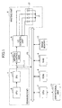
- FIG. 1 is a block diagram showing a schematic configuration of an image forming apparatus according to an embodiment of the present invention.
- the image forming apparatus shown in FIG. 1 includes a scanning unit 1 for reading in data of an original image, and a writing unit 6 for printing the image read by the scanning unit 1 on a medium.
- the scanning unit 1 includes a VPU 2 for converting the input analogue signals corresponding to the original image into digital signals and for performing black offset correction, shading correction, and image position correction, and an IPU 3 performing image processing.
- the writing unit 6 includes a laser diode (LD) array 21 for forming static latent images on a photo-conducting drum, an LD control unit 5 for controlling the LD array 21, and a writing control ASIC (Application Specific Integrated Circuit) 4 for controlling the writing unit 6.
- the image forming apparatus includes a CPU 7 for controlling the image forming apparatus, a ROM 8 in which control programs are stored, a RAM 9 for temporary use of the control programs, an internal system bus 10 for exchanging data between different parts in the image forming apparatus, an interface (I/F) 11 between the system bus 10 and the IPU 3, an image memory 12 for storing the image-read by the scanning unit 1, and an operational unit 13 by which an operator inputs commands.
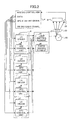
- FIG. 2 shows the writing control ASIC 4 and the LD control unit 5, and a portion of an optical system of the writing unit 6. Shown in FIG. 2 are the writing control ASIC 4, a number of LD control units 5, the LD array 21, a deflector 22 formed by a rotating polygon mirror, an f ⁇ lens 23, a photo-conducting drum 24, and a photo detector 25.
- the LD array 21 includes a photo sensing element 26 and a number of light emitting elements 29.
- Each of the LD control units 5 includes an LD driver 27 and an APC control unit 28.
- the LD array 21 emits multiple laser beams in a forward direction.
- the laser beams are collimated by a not-illustrated collimator lens, deflected by the deflector 22, and are shaped by the f ⁇ lens 23 to form image spots-on the photo-conducting drum 24 which is uniformly charged by a charger. Due to the rotation of the deflector 22, the image spots on the photo-conducting drum 24 scan from side to side repeatedly along the axial direction of the photo-conducting drum 24 (this direction is referred to as the main scan direction). At the same time, the photo-conducting drum 24 is rotating, making the image spots move on the photo-conducting drum 24 along the rotating direction of the photo-conducting drum 24 (this direction is referred to as the sub scan direction).
- the photo detector 25 is arranged out of the laser scanning region to detect the laser beams deflected by the deflector 22 so as to generate a synchronization signal.
- the writing control ASIC 4 applies an image signal to the LD drivers 27 in the semiconductor laser control units 5, and the timing of applying an image signal to the LD drivers 27 is controlled by the synchronization signal generated by the photo detector 25.
- the LD drivers 27 drive the LD array 21 to form a static latent image on the photo-conducting drum 24.
- the static latent image is developed by a developer and is transferred to a paper by a transferring unit.
- Each of the light emitting elements 29 in the LD array 21 also emits a laser beam in the backward direction.
- Each of these laser beams are detected by the photo sensing element 26, and the photo sensing element 26 determines the strength of the incident laser (or power of the corresponding laser).
- the signal generated by the photo sensing element 26 corresponding to the power of the laser is input to APC controller 28 corresponding to the light emitting element 29 that emits the laser beam.
- the APC controller 28 controls the LD drivers 27 according to the output signal from the photo sensing element 26 to make the output power of the light emitting element 29 in the LD array 21 equal to a desired value. Specifically, the power supply of the light emitting element 29 in the LD array 21 is adjusted according to the signal from the photo sensing element 26 so as to the output power of the light emitting element 29 is equal to the desired value. Then the resultant status of the power supply is maintained.
- the output powers of the other light emitting elements 29 are also adjusted in the same way by using the photo sensing element 26 so that the output powers of all the light emitting elements 29 equal to the desired value.
- FIG. 3 is a schematic view showing a configuration of the writing control ASIC 4.
- the writing control ASIC. 4 includes a memory block 31 for converting the speed and the format of the image data from the IPU 3, a unit 32 for processing the image data from the memory block 31, and an output data decoder controller 34 for performing Y transformation on the image data, assignment of P sensor pattern, and so on. Additionally, the output data decoder controller 34 includes an pixel counter 35 for counting the numbers of the light emitting dots of the laser diodes, and a synchronization detection controller 36.
- FIG. 4 is a block diagram showing a configuration of the output data decoder controller 34 of the writing control ASIC 4.
- the output data decoder controller 34 includes a P pattern block 41, a Y transformation block 42, an APC block 43, and an LD ON/OFF block 44.
- the P pattern block 41 extracts data determining process conditions from the data input from the image processing unit 32, and assigns a P sensor pattern for adding toner at a certain density to the photo-conducting drum 24.
- the ⁇ transformation block 42 changes weight factors of data.
- the APC block 43 outputs image data in synchronization with the timing of APC operations for maintaining output powers of the laser diodes to be constant.
- the LD ON/OFF block 44 provides light emitting data for synchronization detection.
- FIGs. 5A through 5M are timing charts showing the operations from the synchronization detection to a line APC operation in the present embodiment, illustrating the initialization operations of the laser diode array 21.
- the laser diode of channel 1 when a synchronization signal is generated twice, the laser diode of channel 1 is turned off, completing the APC operation of channel 1. As shown in FIGS. 5E through 5G, after channel 1 is turned off, channel 2 is turned on, and similarly, when a synchronization signal is generated twice, the laser diode of channel 2 is turned off.
- the laser diodes of four channels are used for writing. Therefore, in the APC operation, first, after the power of the image forming apparatus is turned on, the deflector 22 is rotated, and channel 1 is turned on, and the power of the laser diode of channel 1 is adjusted. When the power of channel 1 is greater than a preset level, the photo detector 25 detects the laser beam and outputs a first synchronization signal. Next, channel 1 is kept to be turned on, and when a second synchronization signal is generated, channel 1 is turned off, and the laser diode in channel 2 is turned on.
- channel 2 when the power of channel 2 is greater than the preset level, the photo detector 25 detects the laser beam and outputs a synchronization signal. Next, channel 2 is kept to be turned on compulsorily, and when the second synchronization signal is generated, channel 2 is turned off, and the laser diode in channel 3 is turned on.
- timing of the line APC operation is determined by using a main scan counter that performs counting using a writing clock signal.
- a value is preset for the main scan counter, and other signals are started or stopped when counts of the main scan counter reach this preset value. By comparing counts of these signals with this preset value, a gate signal is output.
- the preset value may be modified by using, for example, a SP mode, which is capable of modifying various setting data. By using the SP mode, it is also possible to set how many channels of LDs should be adjusted before transferring to the line APC operation, and as a result, it is possible to make the initiation of the LD array suitable to the configuration of the image forming apparatus.
- the output powers of the lasers are monitored using the synchronization signal. This makes it easy to monitor the output powers of the lasers. Further, the adjustments of changing the output powers of lasers to the desired value are made sequentially, and therefore, it is possible to make the time for initializing the laser array short. In addition, the power adjustment is completed when the synchronization signal is detected twice. Therefore, it is not necessary to stop the power adjustment when a synchronization signal is generated, making the initialization of the image forming apparatus smoothly. Further, the number of lasers that need to be adjusted can be appropriately changed. As a result, it is possible to make the initialization operation suitable to a configuration of the image forming apparatus.
Landscapes
- Engineering & Computer Science (AREA)
- Physics & Mathematics (AREA)
- Multimedia (AREA)
- Signal Processing (AREA)
- Optics & Photonics (AREA)
- General Engineering & Computer Science (AREA)
- General Physics & Mathematics (AREA)
- Theoretical Computer Science (AREA)
- Laser Beam Printer (AREA)
- Facsimile Scanning Arrangements (AREA)
- Mechanical Optical Scanning Systems (AREA)
- Fax Reproducing Arrangements (AREA)
Abstract
Description
- The present invention relates to an optical writing device that includes a plurality of semiconductor lasers and is capable of adjusting amounts of the lasers by using a photo sensing element, a controlling method thereof, and an image forming apparatus including the optical writing device.
- In the related art, a conventional image forming apparatus equipped with an optical writing device has a laser chip including a light emitting element and a photo sensing element (for example, a photo diode), and a semiconductor laser controller including an optical negative feed back loop for control of the laser chip. In order to increase printing speed and image quality of the image forming apparatus, a number of laser chips and the same number of laser controllers are provided in the image forming apparatus. In the image forming apparatus, control of the different laser chips is performed independently.
- To increase the printing speed and image quality, a laser chip is proposed which includes a number of light emitting elements arranged in a matrix manner, forming a light emitting element array. In the light emitting element array, because the light emitting elements are arranged at regular intervals, the pitches in the sub-scan direction between image lines formed on a photo-conducting drum are determined by the characteristics of the lens in the optical system, and, as a result, those devices for making rotations or other complicated adjustments are no longer needed.
- In the image forming apparatus of the related art, for example, as disclosed in Japanese Laid Open Patent Application, No. 10-166649, any one of the light emitting elements can be used to detect laser beams that are scanning on the photo-conducting drum and to successively generate synchronization signals. In synchronization with the synchronization signals, the powers (or, the amount of light emitted from a light emitting element) of other light emitting elements are adjusted to a desired value.
- However, with an increasing number of laser chips and in order to further increase the image quality and the printing speed, the machinery for adjusting the pitch between light emitting elements becomes complicated, and a higher speed synchronization detecting device for determining the reference of image starting positions of different channels has to be used.
- When using the light emitting element array including a number of light emitting elements arranged in a matrix manner in a laser chip, because there is only one photo sensing element commonly used by the light emitting elements, it is difficult to perform an APC (Auto Power Control) operation for the light emitting elements at the same time. As a result, it is difficult to employ the APC operation of the related art directly to the light emitting element array configuration used in a multi-beam writing device.
- Further, in the image forming apparatus disclosed in Japanese Laid Open Patent Application, No. 10-166649, when a light emitting element is turned on to generate a synchronization signal, adjustments of other light emitting elements have to be interrupted, and the adjustments have to be monitored constantly.
- It is a general object of the present invention to solve one or more problems of the related art.
- According to a first aspect of the present invention, there is provided an image forming apparatus, comprising: a plurality of lasers, each of the lasers emitting a laser beam including a first part and a second part, the first part of the laser beam from each of the lasers being driven to periodically scan a scanning surface; a first photo detector that detects the second part of the laser beam from each of the lasers and generates a power adjustment signal for determining an output power of the laser; a second photo detector that detects the first part of the laser beam from each of the lasers and generates a scanning synchronization signal corresponding to the laser; and a power adjustment control unit configured to change the output power of each of the lasers to a predetermined value based on the power adjustment signal corresponding to the laser while monitoring the output power of the laser using the corresponding scanning synchronization signal.
- According to the present invention, when the power adjustment control unit operates to change (for example, increase) the output power of one of the lasers, the change of the output power of the laser can be monitored by using the scanning synchronization signal. Specifically, the power adjustment control unit determines that the output power of the laser under adjustment reaches the predetermined value when the scanning synchronization signal is detected. This makes it easy to monitor the output power of the laser during adjustment, and ensures reliable power adjustment before the line APC process.
- Preferably, the power adjustment control unit turns on the lasers one by one and changes the output power of the laser that is on, and in sequence turns off the laser that is on when the scanning synchronization signal corresponding to the laser that is on is detected. More preferably, the power adjustment control unit turns of the laser that is on when the corresponding scanning synchronization signal is detected twice.
- According to the present invention, the power adjustment control unit makes the adjustment of changing the output powers of the lasers to the desired value one by one, that is, after completion of adjustment of one laser, start adjustment of the next laser. Further, during the adjustment of one laser, the power adjustment control unit monitors the output power of a laser using the scanning synchronization signal generated by the laser under adjustment itself, but not by any other lasers. Specifically, the power adjustment control unit stops the power adjustment the laser when the scanning synchronization signal is detected twice. Therefore, it makes it simple to initializing the lasers, and makes the time for initializing powers of the lasers short. Further, it is not necessary to stop the power adjustment of any laser in order to generate a common scanning synchronization signal during the adjustment, making the initialization of the image forming apparatus smoothly.
- Preferably, the number of the lasers adjustable by the power adjustment control unit is changeable.
- According to the present invention, the number of the lasers that need to be adjusted can be appropriately changed. As a result, it is possible to make the initialization operation suitable to the system configuration.
- According to a second aspect of the present invention, there is provided an optical writing device, comprising: a plurality of lasers, each of the lasers emitting a laser beam including a first part and a second part, the first part of the laser beam from each of the lasers being driven to periodically scan a scanning surface; a first photo detector that detects the second part of the laser beam from each of the lasers and generates a power adjustment signal for determining an output power of the laser; a second photo detector that detects the first part of the laser beam from each of the lasers and generates a scanning synchronization signal corresponding to the laser; and a power adjustment control unit configured to change the output power of each of the lasers to a predetermined value based on the corresponding power adjustment signal while monitoring the output power of the laser using the corresponding scanning synchronization signal.
- Preferably, the power adjustment control unit turns on the lasers one by one and changes the output power of the laser that is on, and in sequence turns off the laser that is on when the corresponding scanning synchronisation signal is detected. More, preferably, the power adjustment control unit turns off the laser that is on when the scanning synchronization signal is detected twice.
- According to a third aspect of the present invention, there is provided a power adjustment method for adjusting output powers of a plurality of lasers in an image forming apparatus, wherein each of the lasers emitting a laser beam including a first part and a second part, the first part of the laser beam from each of the lasers being driven to periodically scan a scanning surface, the power adjustment method comprising the steps of: detecting the first part of the laser beam from each of the lasers and generating a scanning synchronization signal corresponding to the laser; detecting the second part of the laser beam from each of the lasers and generating a power adjustment signal for determining an output powers of the laser; and changing the output power of each of the lasers to a predetermined value based on the power adjustment signal corresponding to the laser while monitoring the output powers of the lasers using the scanning synchronization signal.
- Preferably, the step of changing the output powers of the lasers to a predetermined value comprises the steps of: turning on the lasers one by one and changing the output power of the laser that is on; and turning off the laser that is on when the scanning synchronization signal is detected. More preferably, the laser that is on is turned of when the scanning synchronization signal is detected twice.
- These and other objects, features, and advantages of the present invention will become more apparent from the following detailed description of preferred embodiments given with reference to the accompanying drawings.
-
- FIG. 1 is a block diagram showing a schematic configuration of an image forming apparatus according to an embodiment of the present invention;
- FIG. 2 is a block diagram of a controlling
portion of the
writing unit 6, and a schematic view of a portion of the optical system of thewriting unit 6; - FIG. 3 is a schematic view showing a
configuration of the
writing control ASIC 4; - FIG. 4 is a block diagram showing a
configuration of the output
data decoder controller 34 of thewriting control ASIC 4; and - FIGs. 5A through 5M are timing charts showing the operations from the synchronization detection to the line APC operation in the present invention.
-
- Below, preferred embodiments of the present invention are explained with reference to the accompanying drawings.
- In the following descriptions of embodiments of the present invention, the image forming apparatus includes a photo sensing element for detecting laser beams emitted from a number of semiconductor lasers, a number of semiconductor laser control circuits each of which has an optical negative feed back loop for controlling a forward current of the corresponding semiconductor laser so as to make an electric signal obtained by converting the laser beam emitted from the corresponding semiconductor laser and detected by the photo sensing element equal to that of a light emitting level designating signal, and an APC (Auto Power Control) timing determination unit for determining the timing of the APC operations of the semiconductor laser control circuits.
- FIG. 1 is a block diagram showing a schematic configuration of an image forming apparatus according to an embodiment of the present invention.
- The image forming apparatus shown in FIG. 1 includes a
scanning unit 1 for reading in data of an original image, and awriting unit 6 for printing the image read by thescanning unit 1 on a medium. - The
scanning unit 1 includes a VPU 2 for converting the input analogue signals corresponding to the original image into digital signals and for performing black offset correction, shading correction, and image position correction, and anIPU 3 performing image processing. - The
writing unit 6 includes a laser diode (LD)array 21 for forming static latent images on a photo-conducting drum, anLD control unit 5 for controlling theLD array 21, and a writing control ASIC (Application Specific Integrated Circuit) 4 for controlling thewriting unit 6. Additionally, the image forming apparatus includes a CPU 7 for controlling the image forming apparatus, a ROM 8 in which control programs are stored, a RAM 9 for temporary use of the control programs, aninternal system bus 10 for exchanging data between different parts in the image forming apparatus, an interface (I/F) 11 between thesystem bus 10 and theIPU 3, animage memory 12 for storing the image-read by thescanning unit 1, and anoperational unit 13 by which an operator inputs commands. - FIG. 2 shows the
writing control ASIC 4 and theLD control unit 5, and a portion of an optical system of thewriting unit 6. Shown in FIG. 2 are thewriting control ASIC 4, a number ofLD control units 5, theLD array 21, adeflector 22 formed by a rotating polygon mirror, an f lens 23, a photo-conductingdrum 24, and aphoto detector 25. TheLD array 21 includes aphoto sensing element 26 and a number oflight emitting elements 29. Each of theLD control units 5 includes anLD driver 27 and anAPC control unit 28. - The
LD array 21 emits multiple laser beams in a forward direction. The laser beams are collimated by a not-illustrated collimator lens, deflected by thedeflector 22, and are shaped by the f lens 23 to form image spots-on the photo-conductingdrum 24 which is uniformly charged by a charger. Due to the rotation of thedeflector 22, the image spots on the photo-conductingdrum 24 scan from side to side repeatedly along the axial direction of the photo-conducting drum 24 (this direction is referred to as the main scan direction). At the same time, the photo-conductingdrum 24 is rotating, making the image spots move on the photo-conductingdrum 24 along the rotating direction of the photo-conducting drum 24 (this direction is referred to as the sub scan direction). - The
photo detector 25 is arranged out of the laser scanning region to detect the laser beams deflected by thedeflector 22 so as to generate a synchronization signal. Thewriting control ASIC 4 applies an image signal to theLD drivers 27 in the semiconductorlaser control units 5, and the timing of applying an image signal to theLD drivers 27 is controlled by the synchronization signal generated by thephoto detector 25. - The
LD drivers 27 drive theLD array 21 to form a static latent image on the photo-conductingdrum 24. The static latent image is developed by a developer and is transferred to a paper by a transferring unit. - Each of the
light emitting elements 29 in theLD array 21 also emits a laser beam in the backward direction. Each of these laser beams are detected by thephoto sensing element 26, and thephoto sensing element 26 determines the strength of the incident laser (or power of the corresponding laser). The signal generated by thephoto sensing element 26 corresponding to the power of the laser is input toAPC controller 28 corresponding to thelight emitting element 29 that emits the laser beam. - The
APC controller 28 controls theLD drivers 27 according to the output signal from thephoto sensing element 26 to make the output power of thelight emitting element 29 in theLD array 21 equal to a desired value. Specifically, the power supply of thelight emitting element 29 in theLD array 21 is adjusted according to the signal from thephoto sensing element 26 so as to the output power of thelight emitting element 29 is equal to the desired value. Then the resultant status of the power supply is maintained. - The output powers of the other
light emitting elements 29 are also adjusted in the same way by using thephoto sensing element 26 so that the output powers of all thelight emitting elements 29 equal to the desired value. - FIG. 3 is a schematic view showing a configuration of the
writing control ASIC 4. - As shown in FIG. 3, the writing control ASIC. 4 includes a
memory block 31 for converting the speed and the format of the image data from theIPU 3, aunit 32 for processing the image data from thememory block 31, and an outputdata decoder controller 34 for performing Y transformation on the image data, assignment of P sensor pattern, and so on. Additionally, the outputdata decoder controller 34 includes anpixel counter 35 for counting the numbers of the light emitting dots of the laser diodes, and asynchronization detection controller 36. - FIG. 4 is a block diagram showing a configuration of the output
data decoder controller 34 of thewriting control ASIC 4. - The output
data decoder controller 34 includes aP pattern block 41, aY transformation block 42, anAPC block 43, and an LD ON/OFF block 44. - The P pattern block 41 extracts data determining process conditions from the data input from the
image processing unit 32, and assigns a P sensor pattern for adding toner at a certain density to the photo-conductingdrum 24. Theγ transformation block 42 changes weight factors of data. TheAPC block 43 outputs image data in synchronization with the timing of APC operations for maintaining output powers of the laser diodes to be constant. The LD ON/OFF block 44 provides light emitting data for synchronization detection. - FIGs. 5A through 5M are timing charts showing the operations from the synchronization detection to a line APC operation in the present embodiment, illustrating the initialization operations of the
laser diode array 21. - As shown in FIGs. 5A through 5D, the laser diode of
channel 1 is turned on for APC operation, and the laser beam from the laser diode ofchannel 1 is deflected by thedeflector 22 and scans the photo-conductingdrum 24. Each time the laser beam is detected by thephoto detector 25 located in the scanning plane of the laser beam, a synchronization signal is generated. - In the present embodiment, when a synchronization signal is generated twice, the laser diode of
channel 1 is turned off, completing the APC operation ofchannel 1. As shown in FIGS. 5E through 5G, afterchannel 1 is turned off, channel 2 is turned on, and similarly, when a synchronization signal is generated twice, the laser diode of channel 2 is turned off. - This operation is repeated for all channels (FIGS. 5H through 5M show the APC operations for
channel 3 and channel 4), and when a synchronization signal for the laser diode of the last channel is generated twice, the line APC operation for maintaining the output powers of the laser diodes starts in synchronization with the synchronization signal generated bychannel 1. - In the present embodiment, for each main scan operation, the laser diodes of four channels are used for writing. Therefore, in the APC operation, first, after the power of the image forming apparatus is turned on, the
deflector 22 is rotated, andchannel 1 is turned on, and the power of the laser diode ofchannel 1 is adjusted. When the power ofchannel 1 is greater than a preset level, thephoto detector 25 detects the laser beam and outputs a first synchronization signal. Next,channel 1 is kept to be turned on, and when a second synchronization signal is generated,channel 1 is turned off, and the laser diode in channel 2 is turned on. - Similarly, when the power of channel 2 is greater than the preset level, the
photo detector 25 detects the laser beam and outputs a synchronization signal. Next, channel 2 is kept to be turned on compulsorily, and when the second synchronization signal is generated, channel 2 is turned off, and the laser diode inchannel 3 is turned on. - For
channel 3 andchannel 4, the same operations are repeated, and the respective synchronization signals are obtained. When a synchronization signal for the last channel is generated twice, the operation for adjusting the output powers of the laser diodes to the aforementioned desired value is completed. Then the line APC operation for maintaining the output powers of the laser diodes to the desired values starts. Specifically, while the synchronization signal is generated bychannel 1, control transfers to the line APC operation in synchronization with the synchronization signal. - In the present embodiment, timing of the line APC operation is determined by using a main scan counter that performs counting using a writing clock signal. For example, a value is preset for the main scan counter, and other signals are started or stopped when counts of the main scan counter reach this preset value. By comparing counts of these signals with this preset value, a gate signal is output. The preset value may be modified by using, for example, a SP mode, which is capable of modifying various setting data. By using the SP mode, it is also possible to set how many channels of LDs should be adjusted before transferring to the line APC operation, and as a result, it is possible to make the initiation of the LD array suitable to the configuration of the image forming apparatus.
- While the present invention is described with reference to specific embodiments chosen for purpose of illustration, it should be apparent that the invention is not limited to these embodiments, but numerous modifications could be made thereto by those skilled in the art without departing from the basic concept and scope of the invention.
- Summarizing the effects of the present invention, during APC operation for adjusting output powers of lasers in a laser array, the output powers of the lasers are monitored using the synchronization signal. This makes it easy to monitor the output powers of the lasers. Further, the adjustments of changing the output powers of lasers to the desired value are made sequentially, and therefore, it is possible to make the time for initializing the laser array short. In addition, the power adjustment is completed when the synchronization signal is detected twice. Therefore, it is not necessary to stop the power adjustment when a synchronization signal is generated, making the initialization of the image forming apparatus smoothly. Further, the number of lasers that need to be adjusted can be appropriately changed. As a result, it is possible to make the initialization operation suitable to a configuration of the image forming apparatus.
- This patent application is based on Japanese Priority Patent Application No. 2002-260518 filed on September 5, 2002, the entire contents of which are hereby incorporated by reference.
Claims (25)
- An image forming apparatus, comprising:a plurality of lasers, each of the lasers emitting a laser beam including a first part and a second part, the first part of the laser beam from each of the lasers being driven to periodically scan a scanning surface;a first photo detector that detects the second part of the laser beam from each of the lasers and generates a power adjustment signal for determining an output power of the laser;a second photo detector that detects the first part of the laser beam from each of the lasers and generates a scanning synchronization signal corresponding to the laser; anda power adjustment control unit configured to change the output power of each of the lasers to a predetermined value based on the power adjustment signal corresponding to the laser while monitoring the output power of the laser using the corresponding scanning synchronization signal.
- The image forming apparatus as claimed in claim 1, wherein the power adjustment control unit turns on the lasers one by one and changes the output power of the laser that is on, and in sequence turns off the laser that is on when the scanning synchronization signal corresponding to the laser that is on is detected.
- The image forming apparatus as claimed in claim 2, wherein the power adjustment control unit turns off the laser that is on when the scanning synchronization signal corresponding to the laser that is on is detected twice.
- The image forming apparatus as claimed in claim 1, wherein the second photo detector generates one scanning synchronization signal in one scanning period.
- The image forming apparatus as claimed in claim 1, wherein a number of the lasers adjustable by the power adjustment control unit is changeable.
- An optical writing device, comprising:a plurality of lasers, each of the lasers emitting a laser beam including a first part and a second part, the first part of the laser beam from each of the lasers being driven to periodically scan a scanning surface;a first photo detector that detects the second part of the laser beam from each of the lasers and generates a power adjustment signal for determining an output power of the laser;a second photo detector that detects the first part of the laser beam from each of the lasers and generates a scanning synchronization signal corresponding to the laser; anda power adjustment control unit configured to change the output power of each of the lasers to a predetermined value based on the corresponding power adjustment signal while monitoring the output power of the laser using the corresponding scanning synchronization signal.
- The optical writing device as claimed in claim 6, wherein the power adjustment control unit turns on the lasers one by one and changes the output power of the laser that is on, and in sequence turns off the laser that is on when the scanning synchronization signal corresponding to the laser that is on is detected.
- The optical writing device as claimed in claim 7, wherein the power adjustment control unit turns off the laser that is on when the scanning synchronization signal corresponding to the laser that is on is detected twice.
- The image forming apparatus as claimed in claim 6, wherein the second photo detector generates one scanning synchronization signal in one scanning period.
- The optical writing device as claimed in claim 6, wherein a number of the lasers adjustable by the power adjustment control unit is changeable.
- A power adjustment method for adjusting output powers of a plurality of lasers in an image forming apparatus, wherein each of the lasers emitting a laser beam including a first part and a second part, the first part of the laser beam from each of the lasers being driven to periodically scan a scanning surface, the power adjustment method comprising the steps of:detecting the first part of the laser beam from each of the lasers and generating a scanning synchronization signal corresponding to the laser;detecting the second part of the laser beam from each of the lasers and generating a power adjustment signal for determining an output powers of the laser; andchanging the output power of each of the lasers to a predetermined value based on the power adjustment signal corresponding to the laser while monitoring the output powers of the lasers using the scanning synchronization signal.
- The power adjustment method as claimed in claim 11, wherein the step of changing the output powers of the lasers to a predetermined value comprises the steps of:turning on the lasers one by one and changing the output power of the laser that is on; andturning off, in sequence, the laser that is on when the scanning synchronization signal is detected.
- The power adjustment method as claimed in claim 12, wherein in the step of turning off the laser that is on, the laser that is on is turned of when the scanning synchronization signal is detected twice.
- The power adjustment method as claimed in claim 11, wherein one scanning synchronization signal is generated in one scanning period.
- The power adjustment method as claimed in claim 11, wherein a number of the lasers whose output powers are adjustable is changeable.
- An image forming apparatus, comprising:a plurality of lasers, each of the lasers emitting a laser beam including a first part and a second part, the first part of the laser beam from each of the lasers being driven to periodically scan a scanning surface;a first photo detection means for detecting the second part of the laser beam from each of the lasers and generating a power adjustment signal used for determining an output power of the laser;a second photo detection means for detecting the first part of the laser beam from each of the lasers and generating a scanning synchronization signal corresponding to the laser; anda power adjustment control means for changing the output power of each of the lasers to a predetermined value based on the power adjustment signals corresponding to the laser while monitoring the output power of the lasers using the corresponding scanning synchronization signal.
- The image forming apparatus as claimed in claim 16, wherein the power adjustment control means turns on the lasers one by one and changes the output power of the laser that is on, and in sequence turns off the laser that is on when the corresponding scanning synchronization signal is detected.
- The image forming apparatus as claimed in claim 17, wherein the power adjustment control means turns off the laser that is on when the corresponding scanning synchronization signal is detected twice.
- The image forming apparatus as claimed in claim 16, wherein the second photo detection means generates one scanning synchronization signal in one scanning period.
- The image forming apparatus as claimed in claim 16, wherein a number of the lasers adjustable by the power adjustment control means is changeable.
- An optical writing device, comprising:a plurality of lasers, each of the lasers emitting a laser beam including a first part and a second part, the first part of the laser beam from each of the lasers being driven to periodically scan a scanning surface;a first photo detection means for detecting the second part of the laser beam from each of the lasers and generating a power adjustment signal used for determining an output power of the laser;a second photo detection means for detecting the first part of the laser beam from each of the lasers and generating a scanning synchronization signal corresponding to the laser; anda power adjustment control means for changing the output power of each of the lasers to a predetermined value based on the power adjustment signals corresponding to the laser while monitoring the output power of the lasers using the corresponding scanning synchronization signal.
- The optical writing device as claimed in claim 21, wherein the power adjustment control means turns on the lasers one by one and changes the output power of the laser that is on, and in sequence turns off the laser that is on when the scanning synchronization signal is detected.
- The optical writing device as claimed in claim 22, wherein the power adjustment control means turns of laser that is on when the scanning synchronization signal is detected twice.
- The optical writing device as claimed in claim 21, wherein the second photo detection means generates one scanning synchronization signal in one scanning period.
- The optical writing device as claimed in claim 21, wherein a number of the lasers adjustable by the power adjustment control means is changeable.
Applications Claiming Priority (2)
| Application Number | Priority Date | Filing Date | Title |
|---|---|---|---|
| JP2002260518A JP2004101656A (en) | 2002-09-05 | 2002-09-05 | Image forming apparatus, optical writing apparatus, and APC control method for optical writing apparatus |
| JP2002260518 | 2002-09-05 |
Publications (2)
| Publication Number | Publication Date |
|---|---|
| EP1396814A1 true EP1396814A1 (en) | 2004-03-10 |
| EP1396814B1 EP1396814B1 (en) | 2005-08-24 |
Family
ID=31712330
Family Applications (1)
| Application Number | Title | Priority Date | Filing Date |
|---|---|---|---|
| EP03019614A Expired - Lifetime EP1396814B1 (en) | 2002-09-05 | 2003-09-04 | Image forming apparatus, optical writing device, and controlling method thereof |
Country Status (5)
| Country | Link |
|---|---|
| US (1) | US6998603B2 (en) |
| EP (1) | EP1396814B1 (en) |
| JP (1) | JP2004101656A (en) |
| DE (1) | DE60301376T2 (en) |
| ES (1) | ES2246032T3 (en) |
Cited By (3)
| Publication number | Priority date | Publication date | Assignee | Title |
|---|---|---|---|---|
| CN102394469A (en) * | 2010-07-15 | 2012-03-28 | 株式会社理光 | Semiconductor laser driver and image forming apparatus incorporating same |
| WO2018009069A1 (en) | 2016-07-08 | 2018-01-11 | Tocano Holding B.V. | Printing apparatus with improved print quality control |
| NL2017142B1 (en) * | 2016-07-08 | 2018-01-15 | Tocano Holding B V | Printing apparatus with improved print quality control |
Families Citing this family (8)
| Publication number | Priority date | Publication date | Assignee | Title |
|---|---|---|---|---|
| US20050134679A1 (en) * | 2003-12-04 | 2005-06-23 | Paterson Robert L. | Margin registration of a scan line in an electrophotographic printer |
| US6861721B1 (en) * | 2003-12-08 | 2005-03-01 | Texas Instruments Incorporated | Barrier region and method for wafer scale package (WCSP) devices |
| JP4487752B2 (en) * | 2004-12-07 | 2010-06-23 | リコープリンティングシステムズ株式会社 | Multi-beam image forming apparatus |
| JP2006315278A (en) * | 2005-05-12 | 2006-11-24 | Canon Inc | Image forming apparatus |
| KR100694139B1 (en) | 2005-07-13 | 2007-03-12 | 삼성전자주식회사 | Optical fiber device and method |
| JP4570156B2 (en) * | 2005-08-24 | 2010-10-27 | 株式会社リコー | Image forming apparatus |
| US8217975B2 (en) * | 2008-04-01 | 2012-07-10 | Xerox Corporation | Apparatus for forming an image and corresponding methods |
| US9667022B1 (en) | 2014-08-01 | 2017-05-30 | Nlight, Inc. | Distributed laser power architecture for laser diode arrays |
Citations (3)
| Publication number | Priority date | Publication date | Assignee | Title |
|---|---|---|---|---|
| US4933549A (en) * | 1987-12-11 | 1990-06-12 | Ricoh Company, Ltd. | Light beam scanning apparatus |
| JPH10166649A (en) | 1996-12-13 | 1998-06-23 | Canon Inc | APC control pull-in method and image forming apparatus |
| US6246463B1 (en) * | 1998-05-08 | 2001-06-12 | Minolta Co., Ltd. | Optical laser scanning device and image forming apparatus having the optical laser scanning device |
Family Cites Families (5)
| Publication number | Priority date | Publication date | Assignee | Title |
|---|---|---|---|---|
| US5726437A (en) * | 1994-10-27 | 1998-03-10 | Fuji Xerox Co., Ltd. | Light intensity control device |
| JP3276284B2 (en) * | 1996-01-12 | 2002-04-22 | 旭光学工業株式会社 | Multi-beam optical scanning device |
| US6114682A (en) * | 1997-08-27 | 2000-09-05 | Asahi Kogaku Kogyo Kabushiki Kaisha | Apparatus and method for controlling light intensity |
| JP2001147387A (en) * | 1999-11-22 | 2001-05-29 | Asahi Optical Co Ltd | Scanning optical device |
| JP2001150726A (en) | 1999-11-30 | 2001-06-05 | Ricoh Co Ltd | Optical writing device |
-
2002
- 2002-09-05 JP JP2002260518A patent/JP2004101656A/en active Pending
-
2003
- 2003-09-04 US US10/653,893 patent/US6998603B2/en not_active Expired - Fee Related
- 2003-09-04 EP EP03019614A patent/EP1396814B1/en not_active Expired - Lifetime
- 2003-09-04 DE DE60301376T patent/DE60301376T2/en not_active Expired - Lifetime
- 2003-09-04 ES ES03019614T patent/ES2246032T3/en not_active Expired - Lifetime
Patent Citations (3)
| Publication number | Priority date | Publication date | Assignee | Title |
|---|---|---|---|---|
| US4933549A (en) * | 1987-12-11 | 1990-06-12 | Ricoh Company, Ltd. | Light beam scanning apparatus |
| JPH10166649A (en) | 1996-12-13 | 1998-06-23 | Canon Inc | APC control pull-in method and image forming apparatus |
| US6246463B1 (en) * | 1998-05-08 | 2001-06-12 | Minolta Co., Ltd. | Optical laser scanning device and image forming apparatus having the optical laser scanning device |
Cited By (4)
| Publication number | Priority date | Publication date | Assignee | Title |
|---|---|---|---|---|
| CN102394469A (en) * | 2010-07-15 | 2012-03-28 | 株式会社理光 | Semiconductor laser driver and image forming apparatus incorporating same |
| WO2018009069A1 (en) | 2016-07-08 | 2018-01-11 | Tocano Holding B.V. | Printing apparatus with improved print quality control |
| NL2017142B1 (en) * | 2016-07-08 | 2018-01-15 | Tocano Holding B V | Printing apparatus with improved print quality control |
| CN109689376A (en) * | 2016-07-08 | 2019-04-26 | 托卡诺控股有限公司 | Printing equipment with the control of improved print quality |
Also Published As
| Publication number | Publication date |
|---|---|
| ES2246032T3 (en) | 2006-02-01 |
| US6998603B2 (en) | 2006-02-14 |
| DE60301376T2 (en) | 2006-06-08 |
| EP1396814B1 (en) | 2005-08-24 |
| US20040119003A1 (en) | 2004-06-24 |
| JP2004101656A (en) | 2004-04-02 |
| DE60301376D1 (en) | 2005-09-29 |
Similar Documents
| Publication | Publication Date | Title |
|---|---|---|
| EP1396814A1 (en) | Image forming apparatus, optical writing device, and controlling method thereof | |
| US20160246208A1 (en) | Image forming apparatus that forms latent image by irradiating photosensitive member with light | |
| US20090190944A1 (en) | Optical scanner, image forming apparatus, and image forming method | |
| US20130127975A1 (en) | Image forming apparatus and image forming method | |
| US6496213B1 (en) | Multi-beam control method | |
| EP1111903B1 (en) | An optical writing apparatus and method | |
| CN1068447C (en) | Exposing device | |
| JPH0969662A (en) | Light intensity modulation circuit for optical scanning device | |
| EP0581259A2 (en) | Image forming apparatus and light quantity control device for use in the image forming apparatus | |
| JP4265186B2 (en) | Light source control device | |
| US8125504B2 (en) | Image forming apparatus and control program of image forming apparatus | |
| US6879334B2 (en) | Image forming apparatus capable of controlling write start position of each beam | |
| JPH10108019A (en) | Image processing method, apparatus and medium | |
| US7804514B2 (en) | Light beam scanning apparatus and image forming apparatus | |
| JP2005010580A (en) | Light source controller | |
| JP2001293903A (en) | Image forming device | |
| JP2004345113A (en) | Optical writing device | |
| JP2000118040A (en) | Image forming device | |
| JP2002149034A (en) | Image forming device | |
| JP2002067377A (en) | Image forming apparatus and control method thereof | |
| JP2005193452A (en) | Optical writing apparatus and digital copying machine | |
| JP2005238660A (en) | Optical writing apparatus and image forming apparatus | |
| JPS63172287A (en) | Method for correcting light quantity of light emitting diode array | |
| JPH10166644A (en) | Image forming device | |
| JP2006058631A (en) | Optical writing apparatus and digital copying machine |
Legal Events
| Date | Code | Title | Description |
|---|---|---|---|
| PUAI | Public reference made under article 153(3) epc to a published international application that has entered the european phase |
Free format text: ORIGINAL CODE: 0009012 |
|
| 17P | Request for examination filed |
Effective date: 20030904 |
|
| AK | Designated contracting states |
Kind code of ref document: A1 Designated state(s): AT BE BG CH CY CZ DE DK EE ES FI FR GB GR HU IE IT LI LU MC NL PT RO SE SI SK TR |
|
| AX | Request for extension of the european patent |
Extension state: AL LT LV MK |
|
| 17Q | First examination report despatched |
Effective date: 20040621 |
|
| AKX | Designation fees paid |
Designated state(s): DE ES FR GB IT NL |
|
| GRAP | Despatch of communication of intention to grant a patent |
Free format text: ORIGINAL CODE: EPIDOSNIGR1 |
|
| GRAS | Grant fee paid |
Free format text: ORIGINAL CODE: EPIDOSNIGR3 |
|
| GRAA | (expected) grant |
Free format text: ORIGINAL CODE: 0009210 |
|
| AK | Designated contracting states |
Kind code of ref document: B1 Designated state(s): DE ES FR GB IT NL |
|
| REG | Reference to a national code |
Ref country code: GB Ref legal event code: FG4D |
|
| REF | Corresponds to: |
Ref document number: 60301376 Country of ref document: DE Date of ref document: 20050929 Kind code of ref document: P |
|
| REG | Reference to a national code |
Ref country code: ES Ref legal event code: FG2A Ref document number: 2246032 Country of ref document: ES Kind code of ref document: T3 |
|
| ET | Fr: translation filed | ||
| PLBE | No opposition filed within time limit |
Free format text: ORIGINAL CODE: 0009261 |
|
| STAA | Information on the status of an ep patent application or granted ep patent |
Free format text: STATUS: NO OPPOSITION FILED WITHIN TIME LIMIT |
|
| 26N | No opposition filed |
Effective date: 20060526 |
|
| REG | Reference to a national code |
Ref country code: FR Ref legal event code: PLFP Year of fee payment: 14 |
|
| PGFP | Annual fee paid to national office [announced via postgrant information from national office to epo] |
Ref country code: GB Payment date: 20160920 Year of fee payment: 14 Ref country code: NL Payment date: 20160920 Year of fee payment: 14 Ref country code: DE Payment date: 20160921 Year of fee payment: 14 |
|
| PGFP | Annual fee paid to national office [announced via postgrant information from national office to epo] |
Ref country code: FR Payment date: 20160921 Year of fee payment: 14 |
|
| PGFP | Annual fee paid to national office [announced via postgrant information from national office to epo] |
Ref country code: ES Payment date: 20160916 Year of fee payment: 14 |
|
| PGFP | Annual fee paid to national office [announced via postgrant information from national office to epo] |
Ref country code: IT Payment date: 20160922 Year of fee payment: 14 |
|
| REG | Reference to a national code |
Ref country code: DE Ref legal event code: R119 Ref document number: 60301376 Country of ref document: DE |
|
| REG | Reference to a national code |
Ref country code: NL Ref legal event code: MM Effective date: 20171001 |
|
| GBPC | Gb: european patent ceased through non-payment of renewal fee |
Effective date: 20170904 |
|
| PG25 | Lapsed in a contracting state [announced via postgrant information from national office to epo] |
Ref country code: NL Free format text: LAPSE BECAUSE OF NON-PAYMENT OF DUE FEES Effective date: 20171001 |
|
| REG | Reference to a national code |
Ref country code: FR Ref legal event code: ST Effective date: 20180531 |
|
| PG25 | Lapsed in a contracting state [announced via postgrant information from national office to epo] |
Ref country code: DE Free format text: LAPSE BECAUSE OF NON-PAYMENT OF DUE FEES Effective date: 20180404 Ref country code: GB Free format text: LAPSE BECAUSE OF NON-PAYMENT OF DUE FEES Effective date: 20170904 |
|
| PG25 | Lapsed in a contracting state [announced via postgrant information from national office to epo] |
Ref country code: FR Free format text: LAPSE BECAUSE OF NON-PAYMENT OF DUE FEES Effective date: 20171002 Ref country code: IT Free format text: LAPSE BECAUSE OF NON-PAYMENT OF DUE FEES Effective date: 20170904 |
|
| REG | Reference to a national code |
Ref country code: ES Ref legal event code: FD2A Effective date: 20181024 |
|
| PG25 | Lapsed in a contracting state [announced via postgrant information from national office to epo] |
Ref country code: ES Free format text: LAPSE BECAUSE OF NON-PAYMENT OF DUE FEES Effective date: 20170905 |