EP1394937A2 - Switching circuit - Google Patents
Switching circuit Download PDFInfo
- Publication number
- EP1394937A2 EP1394937A2 EP03255291A EP03255291A EP1394937A2 EP 1394937 A2 EP1394937 A2 EP 1394937A2 EP 03255291 A EP03255291 A EP 03255291A EP 03255291 A EP03255291 A EP 03255291A EP 1394937 A2 EP1394937 A2 EP 1394937A2
- Authority
- EP
- European Patent Office
- Prior art keywords
- signal source
- load circuit
- switching
- signal
- circuit
- Prior art date
- Legal status (The legal status is an assumption and is not a legal conclusion. Google has not performed a legal analysis and makes no representation as to the accuracy of the status listed.)
- Withdrawn
Links
Images


Classifications
-
- H—ELECTRICITY
- H03—ELECTRONIC CIRCUITRY
- H03G—CONTROL OF AMPLIFICATION
- H03G3/00—Gain control in amplifiers or frequency changers
- H03G3/20—Automatic control
- H03G3/30—Automatic control in amplifiers having semiconductor devices
- H03G3/34—Muting amplifier when no signal is present
- H03G3/348—Muting in response to a mechanical action or to power supply variations, e.g. during tuning; Click removal circuits
Definitions
- the present invention relates to a switching circuit for switching a load circuit connected to a signal source.
- FIG. 5 shows a conventional switching cir cuit.
- a signal output from a signal source 11 is provided to a load circuit 13 or 14 via switching means 12.
- the switching means 12 is the one structured by a switch circuit of a single-pole double-throw type, for example.
- the input terminal 12a is connected to either the output terminal 12b or 12c.
- the input terminal 12a is currently connected to the output terminal 12b but is to be connected to the output terminal 12c, it takes about 1 ⁇ S (micro second) for the input terminal 12a to be cut off from the output terminal 12b and connected to the output terminal 12c.
- the input terminal 12a is connected neither the output terminal 12b nor 12c.
- An object of the present invention is to reduce signal emission in a switching period, successfully causing less impact on other circuits, and stabilizing a signal source.
- a switching circuit comprising a signal source, and switching means for connecting the signal source to a first load circuit or a second load circuit.
- Emission attenuation means is also provided for attenuating a signal to be emitted from the switching means between the signal source and the switching means in a time period at least between the signal source being cut off from either the first or second load circuit and being connected to the other.
- the emission attenuation means includes a third load circuit, and the third load circuit is connected to the signal source in a time period at least before the signal source being cut off from either the first or second load circuit to after being connected to the other.
- an impedance of the third load circuit is so set as to be almost an average value between an impedance of the first load circuit and an impedance of the second load circuit.
- the emission attenuation means includes an amplifier, and a gain of the amplifier is attenuated in the time period at least before the signal source being cut off from either the first or second load circuit to after being connected to the other.
- the gain of the amplifier is attenuated by changing a bias voltage of an amplification element in the amplifier.
- the signal source is structured by a voltage control oscillator.
- FIG. 1 shows a switching circuit in a first embodiment of the present invention.
- a signal output from a signal source 1 is provided to a first load circuit 3 or a second load circuit 4 via switching means 2.
- the signal source 1 is structured by a voltage control oscillator, for example.
- the switching means 2 is the one structured by a switch circuit of a single-pole double-throw type, for example.
- the input terminal 2a is connected to either the output terminal 2b or 2c.
- the input terminal 2a In a case where the input terminal 2a is connected to the output terminal 2b but is to be connected to the output terminal 2c, it takes about 1 ⁇ S (micro second) for the input terminal 2a to be cut off from the output terminal 2b and connected to the output terminal 2c. During this switching period, the input terminal 2a is connected neither the output terminal 2b nor 2c.
- the emission attenuation means 5 includes open/close means 5a and a third load circuit 5b, those of which are connected serially.
- the third load circuit 5b is preferably about the same in impedance with the first and second load circuits 3 and 4. Although the first and second load circuits 3 and 4 are generally equal in impedance, if different, the values are averaged for use therefor .
- the open/close means 5a is generally open, and responding to a switching signal coming from a switching control circuit 6, temporarily closes in synchronization with the switching operation of the switching means 2.
- the switching means 2 will be closed in a time period from immediately before the cut-off, e.g., time to 0.2 ⁇ S before, to immediately after time t2, e.g., time t3 0.2 ⁇ S after, at which the connection is established with the output terminal 2c. Therefore, the temporal change of the load circuit connected to the signal source 1 looks as shown in FIG. 2.
- the first and third load circuits 3 and 5b are both connected to the signal source 1 in a time period from time to to time t1, and in a time period from times t2 to t3, connected are the second and third load circuits 4 and 5b.
- the input terminal 2a of the switching means 2 never opens, and thus a half the impedance of the connected two load circuits will do to terminate. This reduces the load fluctuation of the signal source, and as a result, the signal emission from the input terminal 2a is decreased. Further, using a voltage control oscillator as the signal source 1 will also reduce the load fluctuation, leading to less fluctuation of the oscillation frequency. What is better, the input terminal 2a does not open so that the reflection amount toward the signal source 1 is reduced. Thus, the signal source 1 operates stably.
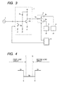
- FIG. 3 shows a second embodiment.
- emission attenuation means 7 which includes an amplifier 7a and open/close means 7b for switching base bias voltage of an amplification element TR in the amplifier 7a.
- an output terminal is connected to the input terminal 2a of the switching means 2.
- the open/close means 7b is generally open, but temporarily closed in synchronization with the switching operation of the switching means 2 in response to a switching signal coming from the switching control circuit 6.
- the switching means 2 will be closed in a time period from immediately before the cut-off, e.g., time to 0.2 ⁇ S before, to immediately after time t2, e.g., time t3 0.2 ⁇ S after, at which the connection is established with the output terminal 2c. Therefore, in the time period, the base bias voltage of the amplification element TR is reduced, leading gain attenuation.
- the temporal change of the gain looks as shown in FIG. 4. As is known therefrom, the gain remains G1 to time t0, is reduced to G2 from time t0 to t3, and is increased to G1 after time t3.
- the signal emission from the input terminal 2a is reduced in level.
- the signal source 1 does not suffer large load fluctuation, and the reflection toward the signal source 1 is small in amount.
- the signal source 1 operates stably.
- the switching circuit of the present invention is provided with switching means for connecting a signal source to a first load circuit or a second load circuit.
- Emission attenuation means is provided for attenuating a signal to be emitted from the switching means is provided between the signal source and the switching means in a time period between the signal source being cut off from either the first or second load circuit and being connected to the other. Accordingly, this stops signal jumping to other circuits, successfully reducing the signal level, and preventing other circuits from being blocked.
- the emission attenuation means includes a third load circuit, and the third load circuit is connected to the signal source in a time period at least before the signal source being cut off from either the first or second load circuit to after being connected to the other. Therefore, the signal source never opens, successfully not receiving large load fluctuation, and operating stably.
- an impedance of the third load circuit is so set as to be almost an average value between an impedance of the first load circuit and an impedance of the second load circuit.
- the emission attenuation means includes an amplifier, and a gain of the amplifier is attenuated in the time period at least before the signal source being cut off from either the first or second load circuit to after being connected to the other. This reduces signal emission in the switching period, successfully reducing the load fluctuation to the signal source side.
- the gain of the amplifier is attenuated by changing a bias voltage of an amplification element in the amplifier. This makes the gain change easier.
- the signal source is structured by a voltage control oscillator. Accordingly, no fluctuation occurs to the oscillation frequency in a time period for load circuit change.
Landscapes
- Electronic Switches (AREA)
- Oscillators With Electromechanical Resonators (AREA)
Abstract
Description
Claims (6)
- A switching circuit, comprising
a signal source; and
switching means for connecting the signal source to a first load circuit or a second load circuit, wherein
between the signal source and the switching means, emission attenuation means is provided for attenuating a signal to be emitted from the switching means in a time period at least between the signal source being cut off from either the first or second load circuit and being connected to the other. - The switching circuit according to claim 1, wherein the emission attenuation means includes a third load circuit, and the third load circuit is connected to the signal source in a time period at least before the signal source being cut off from either the first or second load circuit to after being connected to the other.
- The switching circuit according to claim 2, wherein an impedance of the third load circuit is so set as to be almost an average value between an impedance of the first load circuit and an impedance of the second load circuit.
- The switching circuit according to claim 1, wherein the emission attenuation means includes an amplifier, and a gain of the amplifier is attenuated in a time period at least before the signal source being cut off from either the first or second load circuit to after being connected to the other.
- The switching circuit according to claim 4, wherein the gain of the amplifier is attenuated by changing a bias voltage of an amplification element in the amplifier.
- The switching circuit according to any one of claims 1 to 5, wherein the signal source is structured by a voltage control oscillator.
Applications Claiming Priority (2)
| Application Number | Priority Date | Filing Date | Title |
|---|---|---|---|
| JP2002246511A JP2004088400A (en) | 2002-08-27 | 2002-08-27 | Switching circuit |
| JP2002246511 | 2002-08-27 |
Publications (2)
| Publication Number | Publication Date |
|---|---|
| EP1394937A2 true EP1394937A2 (en) | 2004-03-03 |
| EP1394937A3 EP1394937A3 (en) | 2006-12-27 |
Family
ID=31492533
Family Applications (1)
| Application Number | Title | Priority Date | Filing Date |
|---|---|---|---|
| EP03255291A Withdrawn EP1394937A3 (en) | 2002-08-27 | 2003-08-26 | Switching circuit |
Country Status (2)
| Country | Link |
|---|---|
| EP (1) | EP1394937A3 (en) |
| JP (1) | JP2004088400A (en) |
Family Cites Families (4)
| Publication number | Priority date | Publication date | Assignee | Title |
|---|---|---|---|---|
| US4808859A (en) * | 1987-01-09 | 1989-02-28 | American Electronic Laboratories, Inc. | Broadband electronic switch |
| US5075569A (en) * | 1989-03-17 | 1991-12-24 | Tektronix, Inc. | Output device circuit and method to minimize impedance fluctuations during crossover |
| JP2801563B2 (en) * | 1994-08-30 | 1998-09-21 | 松下電器産業株式会社 | Transmission / reception circuit of communication radio, semiconductor integrated circuit device, and communication radio |
| JP4119038B2 (en) * | 1999-05-27 | 2008-07-16 | Necエレクトロニクス株式会社 | High frequency switching circuit IC |
-
2002
- 2002-08-27 JP JP2002246511A patent/JP2004088400A/en not_active Withdrawn
-
2003
- 2003-08-26 EP EP03255291A patent/EP1394937A3/en not_active Withdrawn
Also Published As
| Publication number | Publication date |
|---|---|
| EP1394937A3 (en) | 2006-12-27 |
| JP2004088400A (en) | 2004-03-18 |
Similar Documents
| Publication | Publication Date | Title |
|---|---|---|
| CA2139005C (en) | Feedforward amplifier for detecting distortion of an input signal | |
| US7439809B2 (en) | Radio frequency power amplifier | |
| KR100385294B1 (en) | A radio front-end circuit | |
| KR100393536B1 (en) | Power circuit | |
| US6404282B2 (en) | Preamplification circuit | |
| KR100415118B1 (en) | Apparatus for amplifying received signal and control method of receiver in mobile station | |
| US20060238247A1 (en) | Circuit for preventing output of pop noise | |
| KR100925430B1 (en) | RF switch | |
| US5053720A (en) | Power amplifying circuit | |
| US7327991B2 (en) | Pulse modulation circuit | |
| JPH04249923A (en) | Control loop for reducing response time of tuner-agc of superheterodyne receiver and corresponding differential circuit in said control loop | |
| US7030703B2 (en) | Circuit arrangement comprising cascade field effect transistors | |
| WO2002031996A3 (en) | Adjustment of bias current in a first integrated circuit based on a signal gain of a second integrated circuit | |
| US5095283A (en) | Amplifier circuit having feedback circuit | |
| JP2004088400A (en) | Switching circuit | |
| JP3852499B2 (en) | Solid-state amplifier | |
| US20050093639A1 (en) | Switching circuit and voltage-controlled oscillator including the same | |
| JPH10154929A (en) | Prescaler | |
| JP3592262B2 (en) | Preamplifier circuit, output control method therefor, and communication device | |
| KR0133238Y1 (en) | Tuner high frequency amplifier saturation prevention circuit | |
| JP4304860B2 (en) | High frequency circuit | |
| US20060056254A1 (en) | Electric circuit for providing a selection signal | |
| KR100383621B1 (en) | Receiver circuit of code division multiple access mobile communication terminal | |
| JP2003318717A (en) | Switching circuit | |
| JPH08256078A (en) | Changeover switch circuit of voltage-controlled oscillator |
Legal Events
| Date | Code | Title | Description |
|---|---|---|---|
| PUAI | Public reference made under article 153(3) epc to a published international application that has entered the european phase |
Free format text: ORIGINAL CODE: 0009012 |
|
| AK | Designated contracting states |
Kind code of ref document: A2 Designated state(s): AT BE BG CH CY CZ DE DK EE ES FI FR GB GR HU IE IT LI LU MC NL PT RO SE SI SK TR |
|
| AX | Request for extension of the european patent |
Extension state: AL LT LV MK |
|
| PUAL | Search report despatched |
Free format text: ORIGINAL CODE: 0009013 |
|
| AK | Designated contracting states |
Kind code of ref document: A3 Designated state(s): AT BE BG CH CY CZ DE DK EE ES FI FR GB GR HU IE IT LI LU MC NL PT RO SE SI SK TR |
|
| AX | Request for extension of the european patent |
Extension state: AL LT LV MK |
|
| AKX | Designation fees paid |
Designated state(s): DE FR SE |
|
| STAA | Information on the status of an ep patent application or granted ep patent |
Free format text: STATUS: THE APPLICATION IS DEEMED TO BE WITHDRAWN |
|
| 18D | Application deemed to be withdrawn |
Effective date: 20070628 |