EP1394673A1 - Method and circuit for incrementing, decrementing or two complementing a bit string - Google Patents
Method and circuit for incrementing, decrementing or two complementing a bit string Download PDFInfo
- Publication number
- EP1394673A1 EP1394673A1 EP02425538A EP02425538A EP1394673A1 EP 1394673 A1 EP1394673 A1 EP 1394673A1 EP 02425538 A EP02425538 A EP 02425538A EP 02425538 A EP02425538 A EP 02425538A EP 1394673 A1 EP1394673 A1 EP 1394673A1
- Authority
- EP
- European Patent Office
- Prior art keywords
- string
- bit
- auxiliary
- significant bit
- circuit
- Prior art date
- Legal status (The legal status is an assumption and is not a legal conclusion. Google has not performed a legal analysis and makes no representation as to the accuracy of the status listed.)
- Withdrawn
Links
Images


Classifications
-
- G—PHYSICS
- G06—COMPUTING OR CALCULATING; COUNTING
- G06F—ELECTRIC DIGITAL DATA PROCESSING
- G06F7/00—Methods or arrangements for processing data by operating upon the order or content of the data handled
- G06F7/38—Methods or arrangements for performing computations using exclusively denominational number representation, e.g. using binary, ternary, decimal representation
- G06F7/48—Methods or arrangements for performing computations using exclusively denominational number representation, e.g. using binary, ternary, decimal representation using non-contact-making devices, e.g. tube, solid state device; using unspecified devices
- G06F7/50—Adding; Subtracting
- G06F7/505—Adding; Subtracting in bit-parallel fashion, i.e. having a different digit-handling circuit for each denomination
- G06F7/5055—Adding; Subtracting in bit-parallel fashion, i.e. having a different digit-handling circuit for each denomination in which one operand is a constant, i.e. incrementers or decrementers
-
- G—PHYSICS
- G06—COMPUTING OR CALCULATING; COUNTING
- G06F—ELECTRIC DIGITAL DATA PROCESSING
- G06F7/00—Methods or arrangements for processing data by operating upon the order or content of the data handled
- G06F7/38—Methods or arrangements for performing computations using exclusively denominational number representation, e.g. using binary, ternary, decimal representation
- G06F7/48—Methods or arrangements for performing computations using exclusively denominational number representation, e.g. using binary, ternary, decimal representation using non-contact-making devices, e.g. tube, solid state device; using unspecified devices
-
- G—PHYSICS
- G06—COMPUTING OR CALCULATING; COUNTING
- G06F—ELECTRIC DIGITAL DATA PROCESSING
- G06F7/00—Methods or arrangements for processing data by operating upon the order or content of the data handled
- G06F7/38—Methods or arrangements for performing computations using exclusively denominational number representation, e.g. using binary, ternary, decimal representation
- G06F7/48—Methods or arrangements for performing computations using exclusively denominational number representation, e.g. using binary, ternary, decimal representation using non-contact-making devices, e.g. tube, solid state device; using unspecified devices
- G06F7/499—Denomination or exception handling, e.g. rounding or overflow
- G06F7/49905—Exception handling
- G06F7/4991—Overflow or underflow
- G06F7/49921—Saturation, i.e. clipping the result to a minimum or maximum value
Definitions
- the present invention relates to complementation devices used in microprocessors and more in particular to a method and a relative circuit for incrementing, decrementing or two's complementing a bit string.
- a microprocessor includes an Arithmetic and Logic Unit (ALU) for performing the four arithmetic operations.
- ALU Arithmetic and Logic Unit
- every integer number X is represented in the form of a bit string using the so-called two's complement coding. Indicating with X k a generic bit of a string of N bits representing the number the integer number X is given by
- This coding is very convenient because it allows to perform the difference operation as sum of relative numbers using a common adder.
- the two's complement circuit of the ALU may be used for performing increment or decrement operations.
- DIT Decrement, Increment, Two's complement circuits
- This circuit is substantially constituted by a logic selection circuit SEL generating logic signals INV_IN and INV_OUT, by an array of input XOR gates input with the bits of the string X and the signal INV_IN and by an array of XOR output gates receiving the bits of the two's complement string and the signal INV_OUT.
- the circuit of Figure 4 performs a decrement, increment or two's complement operation, the logic state of the commands ID and TC being determined according to the following table ID TC OPERATION INV_IN INV_OUT 0 0 decrement 0 1 1 0 increment 1 0 - 1 two's complement 0 0
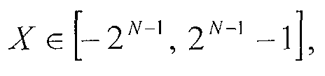
- the two's complement of -2 N -1 is represented with the positive integer 2 N -1 -1 generating at the same time an overflow flag OF signaling that the representation interval has been exceeded.
- a known two's complement circuit with overflow check is depicted in Figure 5. It generates an overflow flag OF when the string to be complemented represents the number -2 N -1 , and has a correction circuit CLIP that receives a two's complement string Z and the overflow flag OF, generating the correnct output string Y .
- the overflow check circuit OVERFLOW CHECK is input with the string X and with a string REF representing the number -2 N -1 , and activates the flag OF when the two strings coincide.
- the correction circuit CLIP generates an output string Y equal to the two's complement string Z when the flag OF is not active, while it produces the string 011...1 representing the number 2 N -1 -1 when the flag OF is active.
- the method of the invention contemplates the operations of generating an auxiliary string M of N bits in function of the string X, and of combining it logically with the string X to generate a corresponding output string Y .
- the least significant bit of the auxiliary string is independent from the bits of the string X, and any other bit M L , which is the ( L +1)-th least significant bit, of the auxiliary string is a logic combination of the L -th least significant bit M L -1 of the string M and of the L -th least significant bit X L -1 of the string X or of a negated replica thereof.
- an overflow flag OF is generated simply by combining logically the most significant bits M N -1 and X N -1 of the strings M and X. This is a great advantage because the overflow flag is generated by a single logic gate input with the bits M N -1 and X N -1 , independently from the number of bits N of the string X , while in known two's complement circuits it is generated by a N bit comparator that occupies a silicon area that is non negligible and depends on the length of the string X.
- the strings X and M are combined according to different logic operations for generating the output string Y .
- the method of the invention is implemented by a circuit for incrementing, decrementing or two's complementing a string constituted by a number N of bits, comprising
- Two equivalent embodiments of two's complement circuits implementing the method of the invention are depicted in Figures 6a and 6b, They have an auxiliary circuit OR MASK and AND MASK, respectively, input with the N -1 least significant bits of the string X and generating a corresponding auxiliary string M and M of N bits.
- the least significant bit X of the string X equal to 1
- the least significant bits of the auxiliary string from the second M 1 to the ( L +1)-th M L generated by the circuit of Figure 6a (or 6b) coincide with the L least significant bits of the string X (or with their negated replicas), while the remaining bits are all equal to 1 (or to 0), while the least significant bit of the auxiliary string M is independent from the string X and is 0 (or 1).
- FIG. 7a An auxiliary circuit OR MASK easy to realize is shown in Figure 7a. It is substantially composed of an array of OR gates in cascade, each gate being input with a bit of the string X and with the output of the OR gate that precedes in the cascade.
- FIG. 7b An auxiliary circuit AND MASK for the two's complement circuit of Figure 6b is depicted in Figure 7b. It is substantially similar to the circuit of Figure 7a but it has AND gates instead of OR gates and generates an auxiliary string M which is the negated replica of the auxiliary string M generated by the circuit of Figure 7a.
- the auxiliary circuit OR MASK (AND MASK) is substantially a circuit that generates a string M whose L least significant bits are equal to o (1) and all the remaining bits are equal to 1 (0), being X L-1 the least significant bit equal to 1 of the string X . Therefore, it is evident that the auxiliary circuit of Figure 7a (7b) may be substituted by any other circuit that carries out the same operation. For example, it is possible to substitute the circuit of Figure 7a, which has OR gates in series, with auxiliary circuits OR MASK of Figure 8a and 8b, that have OR gates disposed in parallel and in a hybrid series-parallel structure, respectively.
- the two's complement circuit of the invention may be used for realizing a circuit for decrementing, depicted in Figure 9a, a circuit for incrementing, depicted in Figure 10a, an increment/decrement circuit depicted in Figure 11a, or finally a multifunction DIT circuit, depicted in Figure 12a.
- Alternative embodiments of decrement, increment, increment/decrement and multifunction DIT circuits equivalent to those of Figures 9a, 10a, 11a and 12a are depicted in Figures 9b and 9c, in Figures 10b and 10c, in Figures from 11b to 11d and in Figures 12b and 12c, respectively.
- the method of the invention allows the generation of the overflow flag simply as logic combination only of the most significant bits M N -1 and X N -1 of the auxiliary string M and of the string to be complemented X , respectively, independently from the number N of bits of the string to be complemented.
- a two's complement circuit of the invention with overflow check is depicted in Figure 13.
- the circuit OVERFLOW CHECK can generate the overflow flag OF only using the most significant bits X N -1 and M N -1 because when the string X represents the number - 2 N -1 , and only in this case, the bit X N -1 is 1 and the bit M N -1 is 0.
- a great advantage of the present invention in respect to the known two's complement circuit of Figure 5 consists in the fact that the overflow flag OF is generated independently from the number N of bits of the string X, and the circuit OVERFLOW CHECK occupies surely a silicon area smaller than the area of a N bit comparator.
- FIG. 14 A detailed scheme of an embodiment of a two's complement circuit of the invention that performs the correction of eq. 6 is depicted in Figure 14.
- the XOR gate input with the bits X 0 and M 0 has been omitted because the least significant bit of the auxiliary string M 0 is always 0, and thus this gate is useless.
- the gate of the two's complement circuit input with the most significant bits M N -1 and X N -1 and generating the bit Z N -1 is an OR gate and not a XOR gate, in order to correct the output when the string X to be complemented represents the number -2 N -1 .
- the most significant bit YN -1 of the output string may be generated by negating the bit Z N -1 , as it is evident from the following table X M N -1 X N -1 Y N -1 Z N -1 0...0 0 0 0 1 -2 N -1 0 1 0 1 any other value 1 - X N- 1 X N -1
- the two's complement circuit with overflow test of Figure 13 may be used for realizing a multifunction DIT circuit of the invention for decrementing, incrementing and two's complementing, as depicted in Figure 15, whose circuit blocks are the same as that of Figures 4 and 13.
- Figure 17 depicts a general diagram of a preferred embodiment of a two's complement or decrement circuit of the invention.
- the correction circuit CLIP is upstream the array of output XOR gates and is not input with a bit string but only with two signals, INV_OUT and OF, whichever the number N of bits of the string K is.
- the correction circuit CLIP generates a correction signal INVCLIP and a negated replica of the signal INV_OUT, for making the array of output XOR gates perform the correction of eq. 6 of the complemented string Z . Therefore, the array of output XOR gates of the two's complement or decrement circuit of the invention is useful also when no decrement operation has been requested: this expedient allows a simplification of the structure of the correction circuit CLIP with a consequent further saving of silicon area.
- the two's complement or decrement circuit of the invention may be embodied in multifunction DIT circuit for incrementing, decrementing or two's complementing a string as shown in Figure 18.
- the truth table of signals INV_IN and INV_OUT is Table 1, already written referring to the multifunction DIT circuit of Figure 4.
- FIG. 19 A detailed scheme of an embodiment of the multifunction DIT circuit of Figure 18 is depicted in Figure 19.
- the overflow flag OF is generated by ANDing the most significant bit of the string to be two's complemented K N -1 and a negated replica of the most significant bit of the auxiliary string M N -1 , and the correction signal INVCLIP is the logic XOR between the overflow flag OF and the signal INV_OUT.
Landscapes
- Engineering & Computer Science (AREA)
- Physics & Mathematics (AREA)
- General Physics & Mathematics (AREA)
- Theoretical Computer Science (AREA)
- Computational Mathematics (AREA)
- Mathematical Analysis (AREA)
- Pure & Applied Mathematics (AREA)
- Computing Systems (AREA)
- Mathematical Optimization (AREA)
- General Engineering & Computer Science (AREA)
- Logic Circuits (AREA)
Abstract
Description


| ID | TC | | INV_IN | INV_OUT | |
| 0 | 0 | | 0 | 1 | |
| 1 | 0 | | 1 | 0 | |
| - | 1 | two | 0 | 0 |


- an auxiliary circuit generating an auxiliary string of N bits, in function of the first string, whose least significant bit is independent from the first string and any other bit, starting from the second least significant bit up to the most significant bit, is a logic combination of a corresponding bit of the first string or of a negated replica thereof, starting from the least significant bit up to the second most significant bit, and of the bits of the first string or of the negated replica thereof less significant than said corresponding bit;
- logic circuit means generating an output string as a logic combination of said auxiliary string and of said first string.
| X | M N-1 | X N-1 | Y N-1 | Z N-1 |
| 0...0 | 0 | 0 | 0 | 1 |
| -2 N-1 | 0 | 1 | 0 | 1 |
| any other value | 1 | - | | X N-1 |
Claims (38)
- A method for incrementing, decrementing or two's complementing a N bit string (K), comprising
generating an auxiliary string (M;M ) of N bits, in function of said string (K), whose least significant bit is independent from said string (K) and any other bit (MI ;MI ), starting from the second least significant bit (M l);M 1 ,) up to the most significant bit (M N-1;M N-1 ), is a logic combination of a corresponding bit (KI -1;KI -1 ) of said first string (K) or of a negated replica thereof (K ), starting from the least significant bit (K 0;K 0 ) up to the second most significant bit (KN -2;KN -2 ), and of the bits of said first string (K) or of the negated replica thereof (K ) less significant than said corresponding bit (K 0, ..., K I-2;K 0 , ...,K I-2 );
generating an output string (Y) as a logic combination of said auxiliary string (M;M ) and of said first string (K). - The method of claim 1, wherein
the least significant bit of said auxiliary string (M) is always null and any other bit (MI ), starting from the second least significant bit (M 1) up to the most significant bit (MN -1), is the logic OR of a corresponding bit of said first string (K I-1) or of a negated replica thereof (K I-1 ) and of said bits less significant than said corresponding bit (K 0, ..., K I-2;K 0 , ...,K I-2 ). - The method of claim 1, wherein
the least significant bit of said auxiliary string (M ) is always 1 and any other bit (MI ), starting from the second least significant bit (M 1 ) up to the most significant bit (M N-1 ), is the logic AND of a corresponding bit of said first string (KI-1) or of a negated replica thereof (K I-1 ) and of said bits less significant than said corresponding bit (K 0, ..., K I-2;K 0 , , ...,K I-2 ). - The method of claim 1, further comprising generating an overflow flag (OF) as a logic combination among the most significant bits of said auxiliary string (M N-1;
M N-1 ) and of said first string (K N-1). - The method of claim 2 for two's complementing said first string (K), wherein
said other bit of the auxiliary string (MI ) is obtained by ORing the immediately less significant bit (M I-1) of said auxiliary string (M) and a corresponding bit of said first string (K I-1);
said output string (Y) is obtained as XOR of said string (K) to be complemented and of said auxiliary string (M). - The method of claim 3 for two's complementing said first string (K), wherein
said other bit of the auxiliary string (MI ) is obtained by ANDing the immediately less significant bit (MI -1 ) of said auxiliary string (M ) and a corresponding bit of said first string (K I-1);
said output string (Y) is obtained as negated XOR of said string (K) to be complemented and of said auxiliary string (M ). - The method of claim 2 for decrementing said first string (K), wherein
said other bit of the auxiliary string (MI ) is obtained by ORing the immediately less significant bit (M I-1) of said auxiliary string (M) and a corresponding bit of said first string (K I-1);
said output string (Y) is obtained as negated XOR of said first string (K) and of said auxiliary string (M). - The method of claim 3 for decrementing said first string (K), wherein
said other bit of the auxiliary string (MI ) is obtained by ANDing the immediately less significant bit (M I-1 ) of said auxiliary string (M ) and a corresponding bit of said first string (K I-1);
said output string (Y) is obtained as XOR of said first string (K) and of said auxiliary string (M ). - The method of claim 2 for incrementing said first string (K), wherein
said other bit of the auxiliary string (MI ) is obtained by ORing the immediately less significant bit (M I-1) of said auxiliary string (M) and the negated replica (K I-1 ) of a corresponding bit of said first string (K I-1);
said output string (Y) is obtained by XORing said auxiliary string (M) and a negated replica of said first string (K). - The method of claim 3 for incrementing said first string (K), wherein
said other bit of the auxiliary string (MI ) is obtained by ANDing the immediately less significant bit (M I-1 ) of said auxiliary string (M ) and a corresponding bit of said first string (K I-1);
said output string (Y) is obtained as negated XOR of said first string (K) and of said auxiliary string (M ). - The method of claims 2 and 4 for two's complementing or decrementing said first string (K), wherein said overflow flag (OF) is generated by ANDing the most significant bit of said first string (K N-1) and a negated replica of the most significant bit of said auxiliary string (M N-1).
- The method of claims 3 and 4 for two's complementing or decrementing said first string (K), wherein said overflow flag (OF) is generated by ANDing the most significant bit of said first string (K N-1) and the most significant bit of said auxiliary string (
M N-1 ). - The method of claims 2 and 4 for incrementing said first string (K), wherein said overflow flag (OF) is generated by ANDing the negated replicas of the most significant bits of said first string (K N-1) and of said auxiliary string (MN -1).
- The method of claims 3 and 4 for incrementing said first string (K), wherein said overflow flag (OF) is generated by ANDing the negated replica of the most significant bit of said first string (K N-1) and the most significant bit of said auxiliary string (
M N-1 ). - The method of claim 11 for two's complementing said first string (K) with correction of the output in case of overflow, wherein
said other bit of the auxiliary string (MI ) is obtained by ORing the immediately less significant bit (M I-1) of said auxiliary string (M) and a corresponding bit of said string (K I-1);
the most significant bit of said output string (Y) is obtained by NORing the most significant bit of said first string (K N-1) and the negated replica of the most significant bit of said auxiliary string (M N-1),
any other bit of said output string (Y) is obtained by ORing the overflow flag (OF) and the logic XOR between corresponding bits of said first string (K) and of said auxiliary string (M). - The method of claim 11 for two's complementing said first string (K) with correction of the output in case of overflow, wherein
said other bit of the auxiliary string (MI ) is obtained by ORing the immediately less significant bit (M I-1) of said auxiliary string (M) and a corresponding bit of said string (K I-1);
the most significant bit of said output string (Y) is obtained by NORing the most significant bit of said first string (K N-1) and the negated replica of the most significant bit of said auxiliary string (M N-1),
any other bit of said output string (Y) is obtained by XORing the overflow flag (OF) and the logic XOR between corresponding bits of said first string (K) and of said auxiliary string (M). - The method of claim 11 for decrementing said first string (K) with correction of the output in case of overflow, wherein
said other bit of the auxiliary string (MI ) is obtained by ORing the immediately less significant bit (M I-1) of said auxiliary string (M) and a corresponding bit of said string (K I-1);
the most significant bit of said output string (Y) is obtained by ORing the most significant bit of said first string (K N-1) and the negated replica of the most significant bit of said auxiliary string (M N-1);
any other bit of said output string (Y) is obtained by XORing the negated replica of the overflow flag (OF) and the logic XOR between corresponding bits of said first string (K) and of said auxiliary string (M). - The method of claim 13 for incrementing said first string (K) with correction of the output in case of overflow, wherein
said other bit of the auxiliary string (MI ) is obtained by ORing the immediately less significant bit (MI -1) of said auxiliary string (M) and the negated replica (K I-1 ) of a corresponding bit of said string (K I-1);
the most significant bit of said output string (Y) is obtained by NORing the most significant bit of said first string (K N-1) and the negated replica of the most significant bit of said auxiliary string (M N-1);
any other bit of said output string (Y) is obtained by ORing the overflow flag (OF) and the logic XOR between corresponding bits of said first string (K) and of said auxiliary string (M). - A circuit for incrementing, decrementing or two's complementing a N bit string (K), comprising
an auxiliary circuit (OR MASK; AND MASK) generating an auxiliary string (M;M ) of N bits, in function of said string (K), whose least significant bit is independent from said string (K) and any other bit (MI ;MI ), starting from the second least significant bit (M 1;M 1 ) up to the most significant bit (M N-1;M N-1 ), is a logic combination of a corresponding bit (K I-1;K I-1 ) of said first string (K) or of a negated replica thereof (K ), starting from the least significant bit (K 0;K 0 ) up to the second most significant bit (K N-2;K N-2 ), and of the bits of said first string (K) or of the negated replica thereof (K ) less significant than said corresponding bit (K 0, ..., K I-2;K 0 , ...,K I-2 );
logic circuit means generating an output string (Y) as a logic combination of said auxiliary string (M;M ) and of said first string (K). - The circuit of claim 19, wherein said auxiliary circuit (OR MASK) generates the auxiliary string (M) with the least significant bit always null, the second least significant bit of said auxiliary string (M) as replica of the least significant bit of the first string (K 0) or as negated replica thereof (
K 0 ), and further comprises
N-2 OR gates each generating a respective bit of said auxiliary string (M), starting from the third least significant bit (M 2) up to the most significant bit (M N-1) by ORing a corresponding bit (K I-1;K I-1) of said first string (K) or of a negated replica thereof (K ), starting from the least significant bit (K 0;K 0 ) up to the second most significant bit (K N-2;K N-2 ), and the bits of said first string (K) or of the negated replica thereof (K ) less significant than said corresponding bit (K 0, ..., K I-2; K 0 , ...,K I-2 ). - The circuit of claim 19, wherein said auxiliary circuit (OR MASK) generates the auxiliary string (M) with the least significant bit always null, the second least significant bit of said auxiliary string (M) as replica of the least significant bit of the first string (K 0) or as negated replica thereof (
K 0), and further comprises
N-2 OR gates each generating a respective bit of said auxiliary string (M), starting from the third least significant bit (M 2) up to the most significant bit (M N-1), disposed in a cascade of pairs of logic gates, the gates of a first pair generating the third and fourth least significant bits of said auxiliary string (M 2, M 3) by ORing the two (K 0, K 1) and the three least significant bits (K 0, K 1, K 2), respectively, of said first string (K) or of the negated replica thereof (K ), each pair of OR gates being input with a respective pair of consecutive bits first (K I-2) and second (K I-1) of said first string (K) or of the negated replica thereof (K ) and the most significant bit of said auxiliary string generated by the pair of gates that precedes in the cascade (M I-2), and generating two consecutive bits of said auxiliary string (M I-1, MI ) by ORing said most significant bit generated by the pair of gates that precedes in the cascade (M I-2) and respectively said first bit (K I-2) and both said bits first (K I-2) and second (K I-1) of said respective pair of bits. - The circuit of claim 19, wherein said auxiliary circuit (OR MASK) generates the auxiliary string (M) with the least significant bit always null, the second least significant bit of said auxiliary string (M) as replica of the least significant bit of the first string (K 0) or as negated replica thereof (
K 0) , and further comprises
a cascade of N-2 OR gates input with a respective bit of said first string (K) or of the negated replica thereof in order starting from the second least significant bit (K 1) up to the second most significant bit (K N-2), each gate generating a respective bit of said auxiliary string (M), starting from the third least significant bit (M 2) up to the most significant bit (M N-1), as logic OR of the respective bit of said first string (K) or of the negated replica thereof and of the bit of the auxiliary string (M) generated by the OR gate that precedes in the cascade. - The circuit of claim 19, wherein said auxiliary circuit (AND MASK) generates the auxiliary string (
M ) with the least significant bit always equal to 1, the second least significant bit of said auxiliary string (M ) as replica of the least significant bit of the first string (K 0) or as negated replica thereof (K 0 ), and further comprises
a cascade of N-2 AND gates input with a respective bit of said first string (K) or of the negated replica thereof in order starting from the second least significant bit (K 1) up to the second most significant bit (K N-2), each gate generating a respective bit of said auxiliary string (M ), starting from the third least significant bit (M 2 ) up to the most significant bit (M N-1 ), by ANDing the respective bit of said first string (K) or of a negated replica thereof and the bit of the auxiliary string (M ) generated by the AND gate that precedes in the cascade. - The circuit of claim 19, comprising an overflow control circuit (OVERFLOW CHECK) generating an overflow flag (OF) as logic combination among the most significant bits of said auxiliary string (M N-1;
M N-1 ) and of said first string (K N-1). - The circuit of claim 22 for two's complementing said first string (K), wherein
each of said bits of the auxiliary string (M I ) starting from the third least significant bit (M 2) are obtained by ORing the immediately less significant bit (M I-1) of said auxiliary string (M) and a corresponding bit of said string (K I-1);
said logic circuit means comprise an array of XOR gates, generating bits of said output string (Y) by XORing respective bits of said string to be complemented (K) and of said auxiliary string (M). - The circuit of claim 22 for decrementing said first string (K), wherein
each of said bits of the auxiliary string (M I ) starting from the third least significant bit (M 2) are obtained by ORing the immediately less significant bit (M I-1) of said auxiliary string (M) and a corresponding bit of said string (K I-1);
said logic circuit means comprise an array of XOR gates, generating bits of a two's complement string (Z) by XORing respective bits of said string to be complemented (K) and of said auxiliary string (M), and an array of NOT gates each input with a bit of the two's complement string and generating a corresponding bit of said output string (Y). - The circuit of claim 22 for incrementing said first string (K), wherein
each of said bits of the auxiliary string (M I ) starting from the third least significant bit (M 2) are obtained by ORing the immediately less significant bit (M I-1) of said auxiliary string (M) and the negated replica (K I-1 ) of a corresponding bit of said string (K I-1);
said logic circuit means comprise an array of XOR gates, generating bits of said output string (Y) by XORing respective bits of said string to be complemented (K) and of said auxiliary string (M). - The circuit of claims 20 and 24 for two's complementing or decrementing said first string (K), wherein said overflow check circuit (OVERFLOW CHECK) is a logic AND gate generating said overflow flag (OF), input with the most significant bit of said first string (K N-1) and a negated replica of the most significant bit of said auxiliary string (M N-1).
- The circuit of claims 23 and 24 for two's complementing or decrementing said first string (K), wherein said overflow check circuit (OVERFLOW CHECK) is a logic AND gate generating said overflow flag (OF), input with the most significant bits of said first string (K N-1) and of said auxiliary string (
M N-1 ). - The circuit of claims 20 and 24 for incrementing said first string (K), wherein said overflow check circuit (OVERFLOW CHECK) is a logic AND gate generating said overflow flag (OF), input with the negated replicas of the most significant bits of said first string (K N-1) and of said auxiliary string (M N-1).
- The circuit of claims 23 and 24 for incrementing said first string (K), wherein said overflow check circuit (OVERFLOW CHECK) is a logic AND gate generating said overflow flag (OF), input with a negated replica of the most significant bit of said first string (K N-1) and the most significant bit of said auxiliary string (
M N-1 ). - The circuit of claim 22 for incrementing or decrementing an input string (X) constituted by a number N of bits, comprising
an input terminal for receiving a command signal (ID) of the operation to be performed;
an array of N XOR gates each input with a respective bit of said input string (X) and with said command signal (ID) generating a corresponding bit of said first string (K);
each of said bits of the auxiliary string (MI ) starting from the third least significant bit (M 2) are generated by ORing the immediately less significant bit (MI -1) of said auxiliary string (M) and a corresponding bit of said string (K I-1);
said circuit logic means comprising an array of logic gates generating bits of said output string (Y) by XORing a negated replica of said selection command (ID) and the logic XOR of respective bits of said input string (X) and of said auxiliary string (M). - The circuit of claim 22, comprising
a logic selection circuit (SEL) input with command signals (ID, TC) identifying the operation to be performed and generating a pair of selection signals first (INV_OUT) and second (INV_IN) whose logic state depends on the operation to be carried out,
an array of N input XOR gates each input with a respective bit of said input string (X) and said second selection signal (INV_IN), generating said first bit string (K),
each of said bits of the auxiliary string (MI ) starting from the third least significant bit (M 2) are obtained by ORing the immediately less significant bit (M I-1) of said auxiliary string (M) and a corresponding bit of said string (KI -1);
said logic circuit means comprising an array of logic gates generating bits of said output string (Y) by XORing said first selection signal (INV_OUT) and the logic XOR of respective bits of said input string (X) and of said auxiliary string (M). - The circuit of claim 28 for two's complementing with correction of the output in case of overflow, wherein each of said bits of the auxiliary string (M I ) starting from the third least significant bit (M 2) are obtained by ORing the immediately less significant bit (M I-1) of said auxiliary string (M) and a corresponding bit of said string (K I-1);
said logic circuit means comprise
an OR gate input with the most significant bit of said first string (K N-1) and the negated replica of the most significant bit of said auxiliary string (M N-1), generating the most significant bit of a two's complement string to be corrected (Z N-1),
an array of XOR gates generating the other bits of said two's complement string to be corrected (Z) by XORing corresponding bits of said first string (K) and of said auxiliary string (M);
a correction circuit (CLIP) having
a NOT gate generating the most significant bit of said output string (Y N-1) as negated replica of the most significant bit of said two's complement string to be corrected (Z N-1),
an array of N-1 OR gates generating respective other bits of said output string (Y), each gate being input with said overflow flag (OF) and with an output of a respective gate XOR of said array. - The circuit of claim 28 for two's complementing or decrementing with correction of the output in case of overflow, having an input terminal receiving a selection signal (INV_OUT) of the operation to be performed, wherein
each of said bits of the auxiliary string (MI ) starting from the third least significant bit (M 2) are obtained by ORing the immediately less significant bit (M I-1) of said auxiliary string (M) and of a corresponding bit of said string (K I-1);
said logic circuit means comprise
an OR gate input with the most significant bit of said first string (K N-1) and the negated replica of the most significant bit of said auxiliary string (M N-1), generating the most significant bit of a two's complement string to be corrected (Z N-1),
an array of XOR gates generating the other bits of said two's complement string to be corrected (Z) by XORing corresponding bits of said first string (K) and of said auxiliary string (M);
an output logic circuit input with said two's complement string (Z), said overflow flag (OF) and said selection signal and said selection signal (INV_OUT), generating an output bit string (Y) equal to said two's complement string (Z) or obtained by negating all the bits thereof depending on the logic state of said selection signal (INV_OUT) and of said overflow flag (OF). - The circuit of claim 35 for two's complementing or decrementing with correction of the output in case of overflow, wherein said output logic circuit comprises
a logic correction circuit (CLIP) generating a negated replica of said selection signal (INV_OUT ) and a correction signal (INVCLIP) by XORing said selection signal (INV_OUT) and said overflow flag (OF);
an array of N logic XOR gates, one of them being input with the most significant bit (Z N-1) of said two's complement bit string (Z) and with said negated replica (INV_OUT ) generating the most significant bit of the output string (Y N-1), and each other XOR gate being input with a respective other bit of said two's complement string (Z) and said correction signal (INVCLIP) generating corresponding other bits of the output string (Y). - A multifunction circuit (DIT) for decrementing, incrementing or two's complementing an input N bit string (X), comprising
a logic selection circuit (SEL) input with command signals (ID, TC) identifying the operation to be performed and generating a pair of selection signals first (INV_OUT) and second (INV_IN) whose logic state depends on the operation to be performed,
an array of N XOR input gates each input with a respective bit of said input string (X) and with said first logic signal (INV_IN), generating said first bit string (K),
a circuit for two's complementing or decrementing as defined in claim 35, input with said first bit string (K) and generating said output bit string (Y). - The multifunction circuit (DIT) of claim 37, wherein said selection circuit (SEL) is input with a pair of command signals first (ID) and second (TC) and generatessaid first logic signal (INV_OUT) by NORing said command signals (ID, TC);said second logic signal (INV_IN) by ANDing said first command signal (ID) and a negated replica of said second command signal (TC).
Priority Applications (2)
| Application Number | Priority Date | Filing Date | Title |
|---|---|---|---|
| EP02425538A EP1394673A1 (en) | 2002-08-30 | 2002-08-30 | Method and circuit for incrementing, decrementing or two complementing a bit string |
| US10/651,075 US7395305B2 (en) | 2002-08-30 | 2003-08-28 | Method and relative circuit for incrementing, decrementing or two's complementing a bit string |
Applications Claiming Priority (1)
| Application Number | Priority Date | Filing Date | Title |
|---|---|---|---|
| EP02425538A EP1394673A1 (en) | 2002-08-30 | 2002-08-30 | Method and circuit for incrementing, decrementing or two complementing a bit string |
Publications (1)
| Publication Number | Publication Date |
|---|---|
| EP1394673A1 true EP1394673A1 (en) | 2004-03-03 |
Family
ID=31198025
Family Applications (1)
| Application Number | Title | Priority Date | Filing Date |
|---|---|---|---|
| EP02425538A Withdrawn EP1394673A1 (en) | 2002-08-30 | 2002-08-30 | Method and circuit for incrementing, decrementing or two complementing a bit string |
Country Status (2)
| Country | Link |
|---|---|
| US (1) | US7395305B2 (en) |
| EP (1) | EP1394673A1 (en) |
Cited By (1)
| Publication number | Priority date | Publication date | Assignee | Title |
|---|---|---|---|---|
| WO2009158254A1 (en) * | 2008-06-26 | 2009-12-30 | Qualcomm Incorporated | System and method to perform fast rotation operations |
Families Citing this family (1)
| Publication number | Priority date | Publication date | Assignee | Title |
|---|---|---|---|---|
| US20230195417A1 (en) * | 2021-12-22 | 2023-06-22 | Intel Corporation | Parallel computation of a logic operation, increment, and decrement of any portion of a sum |
Citations (3)
| Publication number | Priority date | Publication date | Assignee | Title |
|---|---|---|---|---|
| US4534010A (en) * | 1980-10-31 | 1985-08-06 | Hitachi, Ltd. | Floating point type multiplier circuit with compensation for over-flow and under-flow in multiplication of numbers in two's compliment representation |
| US5146479A (en) * | 1990-06-05 | 1992-09-08 | Mitsubishi Denki Kabushiki Kaisha | Up/down counter for counting binary data stored in flip flops |
| US5333120A (en) * | 1992-11-17 | 1994-07-26 | Gilber T Joseph R | Binary two's complement arithmetic circuit |
Family Cites Families (7)
| Publication number | Priority date | Publication date | Assignee | Title |
|---|---|---|---|---|
| US3532866A (en) * | 1966-11-30 | 1970-10-06 | Nasa | Ripple add and ripple subtract binary counters |
| JPS537349B2 (en) * | 1974-03-27 | 1978-03-16 | ||
| US4153939A (en) * | 1976-01-24 | 1979-05-08 | Nippon Electric Co., Ltd. | Incrementer circuit |
| US4218750A (en) * | 1978-09-25 | 1980-08-19 | Motorola, Inc. | Incrementer with common precharge enable and carry-in signal |
| US4417316A (en) * | 1981-07-14 | 1983-11-22 | Rockwell International Corporation | Digital binary increment circuit apparatus |
| US4486851A (en) * | 1982-07-01 | 1984-12-04 | Rca Corporation | Incrementing/decrementing circuit as for a FIR filter |
| JPH01204138A (en) * | 1988-02-09 | 1989-08-16 | Nec Corp | Arithmetic circuit |
-
2002
- 2002-08-30 EP EP02425538A patent/EP1394673A1/en not_active Withdrawn
-
2003
- 2003-08-28 US US10/651,075 patent/US7395305B2/en not_active Expired - Fee Related
Patent Citations (3)
| Publication number | Priority date | Publication date | Assignee | Title |
|---|---|---|---|---|
| US4534010A (en) * | 1980-10-31 | 1985-08-06 | Hitachi, Ltd. | Floating point type multiplier circuit with compensation for over-flow and under-flow in multiplication of numbers in two's compliment representation |
| US5146479A (en) * | 1990-06-05 | 1992-09-08 | Mitsubishi Denki Kabushiki Kaisha | Up/down counter for counting binary data stored in flip flops |
| US5333120A (en) * | 1992-11-17 | 1994-07-26 | Gilber T Joseph R | Binary two's complement arithmetic circuit |
Non-Patent Citations (4)
| Title |
|---|
| B. PARHAMI: "COMPUTER ARITHMETIC: ALGORITHMS AND HARDWARE DESIGNS", 2000, OXFORD UNIVERSITY PRESS, NEW YORK, ISBN: 0-19-512583-5, XP002245799, 239790 * |
| HASHEMIAN R ET AL: "A NEW PARALLEL TECHNIQUE FOR DESIGN OF DECREMENT/INCREMENT AND TWO'S COMPLEMENT CIRCUITS", PROCEEDINGS OF THE MIDWEST SYMPOSIUM ON CIRCUITS AND SYSTEMS. MONTEREY, MAY 14 - 17, 1991, NEW YORK, IEEE, US, vol. 2 SYMP. 34, 14 May 1991 (1991-05-14), pages 887 - 890, XP000333546 * |
| KAZUYA SONE ET AL: "A 10-B 100-MSAMPLE/S PIPELINED SUBRANGING BICMOS ADC", IEEE JOURNAL OF SOLID-STATE CIRCUITS, IEEE INC. NEW YORK, US, vol. 28, no. 12, 1 December 1993 (1993-12-01), pages 1180 - 1186, XP000435890, ISSN: 0018-9200 * |
| STAN M R: "SYNCHRONOUS UP/DOWN COUNTER WITH CLOCK PERIOD INDEPENDENT OF COUNTER SIZE", PROCEEDINGS 13TH IEEE SYMPOSIUM ON COMPUTER ARITHMETIC. ASILOMAR, CA, JULY 6 - 9, 1997, IEEE SYMPOSIUM ON COMPUTER ARITHMETIC, LOS ALAMITOS, CA: IEEE COMP. SOC. PRESS, US, 6 July 1997 (1997-07-06), pages 274 - 281, XP000788135, ISBN: 0-8186-7846-1 * |
Cited By (6)
| Publication number | Priority date | Publication date | Assignee | Title |
|---|---|---|---|---|
| WO2009158254A1 (en) * | 2008-06-26 | 2009-12-30 | Qualcomm Incorporated | System and method to perform fast rotation operations |
| CN102067082A (en) * | 2008-06-26 | 2011-05-18 | 高通股份有限公司 | System and method to perform fast rotation operations |
| JP2011526041A (en) * | 2008-06-26 | 2011-09-29 | クゥアルコム・インコーポレイテッド | System and method for performing high-speed rotation calculation |
| US8243100B2 (en) | 2008-06-26 | 2012-08-14 | Qualcomm Incorporated | System and method to perform fast rotation operations |
| KR101334860B1 (en) * | 2008-06-26 | 2013-12-02 | 퀄컴 인코포레이티드 | System and method to perform fast rotation operations |
| CN102067082B (en) * | 2008-06-26 | 2014-07-09 | 高通股份有限公司 | System and method to perform fast rotation operations |
Also Published As
| Publication number | Publication date |
|---|---|
| US20040073586A1 (en) | 2004-04-15 |
| US7395305B2 (en) | 2008-07-01 |
Similar Documents
| Publication | Publication Date | Title |
|---|---|---|
| US20020165886A1 (en) | Modification to reconfigurable functional unit in a reconfigurable chip to perform linear feedback shift register function | |
| US8495116B2 (en) | Circuit and method converting boolean and arithmetic masks | |
| US5027310A (en) | Carry chain incrementer and/or decrementer circuit | |
| US5774080A (en) | Reduced transistor-count data storage and multiplexing system | |
| US7360148B2 (en) | Reduction checksum generator and a method of calculation thereof | |
| US6055557A (en) | Adder circuit and method therefor | |
| US7395305B2 (en) | Method and relative circuit for incrementing, decrementing or two's complementing a bit string | |
| US6434588B1 (en) | Binary counter with low power consumption | |
| JPH0379736B2 (en) | ||
| US20020188641A1 (en) | Logic circuit for fast carry/borrow | |
| US5588010A (en) | Parallel architecture error correction and conversion system | |
| US6738792B1 (en) | Parallel mask generator | |
| US6341327B1 (en) | Content addressable memory addressable by redundant form input | |
| US4879675A (en) | Parity generator circuit and method | |
| US6489811B2 (en) | Logic gate with symmetrical propagation delay from any input to any output and a controlled output pulse width | |
| US5977864A (en) | High speed comparator with bit-wise masking | |
| US6782467B1 (en) | Method and apparatus for fast limited core area access and cross-port word size multiplication in synchronous multiport memories | |
| RU2143722C1 (en) | Device for multiplication by modulo 7 | |
| US7085796B1 (en) | Dynamic adder with reduced logic | |
| US20020018539A1 (en) | Multi-bit counter | |
| SU1203693A1 (en) | Threshold element | |
| RU2107953C1 (en) | Device for writing and reading multiple- channel digital information | |
| US6581084B1 (en) | Circuit for multiplication in a Galois field | |
| EP1081590B1 (en) | An incrementer/decrementer having a reduced fan-out architecture | |
| RU2149442C1 (en) | Device for modulo seven multiplication |
Legal Events
| Date | Code | Title | Description |
|---|---|---|---|
| PUAI | Public reference made under article 153(3) epc to a published international application that has entered the european phase |
Free format text: ORIGINAL CODE: 0009012 |
|
| AK | Designated contracting states |
Kind code of ref document: A1 Designated state(s): AT BE BG CH CY CZ DE DK EE ES FI FR GB GR IE IT LI LU MC NL PT SE SK TR |
|
| AX | Request for extension of the european patent |
Extension state: AL LT LV MK RO SI |
|
| 17P | Request for examination filed |
Effective date: 20040809 |
|
| AKX | Designation fees paid |
Designated state(s): DE FR GB IT |
|
| 17Q | First examination report despatched |
Effective date: 20050112 |
|
| APBN | Date of receipt of notice of appeal recorded |
Free format text: ORIGINAL CODE: EPIDOSNNOA2E |
|
| APBR | Date of receipt of statement of grounds of appeal recorded |
Free format text: ORIGINAL CODE: EPIDOSNNOA3E |
|
| APAF | Appeal reference modified |
Free format text: ORIGINAL CODE: EPIDOSCREFNE |
|
| RAP1 | Party data changed (applicant data changed or rights of an application transferred) |
Owner name: STMICROELECTRONICS SRL |
|
| APAF | Appeal reference modified |
Free format text: ORIGINAL CODE: EPIDOSCREFNE |
|
| APBT | Appeal procedure closed |
Free format text: ORIGINAL CODE: EPIDOSNNOA9E |
|
| STAA | Information on the status of an ep patent application or granted ep patent |
Free format text: STATUS: THE APPLICATION HAS BEEN WITHDRAWN |
|
| 18W | Application withdrawn |
Effective date: 20111014 |