EP1392049A2 - Image forming apparatus - Google Patents
Image forming apparatus Download PDFInfo
- Publication number
- EP1392049A2 EP1392049A2 EP03018999A EP03018999A EP1392049A2 EP 1392049 A2 EP1392049 A2 EP 1392049A2 EP 03018999 A EP03018999 A EP 03018999A EP 03018999 A EP03018999 A EP 03018999A EP 1392049 A2 EP1392049 A2 EP 1392049A2
- Authority
- EP
- European Patent Office
- Prior art keywords
- signal
- image
- pseudo
- forming apparatus
- image forming
- Prior art date
- Legal status (The legal status is an assumption and is not a legal conclusion. Google has not performed a legal analysis and makes no representation as to the accuracy of the status listed.)
- Granted
Links
Images







Classifications
-
- G—PHYSICS
- G03—PHOTOGRAPHY; CINEMATOGRAPHY; ANALOGOUS TECHNIQUES USING WAVES OTHER THAN OPTICAL WAVES; ELECTROGRAPHY; HOLOGRAPHY
- G03G—ELECTROGRAPHY; ELECTROPHOTOGRAPHY; MAGNETOGRAPHY
- G03G15/00—Apparatus for electrographic processes using a charge pattern
-
- H—ELECTRICITY
- H04—ELECTRIC COMMUNICATION TECHNIQUE
- H04N—PICTORIAL COMMUNICATION, e.g. TELEVISION
- H04N1/00—Scanning, transmission or reproduction of documents or the like, e.g. facsimile transmission; Details thereof
- H04N1/46—Colour picture communication systems
- H04N1/50—Picture reproducers
- H04N1/506—Reproducing the colour component signals picture-sequentially, e.g. with reproducing heads spaced apart from one another in the subscanning direction
-
- H—ELECTRICITY
- H04—ELECTRIC COMMUNICATION TECHNIQUE
- H04N—PICTORIAL COMMUNICATION, e.g. TELEVISION
- H04N1/00—Scanning, transmission or reproduction of documents or the like, e.g. facsimile transmission; Details thereof
- H04N1/04—Scanning arrangements, i.e. arrangements for the displacement of active reading or reproducing elements relative to the original or reproducing medium, or vice versa
- H04N1/047—Detection, control or error compensation of scanning velocity or position
- H04N1/053—Detection, control or error compensation of scanning velocity or position in main scanning direction, e.g. synchronisation of line start or picture elements in a line
-
- H—ELECTRICITY
- H04—ELECTRIC COMMUNICATION TECHNIQUE
- H04N—PICTORIAL COMMUNICATION, e.g. TELEVISION
- H04N1/00—Scanning, transmission or reproduction of documents or the like, e.g. facsimile transmission; Details thereof
- H04N1/04—Scanning arrangements, i.e. arrangements for the displacement of active reading or reproducing elements relative to the original or reproducing medium, or vice versa
- H04N1/06—Scanning arrangements, i.e. arrangements for the displacement of active reading or reproducing elements relative to the original or reproducing medium, or vice versa using cylindrical picture-bearing surfaces, i.e. scanning a main-scanning line substantially perpendicular to the axis and lying in a curved cylindrical surface
-
- H—ELECTRICITY
- H04—ELECTRIC COMMUNICATION TECHNIQUE
- H04N—PICTORIAL COMMUNICATION, e.g. TELEVISION
- H04N1/00—Scanning, transmission or reproduction of documents or the like, e.g. facsimile transmission; Details thereof
- H04N1/04—Scanning arrangements, i.e. arrangements for the displacement of active reading or reproducing elements relative to the original or reproducing medium, or vice versa
- H04N1/113—Scanning arrangements, i.e. arrangements for the displacement of active reading or reproducing elements relative to the original or reproducing medium, or vice versa using oscillating or rotating mirrors
- H04N1/1135—Scanning arrangements, i.e. arrangements for the displacement of active reading or reproducing elements relative to the original or reproducing medium, or vice versa using oscillating or rotating mirrors for the main-scan only
-
- H—ELECTRICITY
- H04—ELECTRIC COMMUNICATION TECHNIQUE
- H04N—PICTORIAL COMMUNICATION, e.g. TELEVISION
- H04N2201/00—Indexing scheme relating to scanning, transmission or reproduction of documents or the like, and to details thereof
- H04N2201/04—Scanning arrangements
- H04N2201/047—Detection, control or error compensation of scanning velocity or position
- H04N2201/04701—Detection of scanning velocity or position
- H04N2201/0471—Detection of scanning velocity or position using dedicated detectors
-
- H—ELECTRICITY
- H04—ELECTRIC COMMUNICATION TECHNIQUE
- H04N—PICTORIAL COMMUNICATION, e.g. TELEVISION
- H04N2201/00—Indexing scheme relating to scanning, transmission or reproduction of documents or the like, and to details thereof
- H04N2201/04—Scanning arrangements
- H04N2201/047—Detection, control or error compensation of scanning velocity or position
- H04N2201/04701—Detection of scanning velocity or position
- H04N2201/04732—Detecting at infrequent intervals, e.g. once or twice per line for main-scan control
-
- H—ELECTRICITY
- H04—ELECTRIC COMMUNICATION TECHNIQUE
- H04N—PICTORIAL COMMUNICATION, e.g. TELEVISION
- H04N2201/00—Indexing scheme relating to scanning, transmission or reproduction of documents or the like, and to details thereof
- H04N2201/04—Scanning arrangements
- H04N2201/047—Detection, control or error compensation of scanning velocity or position
- H04N2201/04701—Detection of scanning velocity or position
- H04N2201/04744—Detection of scanning velocity or position by detecting the scanned beam or a reference beam
-
- H—ELECTRICITY
- H04—ELECTRIC COMMUNICATION TECHNIQUE
- H04N—PICTORIAL COMMUNICATION, e.g. TELEVISION
- H04N2201/00—Indexing scheme relating to scanning, transmission or reproduction of documents or the like, and to details thereof
- H04N2201/04—Scanning arrangements
- H04N2201/047—Detection, control or error compensation of scanning velocity or position
- H04N2201/04753—Control or error compensation of scanning position or velocity
- H04N2201/04758—Control or error compensation of scanning position or velocity by controlling the position of the scanned image area
- H04N2201/04767—Control or error compensation of scanning position or velocity by controlling the position of the scanned image area by controlling the timing of the signals, e.g. by controlling the frequency o phase of the pixel clock
- H04N2201/04781—Controlling the phase of the signals
- H04N2201/04786—Controlling a start time, e.g. for output of a line of data
-
- H—ELECTRICITY
- H04—ELECTRIC COMMUNICATION TECHNIQUE
- H04N—PICTORIAL COMMUNICATION, e.g. TELEVISION
- H04N2201/00—Indexing scheme relating to scanning, transmission or reproduction of documents or the like, and to details thereof
- H04N2201/04—Scanning arrangements
- H04N2201/047—Detection, control or error compensation of scanning velocity or position
- H04N2201/04753—Control or error compensation of scanning position or velocity
- H04N2201/04793—Control or error compensation of scanning position or velocity using stored control or compensation data, e.g. previously measured data
Definitions
- This invention relates to an image forming apparatus using an electrophotographic process, and particularly to a color image forming apparatus for forming different color images by the use of a plurality of laser beams.
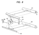
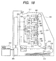
- the image forming portions comprise toner cartridges 207 to 210 having photosensitive drums 301-304 as image bearing members, and scanner units 205 and 206 having laser diodes (corresponding to laser beam generating elements in the appended claims) for generating laser beams as image exposing light sources.
- a toner cartridge is provided for each of the four colors.
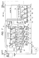
- the video controller transmits the video signal to the engine controller a predetermined time after it has detected the output signal of the BD sensor 106. Thereby, the writing-out positions for the main scanning of the images on the photosensitive drums by the laser beam always coincide with one another.
- the BD sensor is not present on the scanning path of the laser diode 102 and therefore, a BD signal for the laser diode LD2 is produced by the engine controller 204.
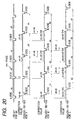
- a horizontal synchronizing signal on the laser side not having this BD sensor will be called a pseudo /BD signal. The details of a producing method will be describe later.
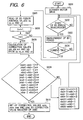
- the CPU 403 instructs the ASIC 402 to start the measurement of the BD period (S602).
- the ASIC 402 measures the BD period of each side of the polygon (S603), and the average values of the BD periods of the respective sides of the polygon are calculated.
- the ASIC 402 outputs the BD period measurement terminating bit poriend to the CPU 403.
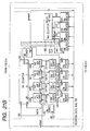
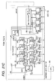
- the side division error of the polygon can be eliminated by measuring the BD period of each side of the polygon, and producing from the BD period the BD signal (pseudo BD signal) of the side without the BD sensor.
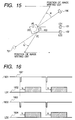
- the pseudo /BD signal side for black (BK) is using the D side
- the pseudo /BD signal side for yellow (Y) uses the A side
- the pseudo /BD signal side for magenta (M) uses the B side
- the pseudo /BD signal side for cyan (C) uses the C side
- the correction values are determined from such correspondence between the /BD signal side and the pseudo /BD signal side.
- the correction value of the pseudo /BD signal 1903 for yellow (Y) of the /BD signal 401 of the C side is xc-xb and therefore, a pseudo /BD signal 1903 for yellow delayed by (xc-xb) clocks form the /BD signal 401 is produced and outputted.
Landscapes
- Engineering & Computer Science (AREA)
- Multimedia (AREA)
- Signal Processing (AREA)
- Physics & Mathematics (AREA)
- General Physics & Mathematics (AREA)
- Facsimile Scanning Arrangements (AREA)
- Color Electrophotography (AREA)
- Laser Beam Printer (AREA)
- Control Or Security For Electrophotography (AREA)
- Mechanical Optical Scanning Systems (AREA)
- Exposure Or Original Feeding In Electrophotography (AREA)
- Fax Reproducing Arrangements (AREA)
Abstract
To this end, The image forming apparatus is provided with a plurality of image bearing members, an optical system having a plurality of light emitting elements suitable for generating light beams for scanning the image bearing members, a single polygon mirror suitable for deflecting the light beams generated from the plurality of light emitting elements onto the image bearing members, and a beam detector corresponding to at least one of the plurality of image bearing members, and for receiving the light beams scanned by the polygon mirror and producing a first synchronizing signal for recording an image on the relevant image bearing member, a storing portion suitable for storing therein information regarding the error of each side of the polygon mirror, and a producing unit suitable for producing a second synchronizing signal for recording an image on the image bearing member not provided with the beam detector, by delaying the first synchronizing signal outputted from the beam detector, on the basis of the value of the storing portion.
Description
the correction value of the B side of the pseudo /BD signal corresponding to the A side of the /BD signal side is
(the period of the A side of the BD signal) - (the shortest BD period)
= xa-xb,
the correction value is xa-xb;
the correction value of the C side of the pseudo /BD signal corresponding to the B side of the /BD signal side is
(the period of the B side of the BD signal) - (the shortest BD period)
= xb-xb,
the correction value is 0;
the correction value of the D side of the pseudo /BD signal corresponding to the C side of the /BD signal side is
(the period of the C side of the BD signal) - (the shortest BD period)
= xc-xb,
the correction value is xc-xb;
the correction value of the A side of the pseudo /BD signal corresponding to the D side of the /BD signal side is
(the period of the D side of the BD signal) - (the shortest BD period)
= xd-xa,
the correction value is xd-xa.
the correction value of the C side of the pseudo /BD signal corresponding to the A side of the /BD signal side is
(the combined period of the A side and the B side of the /BD signal)-(the shortest BD period)
=xa_b-xa_b,
the correction value is 0;
the correction value of the D side of the pseudo /BD signal corresponding to the B side of the BD signal side is
(the combined period of the B side and the C side of the BD signal)-(the shortest BD period) =xb_c-xa_b,
the correction value is xb_c-xa_b;
the correction value of the A side of the pseudo /BD signal corresponding to the C side of the /BD signal side is
(the combined period of the C side and the D side of the /BD signal)-(the shortest BD period)
=xc_d-xa_b,
the correction value is xc_d-xa_b;
the correction value of the B side of the pseudo /BD signal corresponding to the D side of the /BD signal side is
(the combined period of the D side and the A side of the /BD signal)-(the shortest BD period)
=xd_a-xa_b,
the correction value is xd_a-xa_b.
and the correction values are determined from such correspondence between the /BD signal side and the pseudo /BD signal side.
the correction value of the B side of the pseudo /
(the period of the A side of the BD signal)-(the shortest BD period)
=xa-xb,
the correction value is xa-xb;
the correction value of the C side of the pseudo /
(the period of the B side of the BD signal)-
(the shortest BD period)
=xb-xb,
the correction value is 0;
the correction value of the D side of the pseudo /
(the period of the C side of the BD signal)-
(the shortest BD period)
=xc-xb,
the correction value is xc-xb;
the correction value of the A side of the pseudo /
(the period of the D side of the BD signal)-
(the shortest BD period)
=xd-xa,
the correction value is xd-xa.
the correction value of the A side of the /
xa-xb and therefore,
the correction value of the C side of the pseudo /
0+xa-xb
=xa-xb.
xc-xb, and
the correction value of the B side of the /
the correction value of the D side of the pseudo /
xc-
=xc-xb.
the correction value of the C side of the /
the correction value of the A side of the pseudo /
xc-xb+xd-xb
=xc+xd-2xb.
the correction value of the D side of the /
the correction value of the B side of the pseudo /
xa-xb+xd-xb
=xa+xd-2xb.
the correction value of the A side of the /
xa-xb and therefore,
the correction value of the D side of the pseudo /
xc-xb+xa-xb
=xa+xc-2xb.
xd-xb, and
the correction value of the B side of the /
the correction value of the A side of the pseudo /
xd-xb+xc-xb
=xc+xd-2xb.
the correction value of the C side of the /
xc+xd-2xb and therefore,
the correction value of the B side of the pseudo /
xa-xb+xc+xd-2xb
=xa+xc+xd-3xb.
and the correction value of the D side of the /
xa+xd-2xb and therefore,
the correction value of the C side of the pseudo /
0+xa+xd-2xb
=xa+xd-2xb.
Claims (12)
- An image forming apparatus including:a plurality of image bearing members;an optical system having a plurality of light emitting elements suitable for generating light beams for scanning said image bearing members, a single polygon mirror suitable for deflecting the light beams generated from said plurality of light emitting elements onto said image bearing members, and a beam detector corresponding to at least one of said plurality of image bearing members, and for receiving the light beams scanned by said polygon mirror and producing a first synchronizing signal for recording an image on the relevant image bearing member;a storing portion suitable for storing therein information regarding an error of each side of said polygon mirror; anda producing unit suitable for producing a second synchronizing signal for recording an image on the image bearing member not provided with said beam detector, by delaying the first synchronizing signal outputted from said beam detector, on the basis of a value of said storing portion.
- An image forming apparatus according to Claim 1, wherein said storing portion stores therein an amount of delay for each side of said polygon mirror.
- An image forming apparatus according to Claim 2, further including a calculating portion suitable for calculating said amount of delay by measuring an interval of the first synchronizing signal produced by said beam detector.
- An image forming apparatus according to Claim 3, wherein there exists a light beam scanned n sides before a side corresponding to the beam detector, and said calculating portion calculates said amount of delay by measuring the interval of the first synchronizing signal n sides after the first synchronizing signal.
- An image forming apparatus according to Claim 3, wherein said calculating portion calculates said amount of delay by calculating a difference between the interval of the synchronizing signal on each side and a minimum value of said interval.
- An image forming apparatus according to Claim 3, wherein said calculating portion executes said measuring operation a plurality of times, and calculates said amount of delay on the basis of an average value of those measurement values.
- An image forming apparatus according to Claim 3, wherein when the difference between the maximum value and minimum value of the value calculated by said calculating portion is greater than a predetermined value, the calculation by said calculating portion is executed again.
- An image forming apparatus according to Claim 1, having a plurality of said optical systems, and superimposing images of a plurality of colors one upon another to thereby form a color image.
- An image forming apparatus according to Claim 1, having four said image bearing members and two said optical systems, and wherein each of said optical systems forms images of two colors.
- An image forming apparatus according to Claim 1, having two said image bearing members and one said optical system, and wherein said optical system scans images of four colors.
- An image forming apparatus according to Claim 1, provided with a beam detector corresponding to the image bearing member for forming a black toner image.
- An image forming apparatus according to Claim 1, not provided with a beam detector corresponding to the image bearing member for forming a yellow toner image.
Applications Claiming Priority (2)
| Application Number | Priority Date | Filing Date | Title |
|---|---|---|---|
| JP2002243016 | 2002-08-23 | ||
| JP2002243016 | 2002-08-23 |
Publications (3)
| Publication Number | Publication Date |
|---|---|
| EP1392049A2 true EP1392049A2 (en) | 2004-02-25 |
| EP1392049A3 EP1392049A3 (en) | 2005-09-21 |
| EP1392049B1 EP1392049B1 (en) | 2013-04-10 |
Family
ID=31185231
Family Applications (1)
| Application Number | Title | Priority Date | Filing Date |
|---|---|---|---|
| EP03018999.7A Expired - Lifetime EP1392049B1 (en) | 2002-08-23 | 2003-08-21 | Image forming apparatus |
Country Status (5)
| Country | Link |
|---|---|
| US (1) | US6856338B2 (en) |
| EP (1) | EP1392049B1 (en) |
| JP (2) | JP4777410B2 (en) |
| KR (1) | KR100555000B1 (en) |
| CN (1) | CN1287232C (en) |
Cited By (2)
| Publication number | Priority date | Publication date | Assignee | Title |
|---|---|---|---|---|
| EP2744189A1 (en) * | 2012-12-13 | 2014-06-18 | Canon Kabushiki Kaisha | Image forming apparatus |
| US9057975B2 (en) | 2012-12-13 | 2015-06-16 | Canon Kabushiki Kaisha | Image forming apparatus with multiple light sources timing control |
Families Citing this family (34)
| Publication number | Priority date | Publication date | Assignee | Title |
|---|---|---|---|---|
| US7046386B2 (en) * | 2001-11-14 | 2006-05-16 | International Business Machines Corporation | Bandwidth booster for aging printer ASICs |
| JP4431961B2 (en) * | 2004-03-05 | 2010-03-17 | ブラザー工業株式会社 | Image recording device |
| KR100815363B1 (en) * | 2004-10-13 | 2008-03-19 | 삼성전기주식회사 | Optical system for color laser printer |
| US20070053038A1 (en) * | 2005-09-07 | 2007-03-08 | Keithley Douglas G | Laser scanner assembly |
| JP4850484B2 (en) * | 2005-10-31 | 2012-01-11 | キヤノン株式会社 | Image forming apparatus, control method therefor, and program |
| JP4238866B2 (en) * | 2005-11-28 | 2009-03-18 | コニカミノルタビジネステクノロジーズ株式会社 | Image forming apparatus |
| US7719558B1 (en) * | 2007-07-18 | 2010-05-18 | Marvell International Ltd. | Apparatus and method to generate a horizontal synchronization signal for a printer |
| US8036552B2 (en) * | 2007-09-21 | 2011-10-11 | Canon Kabushiki Kaisha | Method for correcting registration errors by superimposing a black developer on a background of a color |
| KR101495537B1 (en) * | 2008-06-17 | 2015-02-25 | 삼성전자주식회사 | Optical scanning apparatus and image forming apparatus employing the same |
| ES2624748T3 (en) * | 2009-04-22 | 2017-07-17 | Nevro Corporation | Selective high frequency modulation of the spinal cord for pain inhibition with reduced side effects, and associated systems and methods |
| JP4415358B1 (en) | 2009-05-21 | 2010-02-17 | 伸一 田中 | Advertising display system |
| JP5489625B2 (en) * | 2009-10-01 | 2014-05-14 | キヤノン株式会社 | Image forming apparatus |
| US9678334B1 (en) | 2009-12-22 | 2017-06-13 | Marvell International Ltd. | Oscillating mirror line based image transformation |
| KR101814121B1 (en) * | 2011-07-21 | 2018-01-03 | 에스프린팅솔루션 주식회사 | Electrophotograpohic image forming apparatus |
| JP6065556B2 (en) | 2011-12-19 | 2017-01-25 | 株式会社リコー | Image forming apparatus, image forming apparatus adjustment method, image forming apparatus production method, and image forming system |
| JP6315065B2 (en) * | 2011-12-19 | 2018-04-25 | 株式会社リコー | Image forming apparatus |
| US9227427B2 (en) | 2011-12-28 | 2016-01-05 | Canon Kabushiki Kaisha | Image forming apparatus |
| KR101965633B1 (en) * | 2012-11-16 | 2019-04-04 | 에이치피프린팅코리아 유한회사 | Image forming apparatus and method for image forming thereof |
| JP6214153B2 (en) | 2012-12-12 | 2017-10-18 | キヤノン株式会社 | Scanning optical apparatus and image forming apparatus |
| JP6197347B2 (en) * | 2013-04-24 | 2017-09-20 | セイコーエプソン株式会社 | Electronic equipment and physical quantity detection device |
| JP2014240872A (en) * | 2013-06-11 | 2014-12-25 | キヤノン株式会社 | Image forming apparatus |
| JP6465552B2 (en) * | 2014-02-21 | 2019-02-06 | キヤノン株式会社 | Image forming apparatus |
| JP6525557B2 (en) | 2014-11-12 | 2019-06-05 | キヤノン株式会社 | Optical deflector, scanning optical device and image forming apparatus |
| JP6543038B2 (en) * | 2015-01-28 | 2019-07-10 | キヤノン株式会社 | Optical scanning apparatus, image forming apparatus and rotary polygon mirror |
| JP6477102B2 (en) | 2015-03-23 | 2019-03-06 | ブラザー工業株式会社 | Image forming apparatus, optical scanning apparatus control method, and program |
| JP2017058442A (en) | 2015-09-15 | 2017-03-23 | キヤノン株式会社 | Light source device, scanning optical device, and image forming apparatus |
| JP6679258B2 (en) | 2015-09-24 | 2020-04-15 | キヤノン株式会社 | Light source device, scanning optical device, and image forming apparatus |
| US9854120B2 (en) | 2015-11-18 | 2017-12-26 | Canon Kabushiki Kaisha | Optical scanning device and image forming apparatus |
| JP2017154436A (en) | 2016-03-03 | 2017-09-07 | ブラザー工業株式会社 | Image forming apparatus and control method for optical scanner |
| JP6789666B2 (en) | 2016-05-10 | 2020-11-25 | キヤノン株式会社 | Scanning optical device and image forming device |
| JP7087424B2 (en) | 2018-02-08 | 2022-06-21 | ブラザー工業株式会社 | Scanning exposure apparatus, manufacturing method of scanning exposure apparatus, and control method of scanning exposure apparatus |
| US11820158B2 (en) | 2018-10-19 | 2023-11-21 | Canon Kabushiki Kaisha | Image forming apparatus |
| JP7391566B2 (en) | 2019-08-09 | 2023-12-05 | キヤノン株式会社 | Optical scanning device and image forming device using the same |
| JP7571483B2 (en) | 2020-11-11 | 2024-10-23 | 株式会社リコー | Image forming device |
Family Cites Families (18)
| Publication number | Priority date | Publication date | Assignee | Title |
|---|---|---|---|---|
| JPS5895361A (en) | 1981-12-01 | 1983-06-06 | Canon Inc | Laser printer |
| JPS63212948A (en) * | 1987-02-28 | 1988-09-05 | Ricoh Co Ltd | image forming system |
| JPS63292163A (en) * | 1987-05-26 | 1988-11-29 | Ricoh Co Ltd | Image forming device |
| JPH03110512A (en) * | 1989-09-26 | 1991-05-10 | Canon Inc | Light beam scanning device |
| JPH0451829A (en) | 1990-06-14 | 1992-02-20 | Kubota Corp | Device for washing seedling box |
| JPH04313776A (en) | 1991-04-11 | 1992-11-05 | Canon Inc | Image forming device |
| JPH0630199A (en) * | 1992-07-13 | 1994-02-04 | Copal Co Ltd | Image forming device |
| US6064419A (en) * | 1994-12-28 | 2000-05-16 | Canon Kabushiki Kaisha | Timings of rotational speed in a laser beam printer |
| US6134022A (en) * | 1995-07-14 | 2000-10-17 | Kabushiki Kaisha Toshiba | Color image printing system capable of correcting density deviation on image and system for detecting color deviation on image |
| JPH0966626A (en) * | 1995-08-31 | 1997-03-11 | Canon Inc | Color image forming equipment |
| JPH09179046A (en) * | 1995-12-26 | 1997-07-11 | Toshiba Corp | Optical scanning device |
| JP3489707B2 (en) * | 1996-07-31 | 2004-01-26 | 京セラ株式会社 | Optical scanning device |
| US5930019A (en) * | 1996-12-16 | 1999-07-27 | Fuji Xerox Co., Ltd. | Light scanning device, optical device, and scanning method of optical device |
| US6493010B1 (en) * | 1998-10-30 | 2002-12-10 | Kabushiki Kaisha Toshiba | Color image forming apparatus for forming a plurality of single-color images on a latent image carrier |
| US6151152A (en) * | 1999-12-21 | 2000-11-21 | Xerox Corporation | Reference frequency and facet to facet error correction circuit |
| JP4080686B2 (en) * | 2000-11-06 | 2008-04-23 | 株式会社リコー | Image forming apparatus |
| JP3652238B2 (en) * | 2000-11-29 | 2005-05-25 | シャープ株式会社 | Optical scanning optical device |
| JP2002278408A (en) * | 2001-03-22 | 2002-09-27 | Konica Corp | Clock generating circuit and image forming device |
-
2003
- 2003-08-08 US US10/636,686 patent/US6856338B2/en not_active Expired - Lifetime
- 2003-08-21 EP EP03018999.7A patent/EP1392049B1/en not_active Expired - Lifetime
- 2003-08-22 CN CNB031539629A patent/CN1287232C/en not_active Expired - Fee Related
- 2003-08-23 KR KR1020030058469A patent/KR100555000B1/en not_active Expired - Fee Related
-
2008
- 2008-12-18 JP JP2008322986A patent/JP4777410B2/en not_active Expired - Fee Related
-
2011
- 2011-06-13 JP JP2011131402A patent/JP5065510B2/en not_active Expired - Fee Related
Cited By (2)
| Publication number | Priority date | Publication date | Assignee | Title |
|---|---|---|---|---|
| EP2744189A1 (en) * | 2012-12-13 | 2014-06-18 | Canon Kabushiki Kaisha | Image forming apparatus |
| US9057975B2 (en) | 2012-12-13 | 2015-06-16 | Canon Kabushiki Kaisha | Image forming apparatus with multiple light sources timing control |
Also Published As
| Publication number | Publication date |
|---|---|
| JP4777410B2 (en) | 2011-09-21 |
| KR100555000B1 (en) | 2006-02-24 |
| EP1392049A3 (en) | 2005-09-21 |
| US20040037584A1 (en) | 2004-02-26 |
| JP5065510B2 (en) | 2012-11-07 |
| US6856338B2 (en) | 2005-02-15 |
| JP2011224999A (en) | 2011-11-10 |
| JP2009119871A (en) | 2009-06-04 |
| KR20040021530A (en) | 2004-03-10 |
| CN1287232C (en) | 2006-11-29 |
| CN1487374A (en) | 2004-04-07 |
| EP1392049B1 (en) | 2013-04-10 |
Similar Documents
| Publication | Publication Date | Title |
|---|---|---|
| US6856338B2 (en) | Image forming apparatus | |
| US7071957B2 (en) | Image forming apparatus and color-misregistration correcting method | |
| JP4393133B2 (en) | Image forming apparatus and control method thereof | |
| JP2002096502A (en) | Image forming device | |
| US6320682B1 (en) | Image forming apparatus | |
| JP2003200609A (en) | Image forming device | |
| JPH1155472A (en) | Multicolor image forming device | |
| JP4387696B2 (en) | Image forming apparatus and control method thereof | |
| US6788320B2 (en) | Image formation apparatus and registration method | |
| JPH10148775A (en) | Multi-beam scanning optical device | |
| JPH10133130A (en) | Optical scanner of multicolor image forming device | |
| JP2006231751A (en) | Image forming apparatus | |
| JP3906613B2 (en) | Multicolor image forming apparatus | |
| JP4321763B2 (en) | Optical scanning apparatus and image forming apparatus | |
| JP4250575B2 (en) | Color image forming apparatus | |
| JP4083935B2 (en) | Image forming apparatus | |
| JP2004174915A (en) | Image forming device | |
| JP2005308971A (en) | Image forming apparatus | |
| JP2006181835A (en) | Image forming device | |
| JP2006251019A (en) | Image forming apparatus | |
| JP2000292720A (en) | Image forming device | |
| JP4630685B2 (en) | Color image forming apparatus and control method thereof | |
| JP2005326541A (en) | Image forming apparatus and color image forming apparatus | |
| JP2004058492A (en) | Image forming device | |
| JP2006035502A (en) | Image forming apparatus |
Legal Events
| Date | Code | Title | Description |
|---|---|---|---|
| PUAI | Public reference made under article 153(3) epc to a published international application that has entered the european phase |
Free format text: ORIGINAL CODE: 0009012 |
|
| AK | Designated contracting states |
Kind code of ref document: A2 Designated state(s): AT BE BG CH CY CZ DE DK EE ES FI FR GB GR HU IE IT LI LU MC NL PT RO SE SI SK TR |
|
| AX | Request for extension of the european patent |
Extension state: AL LT LV MK |
|
| PUAL | Search report despatched |
Free format text: ORIGINAL CODE: 0009013 |
|
| AK | Designated contracting states |
Kind code of ref document: A3 Designated state(s): AT BE BG CH CY CZ DE DK EE ES FI FR GB GR HU IE IT LI LU MC NL PT RO SE SI SK TR |
|
| AX | Request for extension of the european patent |
Extension state: AL LT LV MK |
|
| 17P | Request for examination filed |
Effective date: 20060321 |
|
| AKX | Designation fees paid |
Designated state(s): DE FR GB |
|
| 17Q | First examination report despatched |
Effective date: 20060713 |
|
| REG | Reference to a national code |
Ref country code: DE Ref legal event code: R079 Ref document number: 60343710 Country of ref document: DE Free format text: PREVIOUS MAIN CLASS: H04N0001500000 Ipc: H04N0001053000 |
|
| RIC1 | Information provided on ipc code assigned before grant |
Ipc: H04N 1/50 20060101ALI20120705BHEP Ipc: H04N 1/053 20060101AFI20120705BHEP |
|
| GRAP | Despatch of communication of intention to grant a patent |
Free format text: ORIGINAL CODE: EPIDOSNIGR1 |
|
| GRAS | Grant fee paid |
Free format text: ORIGINAL CODE: EPIDOSNIGR3 |
|
| GRAA | (expected) grant |
Free format text: ORIGINAL CODE: 0009210 |
|
| AK | Designated contracting states |
Kind code of ref document: B1 Designated state(s): DE FR GB |
|
| REG | Reference to a national code |
Ref country code: GB Ref legal event code: FG4D |
|
| REG | Reference to a national code |
Ref country code: DE Ref legal event code: R096 Ref document number: 60343710 Country of ref document: DE Effective date: 20130606 |
|
| PLBE | No opposition filed within time limit |
Free format text: ORIGINAL CODE: 0009261 |
|
| STAA | Information on the status of an ep patent application or granted ep patent |
Free format text: STATUS: NO OPPOSITION FILED WITHIN TIME LIMIT |
|
| 26N | No opposition filed |
Effective date: 20140113 |
|
| REG | Reference to a national code |
Ref country code: DE Ref legal event code: R097 Ref document number: 60343710 Country of ref document: DE Effective date: 20140113 |
|
| REG | Reference to a national code |
Ref country code: FR Ref legal event code: PLFP Year of fee payment: 14 |
|
| REG | Reference to a national code |
Ref country code: FR Ref legal event code: PLFP Year of fee payment: 15 |
|
| REG | Reference to a national code |
Ref country code: FR Ref legal event code: PLFP Year of fee payment: 16 |
|
| PGFP | Annual fee paid to national office [announced via postgrant information from national office to epo] |
Ref country code: FR Payment date: 20180824 Year of fee payment: 16 |
|
| PG25 | Lapsed in a contracting state [announced via postgrant information from national office to epo] |
Ref country code: FR Free format text: LAPSE BECAUSE OF NON-PAYMENT OF DUE FEES Effective date: 20190831 |
|
| PGFP | Annual fee paid to national office [announced via postgrant information from national office to epo] |
Ref country code: GB Payment date: 20210720 Year of fee payment: 19 Ref country code: DE Payment date: 20210720 Year of fee payment: 19 |
|
| REG | Reference to a national code |
Ref country code: DE Ref legal event code: R119 Ref document number: 60343710 Country of ref document: DE |
|
| GBPC | Gb: european patent ceased through non-payment of renewal fee |
Effective date: 20220821 |
|
| PG25 | Lapsed in a contracting state [announced via postgrant information from national office to epo] |
Ref country code: DE Free format text: LAPSE BECAUSE OF NON-PAYMENT OF DUE FEES Effective date: 20230301 |
|
| PG25 | Lapsed in a contracting state [announced via postgrant information from national office to epo] |
Ref country code: GB Free format text: LAPSE BECAUSE OF NON-PAYMENT OF DUE FEES Effective date: 20220821 |