EP1391985A2 - Wideband cmos gain stage - Google Patents
Wideband cmos gain stage Download PDFInfo
- Publication number
- EP1391985A2 EP1391985A2 EP03019211A EP03019211A EP1391985A2 EP 1391985 A2 EP1391985 A2 EP 1391985A2 EP 03019211 A EP03019211 A EP 03019211A EP 03019211 A EP03019211 A EP 03019211A EP 1391985 A2 EP1391985 A2 EP 1391985A2
- Authority
- EP
- European Patent Office
- Prior art keywords
- cmos
- coupled
- drain
- stage
- voltage
- Prior art date
- Legal status (The legal status is an assumption and is not a legal conclusion. Google has not performed a legal analysis and makes no representation as to the accuracy of the status listed.)
- Granted
Links
Images




Classifications
-
- H—ELECTRICITY
- H03—ELECTRONIC CIRCUITRY
- H03F—AMPLIFIERS
- H03F1/00—Details of amplifiers with only discharge tubes, only semiconductor devices or only unspecified devices as amplifying elements
- H03F1/52—Circuit arrangements for protecting such amplifiers
-
- H—ELECTRICITY
- H03—ELECTRONIC CIRCUITRY
- H03F—AMPLIFIERS
- H03F1/00—Details of amplifiers with only discharge tubes, only semiconductor devices or only unspecified devices as amplifying elements
- H03F1/52—Circuit arrangements for protecting such amplifiers
- H03F1/523—Circuit arrangements for protecting such amplifiers for amplifiers using field-effect devices
-
- H—ELECTRICITY
- H03—ELECTRONIC CIRCUITRY
- H03F—AMPLIFIERS
- H03F3/00—Amplifiers with only discharge tubes or only semiconductor devices as amplifying elements
- H03F3/45—Differential amplifiers
- H03F3/45071—Differential amplifiers with semiconductor devices only
- H03F3/45076—Differential amplifiers with semiconductor devices only characterised by the way of implementation of the active amplifying circuit in the differential amplifier
- H03F3/4508—Differential amplifiers with semiconductor devices only characterised by the way of implementation of the active amplifying circuit in the differential amplifier using bipolar transistors as the active amplifying circuit
- H03F3/45085—Long tailed pairs
-
- H—ELECTRICITY
- H03—ELECTRONIC CIRCUITRY
- H03F—AMPLIFIERS
- H03F3/00—Amplifiers with only discharge tubes or only semiconductor devices as amplifying elements
- H03F3/45—Differential amplifiers
- H03F3/45071—Differential amplifiers with semiconductor devices only
- H03F3/45076—Differential amplifiers with semiconductor devices only characterised by the way of implementation of the active amplifying circuit in the differential amplifier
- H03F3/45179—Differential amplifiers with semiconductor devices only characterised by the way of implementation of the active amplifying circuit in the differential amplifier using MOSFET transistors as the active amplifying circuit
- H03F3/45183—Long tailed pairs
-
- H—ELECTRICITY
- H03—ELECTRONIC CIRCUITRY
- H03F—AMPLIFIERS
- H03F2200/00—Indexing scheme relating to amplifiers
- H03F2200/447—Indexing scheme relating to amplifiers the amplifier being protected to temperature influence
-
- H—ELECTRICITY
- H03—ELECTRONIC CIRCUITRY
- H03F—AMPLIFIERS
- H03F2203/00—Indexing scheme relating to amplifiers with only discharge tubes or only semiconductor devices as amplifying elements covered by H03F3/00
- H03F2203/45—Indexing scheme relating to differential amplifiers
- H03F2203/45288—Differential amplifier with circuit arrangements to enhance the transconductance
-
- H—ELECTRICITY
- H03—ELECTRONIC CIRCUITRY
- H03F—AMPLIFIERS
- H03F2203/00—Indexing scheme relating to amplifiers with only discharge tubes or only semiconductor devices as amplifying elements covered by H03F3/00
- H03F2203/45—Indexing scheme relating to differential amplifiers
- H03F2203/45292—Indexing scheme relating to differential amplifiers the AAC comprising biasing means controlled by the signal
-
- H—ELECTRICITY
- H03—ELECTRONIC CIRCUITRY
- H03F—AMPLIFIERS
- H03F2203/00—Indexing scheme relating to amplifiers with only discharge tubes or only semiconductor devices as amplifying elements covered by H03F3/00
- H03F2203/45—Indexing scheme relating to differential amplifiers
- H03F2203/45324—Indexing scheme relating to differential amplifiers the AAC comprising a Darlington transistor circuit
-
- H—ELECTRICITY
- H03—ELECTRONIC CIRCUITRY
- H03F—AMPLIFIERS
- H03F2203/00—Indexing scheme relating to amplifiers with only discharge tubes or only semiconductor devices as amplifying elements covered by H03F3/00
- H03F2203/45—Indexing scheme relating to differential amplifiers
- H03F2203/45336—Indexing scheme relating to differential amplifiers the AAC comprising one or more resistors as feedback circuit elements
-
- H—ELECTRICITY
- H03—ELECTRONIC CIRCUITRY
- H03F—AMPLIFIERS
- H03F2203/00—Indexing scheme relating to amplifiers with only discharge tubes or only semiconductor devices as amplifying elements covered by H03F3/00
- H03F2203/45—Indexing scheme relating to differential amplifiers
- H03F2203/45398—Indexing scheme relating to differential amplifiers the AAC comprising a voltage generating circuit as bias circuit for the AAC
-
- H—ELECTRICITY
- H03—ELECTRONIC CIRCUITRY
- H03F—AMPLIFIERS
- H03F2203/00—Indexing scheme relating to amplifiers with only discharge tubes or only semiconductor devices as amplifying elements covered by H03F3/00
- H03F2203/45—Indexing scheme relating to differential amplifiers
- H03F2203/45696—Indexing scheme relating to differential amplifiers the LC comprising more than two resistors
-
- H—ELECTRICITY
- H03—ELECTRONIC CIRCUITRY
- H03F—AMPLIFIERS
- H03F2203/00—Indexing scheme relating to amplifiers with only discharge tubes or only semiconductor devices as amplifying elements covered by H03F3/00
- H03F2203/45—Indexing scheme relating to differential amplifiers
- H03F2203/45722—Indexing scheme relating to differential amplifiers the LC comprising one or more source followers, as post buffer or driver stages, in cascade in the LC
Definitions
- the present invention is directed to amplifiers and, more particularly, to amplifiers implemented with CMOS devices.
- bipolar transistor technologies such as silicon germanium (SiGe), indium-Phosphide (InP), and other processes that offer high speed transistors.
- SiGe silicon germanium
- InP indium-Phosphide
- a bipolar amplifier is taught in Greshishchev, Y.M., and Schvan, P., "A 60dB Dynamic Range 10Gb/s Broadband SiGe HBT Limiting Amplifier," 1999 IEEE International Solid-State Circuits Conference (ISSCC99), Session 22, Paper WP22.4, page 282-383, 0-7803-5126-6/99, incorporated herein by reference in its entirety.
- bipolar process technologies are their relatively high cost, which is generally due to the number of mask layers needed. Another disadvantage is that relatively few foundries exist to provide these process technologies to fabrication-less (“fab-less”) semiconductor companies. Digital CMOS processes are more suitable for the implementation of mixed analog/digital integrated circuit chips. So for the suitability of integration with the higher systems, CMOS processes are adopted more often than bi-polar processes. Yet another disadvantage of bipolar process technologies is the difficulty of integrating them with CMOS processes, which are nearly ubiquitous in the implementation of mixed analog/digital integrated circuit chips.
- CMOS amplifiers such as wideband CMOS gain stages.
- the present invention is directed to CMOS-implemented gain stages, including wide band CMOS gain stages.
- a CMOS-implemented gain stage can include biasing circuitry that substantially eliminates a need for a source-follower circuit.
- the biasing circuitry is configured to assure that one or more input transistor(s) of a subsequent stage are in a saturation region of operation.
- CMOS gain stages in accordance with the invention can be powered by a relatively high supply voltage.
- a relatively high supply voltage could lead to gate oxide breakdown and/or drain to bulk junction punch-through.
- Gate oxide breakdown can occur when the gate to source voltage exceeds a threshold. In 0.13 ⁇ m processes, for example, gate oxide breakdown can occur above approximately 1.5 volts. The threshold tends to vary from foundry to foundry.
- optional protection circuitry is provided to protect transistors within the CMOS gain stage from the relatively high supply voltage.
- Optional bandwidth enhancement circuitry and process, voltage, and/or temperature (“PVT”) variation protection circuitry is also disclosed.
- PVT voltage, and/or temperature
- CMOS gain stage comprising:
- said bias network comprises first and second resistive divider circuits, each including first and second series-connected resistances coupled between said supply node and respective said drain terminals of said first and second output CMOS transistors, said first and second resistive divider circuits including first and second divider nodes, respectively, coupled to respective gate terminals of said first and second feedback-controlled CMOS transistors.
- said supply node is coupled to a voltage source that is greater than a permitted supply voltage for a processes technology that is used to fabricate said apparatus, said apparatus further comprising drain-to-bulk junction punch-through protection circuitry coupled between said supply node and respective said first and second output CMOS transistor drain terminals.
- drain-to-bulk junction punch-through protection circuitry provides gate-oxide breakdown protection.
- said drain-to-bulk junction punch-through protection circuitry comprises:
- said drain-to-bulk junction punch-through protection circuitry further comprises a first diode connected transistor coupled between said supply node and said third resistance and a second diode connected transistor coupled between said supply node and said fourth resistance.
- the apparatus further comprises first and second gate resistances coupled between said supply node and respective gate terminals of said first and second diode connected transistors.
- said drain-to-bulk junction punch-through protection circuitry comprises first and second diode connected transistors coupled between said supply node and respective said first and second output CMOS transistor drain terminals.
- the apparatus further comprises first and second gate resistances coupled between said supply node and respective gate terminals of said first and second diode connected transistors.
- said supply node is coupled to a voltage source that is greater than a permitted supply voltage for a processes technology that is used to fabricate said apparatus, said apparatus further comprising drain-to-bulk junction punch-through protection circuitry coupled between said supply node and said first and second feedback-voltage-controlled CMOS transistor drain terminals.
- drain-to-bulk junction punch-through protection circuitry provides gate-oxide breakdown protection.
- said drain-to-bulk junction punch-through protection circuitry comprises a third resistance coupled between said supply node and said first and second feedback-voltage-controlled CMOS transistor drain terminals.
- the apparatus further comprises second drain-to-bulk junction punch-through protection circuitry coupled between said supply node and said first and second feedback-voltage-controlled CMOS transistor drain terminals.
- said first drain-to-bulk junction punch-through protection circuitry includes a third resistance coupled between said supply node and said first output CMOS transistor drain terminal, and a fourth resistance coupled between said supply node and said second output CMOS transistor drain terminal, and wherein said second drain-to-bulk junction punch-through protection circuitry comprises a fifth resistance coupled between said supply node and said first and second feedback-voltage-controlled CMOS transistor drain terminals.
- said first drain-to-bulk junction punch-through protection circuitry further comprises a first diode connected transistor coupled between said supply node and said third resistance and a second diode connected transistor coupled between said supply node and said fourth resistance.
- the apparatus further comprises:
- said PVT variation protection circuitry provides drain-to-bulk junction punch-through protection for said first and second output CMOS transistors.
- said PVT variation protection circuitry comprises first and second diode-connected CMOS transistors having drain and gate terminals coupled to said supply node, and source terminals coupled to respective drain terminals of said first and second output CMOS transistors.
- the apparatus further comprises bandwidth enhancement circuitry coupled between said supply node and said gate terminals of said first and second diode-connected CMOS transistors.
- said bandwidth enhancement circuitry comprises;
- the apparatus further comprises:
- said PVT variation protection circuitry comprises first and second diode-connected CMOS transistors having drain and gate terminals coupled to said supply node, and source terminals coupled to said first drain to bulk junction punch-through protection circuitry.
- said PVT variation protection circuitry provides drain-to-bulk junction punch-through protection for said first and second output CMOS transistors.
- the apparatus further comprises:
- CMOS gain stage comprising:
- CMOS gain stage comprising:
- said common mode CMOS gain stage is powered by a supply voltage that is greater than a permitted supply voltage for a processes technology that is used to fabricate said apparatus , said apparatus further comprising:
- the apparatus further comprises:
- the apparatus further comprises:
- the apparatus further comprises:
- CMOS implemented gain stage comprising:
- CMOS implemented gain stage comprising:
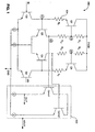
- FIG. 1 is a schematic diagram of a bipolar amplifier.
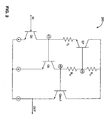
- FIG. 2 is a schematic diagram of a bipolar "hay circuit,” taken from the bipolar amplifier illustrated in FIG. 1.
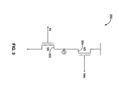
- FIG. 3 is a schematic diagram of a CMOS gain stage leg 300, in accordance with the invention.
- FIG. 4 is a schematic diagram of a CMOS gain stage 400, in accordance with the invention.
- FIG. 5 is another schematic diagram of the CMOS gain stage 400, including gain resistors R L1 and R L2 .
- FIG. 6 is another schematic diagram of the CMOS gain stage 400, including optional PVT variation protection circuitry in place of the resistors R L1 and R L2 .
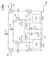
- FIG. 7 is another schematic diagram of the CMOS gain stage 400, wherein a source follower circuit is omitted and a bias network is configured with resistive divider circuits to insure proper saturation of an input device of a subsequent gain stage.
- FIG. 8 is another schematic diagram of the CMOS gain stage 400, including optional drain-to-bulk junction punch-through protection circuitry that protects output transistors from drain-to-bulk junction punch-through.
- FIG. 9 is another schematic diagram of the CMOS gain stage 400, including additional optional drain-to-bulk junction punch-through protection circuitry that protects input transistors from drain-to-bulk junction punch-through.
- FIG. 10 is another schematic diagram of the CMOS gain stage 400, including optional bandwidth enhancement circuitry.
- FIG. 1 is a schematic diagram of a bipolar amplifier 100.
- FIG. 2 is a schematic diagram of a bipolar "hay circuit" 200, which is taken from the bipolar amplifier 100 in FIG. 1.
- a gain of the bipolar amplifier 100 can be determined by analyzing the hay circuit 200.
- the hay circuit 200 includes bipolar transistors Q3, Q5, and Q7, and resistors R L1 and R L2 .
- Transconductances of the transistors Q3, Q5, Q7 are denoted as gm 3 , gm 5 , and gm 7 , respectively.
- the gain " G " of the hay circuit 200 is given by equation 2:
- the bipolar amplifier 100 (FIG. 1) has a relatively high bandwidth because each of nodes n1-n4 has a low impedance. As a result, the poles contributed at each node by the presence of transistor junction capacitances and parasitic capacitances occur at relatively high frequencies, which leads to less bandwidth loss.
- node n2 for example.
- the real impedance at node n2 is give by equation 6: R L 1 + R L 2 gm 5 ( R L 1 + R L 2 )
- Equation 6 can be approximated as 1/ gm 5, which tends to be a relatively low value compared to (R L1 + R L2 ), because gm 5 tends to be relatively large.
- the denominator in equation 7 is not [1+ gm 5 (R L1 + R L2 )], because the feedback is closed at the output of R L1 only. At node n1, therefore, the impedance value is also relatively low, being divided by approximately the internal amplifier gain.
- a resistor 104 also denoted as resistor R F , is placed in series with load transistor Q7. This provides a gain >1 in that branch.
- RF 0
- the gain of the leg then drops to gm3/gm7. Since the same current flows through both Q3 and Q7, their transconductances (gm) are equal, resulting in a gain of 1.
- FIG. 3 is a schematic diagram of a CMOS gain stage leg 300, in accordance with the invention.
- the gain of the CMOS gain stage leg 300 is gm 1 /gm 3 , where gm 1 is a transconductance of a first CMOS device 302, also denoted as M1, and gm 3 is a transconductance of a second CMOS device 304, also denoted as M3.
- transconductances (gm) of MOSFET devices can be different from one another, even when the MOSFET devices carry the same current. This is accomplished by appropriately sizing the width/length (w/l) ratios of the devices.
- the relatively sizable gain in the CMOS gain stage leg 300 can be obtained without a series resistor. In CMOS implementations, therefore, the resistor RF (FIG. 1) is not needed.
- CMOS gain stage leg 300 Another advantage of the CMOS gain stage leg 300 is that transconductances of MOSFET devices can be made to track one another over process, voltage, and temperature variations.
- the CMOS gain stage leg 300 is thus less process-dependent than bipolar devices, where the gain was proportional to gm 3 R F .
- Non-linearities of gm 1 and gm 3 in the CMOS gain stage leg 300 tend to cancel one another out to some extent.
- FIG. 4 is a schematic diagram of a CMOS gain stage 400 in accordance with the invention.
- the CMOS gain stage 400 incorporates the CMOS gain stage leg 300 of FIG. 3.
- the CMOS gain stage 400 includes first and second input nodes 402 and 404, respectively, which receive a differential signal Vip and Vin.
- the first and second input nodes 402 and 404 receive a single-ended signal, wherein a signal is provided to one of the input nodes 402, 404, and the other input node is coupled to a fixed supply, such as a voltage supply or a ground.
- connection When used herein, the terms “connected” and/or “coupled” are generally used to refer to electrical connections. Such electrical connections can be direct electrical connections with no intervening components, and/or indirect electrical connections through one or more components.
- the CMOS gain stage 400 also includes first and second input CMOS transistors 406 and 408, respectively, also denoted as M1 and M4, respectively.
- the first and second input CMOS transistors 406 and 408 include gate terminals coupled to the first and second input nodes 402, 404, respectively.
- Source terminals of the input transistors M1 and M4 are coupled to an input stage current source 410.
- the CMOS gain stage 400 further includes first and second feedback-controlled CMOS transistors 412 and 414, respectively, also denoted as M3 and M6, respectively.
- the first and second feedback-controlled CMOS transistors 412 and 414 include source terminals coupled to respective drain terminals of the input transistors M1 and M4.
- Gate terminals of the first and second feedback-controlled transistors M3 and M6 are coupled to a bias network 418, which is described below.
- Drain terminals of the feedback-controlled transistors M3 and M6 are coupled to a supply node 416, directly or through optional drain-to-bulk junction punch-through protection circuitry 428, which is described below.
- the CMOS gain stage 400 further includes first and second output transistors 420 and 422, respectively, also denoted as M2 and M5, respectively.
- Source terminals of the first and second output transistors M2 and M5 are coupled to an output stage current source 425.
- Gate terminals of the first and second output transistors M2 and M5 are coupled to the drain terminals of the first and second input transistors M1 and M4, respectively.
- Drain terminals of the first and second output transistors M2 and M5 are coupled to the supply node 416, directly or through a load, which can include optional drain-to-bulk junction punch-through protection circuitry 430, optional process, voltage, and/or temperature (“PVT") variation protection circuitry 432, and/or optional bandwidth enhancement circuitry 434, all of which are described below.
- Drain terminals of the first and second output transistors M2 and M5 are coupled to first and second output nodes 424 and 426, respectively, are also denoted as "OP 1" "ON1.”
- Bias network 418 is coupled between the gate terminals of the feedback-controlled transistors M3 and M6, and the output nodes 424 and 426.
- the bias network 418 biases the transistors M3 and M6 to insure proper saturation of an output source-follower 436, discussed below, and/or of an input device of a subsequent gain stage, also discussed below.
- An input device (e.g., transistor) of a subsequent gain stage should be maintained in saturation because transistors have higher transconductances (i.e., gm) and thus larger gains, in saturation.
- the output source-follower 436 helps to insure proper saturation of an input device of a subsequent stage.
- the output source-follower 436 includes first and second source-follower input nodes 438 and 440, also denoted “ON1” and “OP1,” respectively.
- the output source-follower input nodes 438 and 440 are coupled to the output nodes 424 and 426, respectively.
- the output source-follower 436 includes first and second source-follower output nodes 442 and 444, respectively, also denoted "ON” and "OP,” respectively.
- the source-follower output nodes 442 and 444 serve as the output nodes of the CMOS gain stage 400.
- the first and second output nodes 424 and 426 serve as the output nodes of the CMOS gain stage 400.
- the output nodes of the CMOS gain stage 400 can be coupled to input devices of a subsequent gain stage.
- Output source followers are difficult to implement in CMOS circuits due to limitations described herein. Output source followers also consume power and tend to degrade performance.
- the source follower 436 is optionally omitted by configuring the biasing circuitry 418 to insure proper saturation of an input device of a subsequent stage, without use of the source follower 436. This is described below with reference to FIG. 7.
- the input transistors M1 and M4, and the feedback-controlled transistors M3 and M6 form an input stage of the CMOS gain stage 400.
- the first input transistor M1 and the first feedback-controlled transistors M3 form a first leg of the input stage.
- the first leg of the input stage includes a node 446, also denoted n1.
- the node n1 serves as an output of the input stage.
- the first leg of the input stage has a gain that can be defined as a ratio between an input signal level at the first input node 402 and a signal level at the node n1.
- the gain of the first leg of the input stage is a function of transistors M1 and M3, and of the optional drain-bulk junction punch-through protection circuitry 428, as described below.
- An output stage of the CMOS gain stage 400 is formed by the output transistors M2 and M5, the output source follower 436 (when implemented), the bias network 418, the optional drain-to-bulk junction punch-through protection circuitry 430, the optional PVT variation protection circuitry 432, and the optional band-width enhancement circuitry 434.
- a first leg of the output stage is formed by the transistor M2, and relevant portions of the bias network 418, the optional drain-to-bulk junction punch-through protection circuitry 430, the optional PVT variation protection circuitry 432, and the optional band-width enhancement circuitry 434.
- the first leg of the output stage has a gain that can be defined as a ratio between a signal level at the node n1, and a signal level at the output node 424.
- the gain of the first leg of the output stage is a function of the transistor M2, the bias network 418, the optional drain-to-bulk junction punch-through protection circuitry 430, the optional PVT variation protection circuitry 432, and the optional band-width enhancement circuitry 434, as described below.
- the CMOS gain stage 400 receives a differential signal, single-ended or double-ended, at the input nodes 402 and 404.
- the CMOS gain stage 400 outputs a differential signal, single-ended or double-ended, at the output nodes 424 and 426.
- a potential difference between the output nodes 424 and 426 is "gained-up" from a potential difference between the input nodes 402 and 404.
- the CMOS gain stage 400 can be configured with one or more of a variety optional features.
- the CMSO gain stage 400 is powered by a relatively high supply voltage, as described above.
- the CMOS gain stage 400 can include the optional drain-to-bulk junction punch-through protection circuitry 430 to avoid potential drain-to-bulk punch-through that could otherwise occur for devices M2 and M5.
- the optional drain-to-bulk junction punch-through protection circuitry 430 can also be implemented to substantially prevent a gate-to-source capacitance, Cgs, of transistors within the PVT variation protection circuitry 432 from appearing at the output. This is described below with reference to FIG. 8.
- the CMOS gain stage 400 can include the optional drain-to-bulk junction punch-through protection circuitry 428 to avoid potential drain-to-bulk punch-through that could otherwise occur for devices M3 and M6. This is described below with reference to FIG. 9.
- the CMOS gain stage 400 can include the optional PVT variation protection circuitry 432, which renders a gain of the CMOS gain stage 400 relatively independent of process, voltage, and/or temperature variations. This is described below with reference to FIG. 6.
- the CMOS gain stage 400 can include the optional bandwidth enhancement circuitry 434 is described below with reference to FIG. 10.
- the optional features described herein can be implemented alone and/or in various combinations with one another.
- FIG. 5 is a schematic diagram of the CMOS gain stage 400 wherein the bias network 418 is configured to operate with the output source-follower 436.
- the output source-follower 436 helps to insure proper saturation of an input device of a subsequent stage, as described below.
- the bias network 418 includes a plurality of series-connected resistances 502, 504, and 505, also denoted here as x • R L2 , 2 • R L2 , and x • R L2 , respectively.
- the plurality of series-connected resistances 506, 508, and 510 in conjunction with the resistances 502 and 504, contribute to the gain of the CMOS gain stage 400.
- the CMOS gain stage 400 also includes resistances 502 and 504, which are also denoted as R L1 and R L2 .
- the resistances R L1 and R L2 provide gain advantages as described above.
- the resistances R L1 and R L2 can be omitted when the optional PVT variation protection circuitry 432 is utilized, as described below.
- the gain of the first leg of the input stage is equal to gm 1 /gm 3 . Since M3 and M1 are typically on the same integrated circuit chip, PVT variations tend to affect M1 and M3 to the same degree. These affects tend to cancel one another out. The gain gm 1 /gm 3 is thus relatively independent of PVT variations. Additionally, non-linearities tend to cancel out.
- the output source follower 436 can be used to drive another similar gain stage. To ensure that input devices of the next stage are held in saturation, the voltage at the outputs OP and ON should not be too high. Using approximate replica biasing, which is described below, the source-follower 436 substantially ensures that the nodes n1 and n2 of a subsequent gain stage are close to a common mode of the output nodes OP and ON, thus insuring the correct output level (i.e., the input to the subsequent stage), to maintain input devices of the subsequent stage in saturation.
- the OP and ON voltage should be roughly equal to the voltage at nodes n1 and n2, respectively.
- the gate common mode voltage is essentially the same as the common mode at OP1 and ON1. This is because of the connections between the resistors in the bias network 418, so there is no drop across the resistors, common mode wise.
- the gate voltage of M3 is essentially the same as the voltage at OP1, common mode wise, but not necessarily differentially. Therefore, the node n1 is 1 vgs drop below the common mode of OP1 and ON1.
- M7 and M8 produce the output voltage Op and On, which is 1 vgs below OP1 and ON1. This is what is meant by replica biasing.
- the voltages OP and ON are essentially the same common mode voltage as node n1 and n2. That is the purpose of the source follower 436.
- the source follower 436 maintains essentially the same common mode at the output as node n1.
- Inputs OP and ON of the subsequent stage will have their own associated nodes n1 and n2, but the OP and ON are such that they are about equal to the n1 and n2 of the next stage. This insures that the input device of the next stage will be held in saturation. This is a reason for using the source follower.
- Other potential purposes of the source follower 436 include low impedance output to the subsequent stage so it can drive the next stage easily.
- Source follower 436 can be compared to a leg formed by transistor M3.
- M3 and M7 are sized proportional to their respective DC currents to insure similar vgs drops. This assures that the OP and ON common mode voltages are substantially equal to n1 and n2 common mode voltages. Nodes n1 and n2 of a subsequent stage are close to a common mode of the output OP and ON.
- gmb 7 is a transconductance parameter modeled to incorporate the body effect of M7
- gds 9 is a drain-to-source conductance of M9.
- the output source-follower 436 is suitable for many applications. In CMOS implementations, however, design considerations favor omission of the optional source-follower 436. For example, in MOS implementations, source-followers tend to be difficult to design for high speed operation. This is due to a relatively strong body effect of the transistor M7 and to the finite output resistance of device M9 in deep sub-micron technology. This tends to result in gain reduction. Moreover, transconductances in MOS technology tend to be much smaller than in bipolar technology. As a result, driving the transistor junction, the gate capacitance, and the parasitic capacitance is difficult, causing the CMOS gain stage 400 to lose speed. The gain and speed issues can be overcome, at least to some extent, with various circuit techniques. Nevertheless, real estate requirements and power consumption can be reduced by performing the functions of the source-follower 436 with other techniques. Other considerations may also lead a designer to want to use other techniques to perform the functions of the source-follower 436, as described below.
- equation 11 simplifies to equation 12.
- the gain depends on ratios rather than absolute parameters, and is thus relatively PVT independent.
- R L1 is typically kept relatively low.
- the transconductance gm 2 is generally lower than in bipolar transistors. In such situations, 1/gm 2 R L1 becomes almost comparable to "X,” and hence cannot be ignored. In at least these situations, the optional source-follower 436 can be advantageously omitted as described below with respect to FIG. 7.
- FIG. 7 is a schematic diagram of the CMOS gain stage 400, wherein the source follower is omitted and the bias network 418 is configured with resistive divider circuits coupled between the supply node 416 and the output nodes 420 and 422.
- the resistive divider circuits bias M3 and M6.
- a first resistive divider circuit includes resistances 702 and 704, and a node n5 there between.
- a second resistive divider circuit includes resistances 706 and 708, and a node n6 there between.
- the first resistive divider circuit is coupled between the supply node 416 and the drain terminal of M2.
- the second resistive divider is coupled between the supply node 416 and the drain terminal of M5.
- Nodes n5 and n6 are coupled to respective gate terminals of M3 and M6. This configuration of bias network 418 raises the common mode at the nodes n5 and n6, which is supplied to the gates of M3 and M6.
- trickle biasing This is referred to herein as trickle biasing.
- OP1 and ON1 thus come close to the common mode of n1 and n2, which insures saturation of the input devices to the next stage.
- the resistive divider circuits perform an approximate function of providing a common mode voltage raise approximately equal to the vgs drops of M3 and M5.
- an input device e.g., transistor
- gm transconductances
- replica biasing provided by the output source follower 436 insures saturation of an input device of a subsequent stage.
- the source follower has been omitted. Instead, the bias network 418 provides feedback control so that OP1 and ON1 are at a common mode voltage, which insures that an input device of a subsequent stage is held in saturation.
- a transistor is in a saturation condition when the drain voltage (Vd) of the transistor is greater than the gate voltage (Vg) minus the threshold of the transistor (Vt), as illustrated by equation (13): Vd > Vg-Vt
- the inequality of equation (13) is satisfied for any positive threshold voltage Vt.
- Vg-Vt 300 mv.
- Vd 500mv
- Vg-Vt 300 mv
- Vd 500mv
- Vg-Vt 300 mv
- Vd 500mv
- Vg-Vt 300 mv
- threshold voltages are typically in the range of about 300mv to 400mv, although threshold voltages tend to be foundry-process-dependent. So for 0.13 ⁇ m technology, the inequality of equation (13) will be satisfied for any Vd that is greater than Vg minus 300mv to 400mv.
- the invention is not, however, limited to 0.13 ⁇ m technology.
- Th voltage at n1 is approximately equal to the voltage at OP1, plus the resistive divider voltage at node 5, minus the voltage (Vgs) across M3.
- the resistive divider is designed so that the voltage at node 5 is maintained relatively close to the voltage (Vgs) across M3.
- the voltage at n1 is thus maintained approximately equal to the voltage at OP1.
- the voltage at node n1 is typically less than or equal to the voltage at OP1. Since, OP1 is maintained close to the bias of node n1, the inequality of equation (13) is satisfied. Since OP1 is providing the input Vip to a subsequent stage, an input device of the subsequent stage will be maintained in saturation.
- transistors are illustrated with their bodies tied to their respective source terminals. This helps to avoid body effects of the transistors.
- the body-to-source ties are not essential, but can be useful in many applications.
- the supply node 416 should be coupled to a supply that is equal to or greater than: 2Vgs + 1 Vds + 2IR drop
- Vgs is the gate-to-source voltage for M2 and M3
- Vds is the drain to source voltage for M2
- IR drop is a voltage drop across the resistors X•R L2 , and R L1 .
- the supply node 416 should be greater than 2 volts to support these drops.
- Deep sub-micron process technologies generally do not normally support higher supply voltages. Thus, it is unconventional to use such a large voltage for deep sub-micron process technologies, such as 0.13 ⁇ m process technologies, for example.
- Reasons for this include potential gate oxide breakdown, drain-to-bulk junction punch-through, and source-to-bulk junction punch-through, all which can happen at relatively low voltages.
- Gate oxide breakdown depends on the gate to source voltage of the transistor, which should not exceed a certain amount (e.g., less than 2 volts for 0.13 ⁇ m process technologies).
- Drain-to-bulk junction punch-through depends on the drain to bulk voltage.
- Source-to-bulk junction punch-through depends on the source to bulk voltage.
- the latter is not typically an issue, however, because the source voltage is typically below the drain voltage and is not generally coupled directly to the power supply.
- the drain and gate voltages can be at higher voltages, possibly even coupled directly to the power supply. Where the power supply is a relatively high supply voltage, breakdown could occur absent protection.
- CMOS gain stage which is coupled to a supply voltage that exceeds the foundry-permitted supply voltage for a give processes technology, includes protection circuitry.
- Gate oxide breakdown is prevented with protection circuitry that prevents Vgs from exceeding the threshold.
- Drain-to-bulk junction punch through is prevented by insuring that drain-to-bulk voltage never exceeds the threshold. Drain-to-source bulk junction punch-through can be avoided with the optional drain-to-bulk junction punch-through protection circuitry 430, as described below with respect to FIG. 8, and/or with the optional drain-to-bulk junction punch-through protection circuitry 428, described below with respect to FIG. 9.
- the drain-to-bulk junction protection circuitry illustrated in FIGS. 8 and 9 have the added advantage of providing gate oxide breakdown protection as well.
- gate oxide breakdown protection circuitry and/or drain-to-bulk junction punch-through protection circuitry is designed to protect one or more of M1 through M6.
- M3 and M6 are protected by drain-to-bulk junction punch-through protection circuitry 428, which also protects M1 and M4.
- M2 and M5 are protected by drain-to-bulk junction punch-through protection circuitry 430.
- drain-to-bulk junction punch-through protection of M2 and M5 is provided by PVT variation protection circuitry 432, as described below.
- PVT variation protection circuitry 432 as described below.
- the invention is not, however, limited to the examples provided herein. Based on the description herein, one skilled in the relevant arts) will understand that other circuitry can be utilized to provide gate oxide breakdown protection, including drain-to-bulk junction punch-through protection and/or source-to-bulk junction punch-through protection.
- the CMOS gain stage 400 includes the optional drain-to-bulk junction punch-through protection circuitry 430, which protects M2 and M5 from drain-to-bulk junction punch-through.
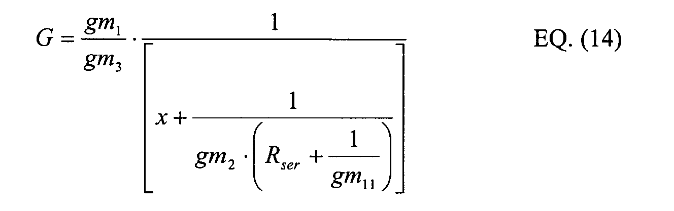
- the optional drain-to-bulk junction punch-through protection circuitry 430 includes first and second series resistances 802 and 803, also denoted as R Ser1 , between the drain terminals of M2 and M5 and the supply node 416.
- the resistances R Ser1 reduce the voltage at the drain terminals of M2 and M5. The reduced voltage reduces the potential drain-to-bulk punch-through that could otherwise occur for devices M2 and M5.
- the optional PVT variation protection circuitry 432 is implemented as in FIG. 6, the series resistances R Ser1 also substantially prevent the gate-to-source capacitance of M11 and M12 from appearing directly at the output nodes 424 and 426.
- the gain of the CMOS gain stage 400 is given by equation 14.
- the resistances R ser should be relatively small, for example, less than 1/gm 11 or 1/gm 12 , so that it limits gain sensitivity to PVT variations.
- the CMOS gain stage 400 further includes the optional drain-to-bulk junction punch-through protection circuitry 428, which protects M3 and M6 from drain-to-bulk junction punch-through.
- the optional drain-to-bulk junction punch-through protection circuitry 428 includes a common mode resistance 902, also denoted as R CM , coupled between the supply node 416 and the drain terminals of M3 and M6.
- R CM common mode resistance
- the common mode resistance R CM reduces the voltage at the drain terminals of M3 and M6, and thus helps to prevent drain-to-bulk punch-through of M3 and M6.
- Drain-to-bulk junction punch-through protection and gate oxide breakdown protection is typically implemented on a transistor by transistor basis.
- each transistor in the circuit is provided with protection circuitry, as needed.
- an integrated circuit (“IC") chip includes additional transistors besides those in the CMOS gain stage 400, the additional transistors can be provided with protection as well.
- the drain-to-bulk junction circuitry also provides gate oxide breakdown protection.
- the gate and drain of M11 are coupled together, and the bulk and source of M11 are tied together.
- the drain-to-bulk junction voltage of M11 is the same as the gate to source voltage of M11.
- the drain-to-bulk junction circuitry prevents the drain-to-bulk junction voltage from exceeding the threshold, it also necessarily prevents the gate to source voltage from exceeding the threshold.
- FIG. 6 illustrates the CMOS gain stage 400, including the optional PVT variation protection circuitry 432.
- the optional PVT variation circuitry 430 renders the gain of the CMOS gain stage 400 relatively independent of PVT variations.
- the optional PVT variation protection circuitry 432 includes first and second diode-connected transistors 602 and 604, respectively, also denoted as M11 and M12, coupled between the supply node 416 and respective drain terminals of the transistors output M2 and M5.
- the diode-connected transistors M11 and M12 provide similar gain characteristics as the resistors 502 and 504 in FIG. 5.
- CMOS gain stage 400 relatively independent of PVT variations.
- the PVT variation protection circuitry 432 also provides a measure of drain-to-bulk junction punch-through protection for M2 and M5.
- FIG. 10 illustrates the CMOS gain stage 400, including the optional bandwidth enhancement circuitry 434.
- the optional bandwidth enhancement circuitry 434 includes gate resistances 1002 and 1004, also denoted as R GATE , coupled between the supply node 416 and respective gates of the diode-connected transistors M11 and M12.
- the gate resistances R gate in combination with the diode-connected transistors M11 and M12, behave similar to an active inductor. See S. Hara, IEEE Transactions on Microwave Theory and Techniques, Vol. 36, No. 12, Dec. 1988, incorporated herein by reference in its entirety.
Landscapes
- Engineering & Computer Science (AREA)
- Power Engineering (AREA)
- Amplifiers (AREA)
- Metal-Oxide And Bipolar Metal-Oxide Semiconductor Integrated Circuits (AREA)
Abstract
Description




Claims (20)
- A CMOS gain stage, comprising:first and second input nodes;first and second input CMOS transistors having gate terminals coupled to said first and second input nodes, respectively;first and second feedback-controlled CMOS transistors having drain terminals coupled to a supply node and source terminals coupled to drain terminals of said first and second input CMOS transistors, respectively;first and second output CMOS transistors having gate terminals coupled to said drain terminals of said first and second input CMOS transistors, respectively, and drain terminals coupled to said supply node, wherein said first and second output CMOS transistor drain terminals form first and second output nodes, respectively; anda bias network coupled between gate terminals of said first and second feedback-controlled CMOS transistors, wherein said bias network is configured to bias said first and second feedback-controlled CMOS transistors to insure saturation of an input device in a subsequent stage without use of a source-follower circuit.
- The apparatus according to claim 1, wherein said bias network comprises first and second resistive divider circuits, each including first and second series-connected resistances coupled between said supply node and respective said drain terminals of said first and second output CMOS transistors, said first and second resistive divider circuits including first and second divider nodes, respectively, coupled to respective gate terminals of said first and second feedback-controlled CMOS transistors.
- The apparatus according to claim 2, wherein said supply node is coupled to a voltage source that is greater than a permitted supply voltage for a processes technology that is used to fabricate said apparatus, said apparatus further comprising drain-to-bulk junction punch-through protection circuitry coupled between said supply node and respective said first and second output CMOS transistor drain terminals.
- The apparatus according to claim 3, wherein the drain-to-bulk junction punch-through protection circuitry provides gate-oxide breakdown protection.
- The apparatus according to claim 3, wherein said drain-to-bulk junction punch-through protection circuitry comprises:a third resistance coupled between said supply node and said first output CMOS transistor drain terminal; anda fourth resistance coupled between said supply node and said second output CMOS transistor drain terminal.
- The apparatus according to claim 5, wherein said drain-to-bulk junction punch-through protection circuitry further comprises a first diode connected transistor coupled between said supply node and said third resistance and a second diode connected transistor coupled between said supply node and said fourth resistance.
- The apparatus according to claim 6, further comprising first and second gate resistances coupled between said supply node and respective gate terminals of said first and second diode connected transistors.
- The apparatus according to claim 3, wherein said drain-to-bulk junction punch-through protection circuitry comprises first and second diode connected transistors coupled between said supply node and respective said first and second output CMOS transistor drain terminals.
- The apparatus according to claim 8, further comprising first and second gate resistances coupled between said supply node and respective gate terminals of said first and second diode connected transistors.
- The apparatus according to claim 2, wherein said supply node is coupled to a voltage source that is greater than a permitted supply voltage for a processes technology that is used to fabricate said apparatus, said apparatus further comprising drain-to-bulk junction punch-through protection circuitry coupled between said supply node and said first and second feedback-voltage-controlled CMOS transistor drain terminals.
- The apparatus according to claim 10, wherein said drain-to-bulk junction punch-through protection circuitry provides gate-oxide breakdown protection.
- The apparatus according to claim 10, wherein said drain-to-bulk junction punch-through protection circuitry comprises a third resistance coupled between said supply node and said first and second feedback-voltage-controlled CMOS transistor drain terminals.
- The apparatus according to claim 3, further comprising second drain-to-bulk junction punch-through protection circuitry coupled between said supply node and said first and second feedback-voltage-controlled CMOS transistor drain terminals.
- The apparatus according to claim 13, wherein said first drain-to-bulk junction punch-through protection circuitry includes a third resistance coupled between said supply node and said first output CMOS transistor drain terminal, and a fourth resistance coupled between said supply node and said second output CMOS transistor drain terminal, and wherein said second drain-to-bulk junction punch-through protection circuitry comprises a fifth resistance coupled between said supply node and said first and second feedback-voltage-controlled CMOS transistor drain terminals.
- A CMOS gain stage, comprising:first and second input nodes;first and second input CMOS transistors having gate terminals coupled to said first and second input nodes, respectively;first and second feedback-controlled CMOS transistors having drain terminals coupled to a supply node and source terminals coupled to drain terminals of said first and second input CMOS transistors, respectively, wherein said supply node is coupled to a voltage supply that is greater than a permitted supply voltage for a processes technology that is used to fabricate said apparatus;first and second output CMOS transistors having gate terminals coupled to said drain terminals of said first and second input CMOS transistors, respectively, and drain terminals that form first and second output nodes, respectively;a bias network including first and second resistive divider circuits, each including first and second series-connected resistances coupled between said supply node and respective drain terminals of said first and second output CMOS transistors, said first and second resistive divider circuits including first and second divider nodes, respectively, coupled to respective gate terminals of said first and second feedback-controlled CMOS transistors, wherein said bias network biases said first and second feedback-controlled CMOS transistors to insure saturation of an input device in a subsequent stage without use of a source-follower circuit;first drain-to-bulk junction punch-through protection circuitry including third and fourth resistances coupled between said supply node and said first and second output CMOS transistor drain terminals, respectively, in parallel with said bias network;second drain-to-bulk junction punch-through protection circuitry including a fifth resistance coupled between said supply node and said first and second feedback-voltage-controlled CMOS transistor drain terminals;process-voltage-temperature ("PVT") variation protection circuitry coupled between said supply node and said first drain-to-bulk junction punch-through protection circuitry, said PVT variation protection circuitry including first and second diode-connected CMOS transistors having drain and gate terminals coupled to said supply node, and source terminals coupled to said first drain-to-bulk junction punch-through protection circuitry; andbandwidth enhancement circuitry, including sixth and seventh resistors coupled between said supply node and respective gate terminals of said first and second diode connected CMOS transistors.
- A common mode CMOS gain stage, comprising:a CMOS input stage;a CMOS output stage coupled to said CMOS input stage; anda bias network coupled between said CMOS input stage and said CMOS output stage, said bias network configured to insure saturation of an input stage of a subsequent gain stage without use of a source-follower circuit, wherein the input stage of the subsequent stage is configured similarly to said CMOS input stage.
- The apparatus according to claim 16, wherein said common mode CMOS gain stage is powered by a supply voltage that is greater than a permitted supply voltage for a processes technology that is used to fabricate said apparatus , said apparatus further comprising:first drain-to-bulk junction punch-through protection circuitry coupled to said CMOS input stage; andsecond drain-to-bulk junction punch-through protection circuitry coupled to said CMOS output stage.
- The apparatus according to claim 17, further comprising;process-voltage-temperature ("PVT") variation protection circuitry coupled to said CMOS output stage.
- A method for operating a CMOS implemented gain stage implemented substantially as recited in claim 1, comprising:(1) providing a supply voltage to said CMOS implemented gain stage that is greater than a permitted supply voltage for a processes technology that is used to fabricate said CMOS implemented gain stage, wherein said supply voltage accomodates Vgs, Vds and IR voltage drops in said CMOS implemented gain stage;(2) receiving a differential signal at said first and second input nodes;(3) protecting transistors in said CMOS implemented gain stage from drain-to-bulk junction punch through and gate oxide breakdown;(4) outputting a gained-up differential signal from said first and second output nodes;(5) providing said gained-up differential signal to an input device in a subsequent stage; and(6) biasing said first and second feedback-controlled CMOS transistors using said bias network to insure saturation of said input device in said subsequent stage without use of a source-follower circuit.
- A method for operating a CMOS implemented gain stage implemented substantially as recited in claim 1, comprising:means for providing a supply voltage to said CMOS implemented gain stage that is greater than a permitted supply voltage for a processes technology that is used to fabricate said CMOS implemented gain stage, wherein said supply voltage accomodates Vgs, Vds and IR voltage drops in said CMOS implemented gain stage;means for receiving a differential signal at said first and second input nodes;means for protecting transistors in said CMOS implemented gain stage from drain-to-bulk junction punch through and gate oxide breakdown;means for outputting a gained-up differential signal from said first and second output nodes;means for providing said gained-up differential signal to an input device in a subsequent stage; andmeans for biasing said first and second feedback-controlled CMOS transistors using said bias network to insure saturation of said input device in said subsequent stage without use of a source-follower circuit.
Applications Claiming Priority (2)
| Application Number | Priority Date | Filing Date | Title |
|---|---|---|---|
| US10/226,228 US6927631B2 (en) | 2002-08-23 | 2002-08-23 | Wideband CMOS gain stage |
| US226228 | 2002-08-23 |
Publications (3)
| Publication Number | Publication Date |
|---|---|
| EP1391985A2 true EP1391985A2 (en) | 2004-02-25 |
| EP1391985A3 EP1391985A3 (en) | 2004-07-21 |
| EP1391985B1 EP1391985B1 (en) | 2009-07-22 |
Family
ID=31188015
Family Applications (1)
| Application Number | Title | Priority Date | Filing Date |
|---|---|---|---|
| EP03019211A Expired - Lifetime EP1391985B1 (en) | 2002-08-23 | 2003-08-25 | Wideband cmos gain stage |
Country Status (3)
| Country | Link |
|---|---|
| US (3) | US6927631B2 (en) |
| EP (1) | EP1391985B1 (en) |
| DE (1) | DE60328441D1 (en) |
Families Citing this family (11)
| Publication number | Priority date | Publication date | Assignee | Title |
|---|---|---|---|---|
| US6784749B1 (en) * | 2003-02-24 | 2004-08-31 | Intel Corporation | Limiting amplifier with active inductor |
| US7091773B1 (en) * | 2004-07-28 | 2006-08-15 | Xilinx, Inc. | Limiting circuit with level limited feedback |
| US7388387B2 (en) * | 2006-01-11 | 2008-06-17 | Stratosphere Solutions, Inc. | Method and apparatus for measurement of electrical resistance |
| US7453315B2 (en) * | 2006-04-26 | 2008-11-18 | Infineon Technologies Ag | Active inductive load that enhances circuit bandwidth |
| US7522003B2 (en) * | 2006-12-26 | 2009-04-21 | Texas Instruments Incorporated | Constant margin CMOS biasing circuit |
| TWI334692B (en) * | 2007-02-06 | 2010-12-11 | Realtek Semiconductor Corp | Dynamic voltage-generating apparatus and method thereof |
| JP5743850B2 (en) * | 2011-10-28 | 2015-07-01 | 株式会社東芝 | Integrated circuit |
| US8975952B2 (en) | 2012-11-13 | 2015-03-10 | Honeywell International Inc. | CMOS logic circuit using passive internal body tie bias |
| US8742848B1 (en) * | 2013-03-14 | 2014-06-03 | Linear Technology Corporation | Common mode rejection ratio versus frequency in instrumentation amplifier |
| KR102340344B1 (en) * | 2015-02-05 | 2021-12-21 | 한국전자통신연구원 | Reconfigurable power amplifier apparatus and a method for wide band frequency selection |
| KR102678310B1 (en) * | 2019-06-11 | 2024-06-25 | 삼성전자주식회사 | Switching transformer and electronic device including thereof |
Family Cites Families (7)
| Publication number | Priority date | Publication date | Assignee | Title |
|---|---|---|---|---|
| US4427903A (en) | 1980-06-24 | 1984-01-24 | Nippon Electric Co., Ltd. | Voltage current converter circuit |
| IT1201839B (en) * | 1986-08-08 | 1989-02-02 | Sgs Microelettronica Spa | OPERATIONAL AMPLIFIER OF CMOS POWER WITH FULLY DIFFERENTIAL OUTPUT |
| EP0598445B1 (en) | 1992-11-17 | 1998-02-11 | Koninklijke Philips Electronics N.V. | MOS technology amplifier circuit |
| US5917376A (en) * | 1997-08-22 | 1999-06-29 | Burr-Brown Corporation | Circuit and technique for compensating high gain amplifier without compensation capacitors |
| US6509796B2 (en) * | 2000-02-15 | 2003-01-21 | Broadcom Corporation | Variable transconductance variable gain amplifier utilizing a degenerated differential pair |
| US6292033B1 (en) | 2000-10-11 | 2001-09-18 | Intersil Corporation | Precision, low-power transimpedance circuit with differential current sense inputs and single ended voltage output |
| US6509795B1 (en) * | 2001-09-26 | 2003-01-21 | Texas Instruments Incorporated | CMOS input stage with wide common-mode range |
-
2002
- 2002-08-23 US US10/226,228 patent/US6927631B2/en not_active Expired - Fee Related
-
2003
- 2003-08-25 EP EP03019211A patent/EP1391985B1/en not_active Expired - Lifetime
- 2003-08-25 DE DE60328441T patent/DE60328441D1/en not_active Expired - Lifetime
-
2005
- 2005-06-24 US US11/165,493 patent/US7205840B2/en not_active Expired - Fee Related
-
2007
- 2007-04-10 US US11/783,601 patent/US8138839B2/en not_active Expired - Fee Related
Also Published As
| Publication number | Publication date |
|---|---|
| EP1391985B1 (en) | 2009-07-22 |
| US8138839B2 (en) | 2012-03-20 |
| DE60328441D1 (en) | 2009-09-03 |
| US6927631B2 (en) | 2005-08-09 |
| EP1391985A3 (en) | 2004-07-21 |
| US20040036534A1 (en) | 2004-02-26 |
| US20050258902A1 (en) | 2005-11-24 |
| US20070188232A1 (en) | 2007-08-16 |
| US7205840B2 (en) | 2007-04-17 |
Similar Documents
| Publication | Publication Date | Title |
|---|---|---|
| US8138839B2 (en) | Wideband CMOS gain stage | |
| Raikos et al. | 0.5 V bulk-driven analog building blocks | |
| US5734296A (en) | Low voltage operational amplifier input stage and method | |
| US4048575A (en) | Operational amplifier | |
| JP5798635B2 (en) | Current mirror and high compliance single stage amplifier | |
| US6433637B1 (en) | Single cell rail-to-rail input/output operational amplifier | |
| JP4578703B2 (en) | Operational amplifier | |
| EP0045841A1 (en) | Linear voltage-current converter | |
| JP3214474B2 (en) | Operational amplifier circuit | |
| US6005439A (en) | Unity gain signal amplifier | |
| US9401679B1 (en) | Apparatus and method for improving power supply rejection ratio | |
| US8022764B2 (en) | Differential amplifier | |
| KR20070057022A (en) | Low Voltage Low Power A / V Output | |
| US6583669B1 (en) | Apparatus and method for a compact class AB turn-around stage with low noise, low offset, and low power consumption | |
| US6545502B1 (en) | High frequency MOS fixed and variable gain amplifiers | |
| Likittanapong et al. | Linear CMOS triode transconductor for low-voltage applications | |
| US6696895B2 (en) | Push-pull amplifier | |
| US7259626B2 (en) | Apparatus and method for biasing cascode devices in a differential pair using the input, output, or other nodes in the circuit | |
| US6876182B1 (en) | MOSFET current mirror circuit with cascode output | |
| US11228283B2 (en) | Negative impedance circuit for reducing amplifier noise | |
| US6366168B1 (en) | Efficient ground noise and common-mode suppression network | |
| US6094098A (en) | Technique for designing an amplifier circuit in an integrated circuit device | |
| US12348203B2 (en) | Nonlinear frequency compensation system | |
| US20050275464A1 (en) | Transistor amplifying stage | |
| CA1180773A (en) | Differential amplifier with differential to single- ended conversion function |
Legal Events
| Date | Code | Title | Description |
|---|---|---|---|
| PUAI | Public reference made under article 153(3) epc to a published international application that has entered the european phase |
Free format text: ORIGINAL CODE: 0009012 |
|
| AK | Designated contracting states |
Kind code of ref document: A2 Designated state(s): AT BE BG CH CY CZ DE DK EE ES FI FR GB GR HU IE IT LI LU MC NL PT RO SE SI SK TR |
|
| AX | Request for extension of the european patent |
Extension state: AL LT LV MK |
|
| PUAL | Search report despatched |
Free format text: ORIGINAL CODE: 0009013 |
|
| AK | Designated contracting states |
Kind code of ref document: A3 Designated state(s): AT BE BG CH CY CZ DE DK EE ES FI FR GB GR HU IE IT LI LU MC NL PT RO SE SI SK TR |
|
| AX | Request for extension of the european patent |
Extension state: AL LT LV MK |
|
| 17P | Request for examination filed |
Effective date: 20050121 |
|
| AKX | Designation fees paid |
Designated state(s): DE FR GB |
|
| 17Q | First examination report despatched |
Effective date: 20060911 |
|
| 17Q | First examination report despatched |
Effective date: 20060911 |
|
| RAP1 | Party data changed (applicant data changed or rights of an application transferred) |
Owner name: BROADCOM CORPORATION |
|
| GRAP | Despatch of communication of intention to grant a patent |
Free format text: ORIGINAL CODE: EPIDOSNIGR1 |
|
| GRAS | Grant fee paid |
Free format text: ORIGINAL CODE: EPIDOSNIGR3 |
|
| GRAA | (expected) grant |
Free format text: ORIGINAL CODE: 0009210 |
|
| AK | Designated contracting states |
Kind code of ref document: B1 Designated state(s): DE FR GB |
|
| REG | Reference to a national code |
Ref country code: GB Ref legal event code: FG4D |
|
| REF | Corresponds to: |
Ref document number: 60328441 Country of ref document: DE Date of ref document: 20090903 Kind code of ref document: P |
|
| PLBE | No opposition filed within time limit |
Free format text: ORIGINAL CODE: 0009261 |
|
| STAA | Information on the status of an ep patent application or granted ep patent |
Free format text: STATUS: NO OPPOSITION FILED WITHIN TIME LIMIT |
|
| 26N | No opposition filed |
Effective date: 20100423 |
|
| REG | Reference to a national code |
Ref country code: FR Ref legal event code: ST Effective date: 20110422 |
|
| PG25 | Lapsed in a contracting state [announced via postgrant information from national office to epo] |
Ref country code: FR Free format text: LAPSE BECAUSE OF NON-PAYMENT OF DUE FEES Effective date: 20090922 |
|
| PGFP | Annual fee paid to national office [announced via postgrant information from national office to epo] |
Ref country code: GB Payment date: 20160830 Year of fee payment: 14 Ref country code: DE Payment date: 20160831 Year of fee payment: 14 |
|
| REG | Reference to a national code |
Ref country code: DE Ref legal event code: R082 Ref document number: 60328441 Country of ref document: DE Representative=s name: BOSCH JEHLE PATENTANWALTSGESELLSCHAFT MBH, DE Ref country code: DE Ref legal event code: R081 Ref document number: 60328441 Country of ref document: DE Owner name: AVAGO TECHNOLOGIES GENERAL IP (SINGAPORE) PTE., SG Free format text: FORMER OWNER: BROADCOM CORP., IRVINE, CALIF., US |
|
| REG | Reference to a national code |
Ref country code: GB Ref legal event code: 732E Free format text: REGISTERED BETWEEN 20171005 AND 20171011 |
|
| REG | Reference to a national code |
Ref country code: DE Ref legal event code: R119 Ref document number: 60328441 Country of ref document: DE |
|
| GBPC | Gb: european patent ceased through non-payment of renewal fee |
Effective date: 20170825 |
|
| PG25 | Lapsed in a contracting state [announced via postgrant information from national office to epo] |
Ref country code: DE Free format text: LAPSE BECAUSE OF NON-PAYMENT OF DUE FEES Effective date: 20180301 Ref country code: GB Free format text: LAPSE BECAUSE OF NON-PAYMENT OF DUE FEES Effective date: 20170825 |