EP1391940A1 - Semiconductor radiation detecting element - Google Patents
Semiconductor radiation detecting element Download PDFInfo
- Publication number
- EP1391940A1 EP1391940A1 EP02718533A EP02718533A EP1391940A1 EP 1391940 A1 EP1391940 A1 EP 1391940A1 EP 02718533 A EP02718533 A EP 02718533A EP 02718533 A EP02718533 A EP 02718533A EP 1391940 A1 EP1391940 A1 EP 1391940A1
- Authority
- EP
- European Patent Office
- Prior art keywords
- compound
- detector element
- radiation detector
- tellurium
- cadmium
- Prior art date
- Legal status (The legal status is an assumption and is not a legal conclusion. Google has not performed a legal analysis and makes no representation as to the accuracy of the status listed.)
- Granted
Links
- 230000005855 radiation Effects 0.000 title claims abstract description 56
- 239000004065 semiconductor Substances 0.000 title claims abstract description 52
- 150000001875 compounds Chemical class 0.000 claims abstract description 35
- 239000013078 crystal Substances 0.000 claims abstract description 32
- 229910052793 cadmium Inorganic materials 0.000 claims abstract description 23
- BDOSMKKIYDKNTQ-UHFFFAOYSA-N cadmium atom Chemical compound [Cd] BDOSMKKIYDKNTQ-UHFFFAOYSA-N 0.000 claims abstract description 23
- 229910052714 tellurium Inorganic materials 0.000 claims abstract description 23
- PORWMNRCUJJQNO-UHFFFAOYSA-N tellurium atom Chemical compound [Te] PORWMNRCUJJQNO-UHFFFAOYSA-N 0.000 claims abstract description 23
- 230000004888 barrier function Effects 0.000 claims abstract description 21
- 229910052738 indium Inorganic materials 0.000 claims abstract description 18
- APFVFJFRJDLVQX-UHFFFAOYSA-N indium atom Chemical compound [In] APFVFJFRJDLVQX-UHFFFAOYSA-N 0.000 claims abstract description 18
- 229910004613 CdTe Inorganic materials 0.000 description 20
- BASFCYQUMIYNBI-UHFFFAOYSA-N platinum Chemical compound [Pt] BASFCYQUMIYNBI-UHFFFAOYSA-N 0.000 description 20
- 238000002441 X-ray diffraction Methods 0.000 description 12
- 229910052697 platinum Inorganic materials 0.000 description 10
- 230000005684 electric field Effects 0.000 description 8
- 238000000034 method Methods 0.000 description 8
- 230000004044 response Effects 0.000 description 7
- 238000004544 sputter deposition Methods 0.000 description 7
- 230000000694 effects Effects 0.000 description 6
- 238000004519 manufacturing process Methods 0.000 description 5
- 238000001228 spectrum Methods 0.000 description 5
- 230000008859 change Effects 0.000 description 4
- 238000005259 measurement Methods 0.000 description 4
- 230000010287 polarization Effects 0.000 description 4
- 238000010521 absorption reaction Methods 0.000 description 3
- 238000007772 electroless plating Methods 0.000 description 3
- 229910052751 metal Inorganic materials 0.000 description 3
- 239000002184 metal Substances 0.000 description 3
- 239000010409 thin film Substances 0.000 description 3
- 239000002800 charge carrier Substances 0.000 description 2
- 238000001514 detection method Methods 0.000 description 2
- 239000010408 film Substances 0.000 description 2
- 238000010438 heat treatment Methods 0.000 description 2
- 230000005012 migration Effects 0.000 description 2
- 238000013508 migration Methods 0.000 description 2
- 230000008569 process Effects 0.000 description 2
- 230000009467 reduction Effects 0.000 description 2
- 238000007740 vapor deposition Methods 0.000 description 2
- 229910052782 aluminium Inorganic materials 0.000 description 1
- XAGFODPZIPBFFR-UHFFFAOYSA-N aluminium Chemical compound [Al] XAGFODPZIPBFFR-UHFFFAOYSA-N 0.000 description 1
- CEKJAYFBQARQNG-UHFFFAOYSA-N cadmium zinc Chemical compound [Zn].[Cd] CEKJAYFBQARQNG-UHFFFAOYSA-N 0.000 description 1
- JJWKPURADFRFRB-UHFFFAOYSA-N carbonyl sulfide Chemical compound O=C=S JJWKPURADFRFRB-UHFFFAOYSA-N 0.000 description 1
- 230000007812 deficiency Effects 0.000 description 1
- 230000002950 deficient Effects 0.000 description 1
- 238000003745 diagnosis Methods 0.000 description 1
- PCHJSUWPFVWCPO-UHFFFAOYSA-N gold Chemical compound [Au] PCHJSUWPFVWCPO-UHFFFAOYSA-N 0.000 description 1
- 229910052737 gold Inorganic materials 0.000 description 1
- 239000010931 gold Substances 0.000 description 1
- 238000010348 incorporation Methods 0.000 description 1
- 239000007769 metal material Substances 0.000 description 1
- 238000009206 nuclear medicine Methods 0.000 description 1
- 230000006335 response to radiation Effects 0.000 description 1
- 230000001629 suppression Effects 0.000 description 1
Images


Classifications
-
- H—ELECTRICITY
- H10—SEMICONDUCTOR DEVICES; ELECTRIC SOLID-STATE DEVICES NOT OTHERWISE PROVIDED FOR
- H10F—INORGANIC SEMICONDUCTOR DEVICES SENSITIVE TO INFRARED RADIATION, LIGHT, ELECTROMAGNETIC RADIATION OF SHORTER WAVELENGTH OR CORPUSCULAR RADIATION
- H10F77/00—Constructional details of devices covered by this subclass
- H10F77/20—Electrodes
- H10F77/206—Electrodes for devices having potential barriers
-
- H—ELECTRICITY
- H10—SEMICONDUCTOR DEVICES; ELECTRIC SOLID-STATE DEVICES NOT OTHERWISE PROVIDED FOR
- H10F—INORGANIC SEMICONDUCTOR DEVICES SENSITIVE TO INFRARED RADIATION, LIGHT, ELECTROMAGNETIC RADIATION OF SHORTER WAVELENGTH OR CORPUSCULAR RADIATION
- H10F30/00—Individual radiation-sensitive semiconductor devices in which radiation controls the flow of current through the devices, e.g. photodetectors
- H10F30/20—Individual radiation-sensitive semiconductor devices in which radiation controls the flow of current through the devices, e.g. photodetectors the devices having potential barriers, e.g. phototransistors
- H10F30/29—Individual radiation-sensitive semiconductor devices in which radiation controls the flow of current through the devices, e.g. photodetectors the devices having potential barriers, e.g. phototransistors the devices being sensitive to radiation having very short wavelengths, e.g. X-rays, gamma-rays or corpuscular radiation
- H10F30/295—Surface barrier or shallow PN junction radiation detectors, e.g. surface barrier alpha-particle detectors
-
- H—ELECTRICITY
- H10—SEMICONDUCTOR DEVICES; ELECTRIC SOLID-STATE DEVICES NOT OTHERWISE PROVIDED FOR
- H10F—INORGANIC SEMICONDUCTOR DEVICES SENSITIVE TO INFRARED RADIATION, LIGHT, ELECTROMAGNETIC RADIATION OF SHORTER WAVELENGTH OR CORPUSCULAR RADIATION
- H10F77/00—Constructional details of devices covered by this subclass
- H10F77/10—Semiconductor bodies
- H10F77/12—Active materials
-
- H—ELECTRICITY
- H10—SEMICONDUCTOR DEVICES; ELECTRIC SOLID-STATE DEVICES NOT OTHERWISE PROVIDED FOR
- H10F—INORGANIC SEMICONDUCTOR DEVICES SENSITIVE TO INFRARED RADIATION, LIGHT, ELECTROMAGNETIC RADIATION OF SHORTER WAVELENGTH OR CORPUSCULAR RADIATION
- H10F77/00—Constructional details of devices covered by this subclass
- H10F77/10—Semiconductor bodies
- H10F77/12—Active materials
- H10F77/123—Active materials comprising only Group II-VI materials, e.g. CdS, ZnS or HgCdTe
Definitions
- the present invention relates to a compound semiconductor radiation detector element for use in the fields of nuclear medicine, radiation diagnosis, atomic power, astronomy, cosmic ray physics, etc.
- a semiconductor radiation detector element is a device in which an electric charge produced therein due to ionization effect of incident radiation is swept and collected to produce a signal under an electric field applied between both electrodes. Therefore, it is very important to collect the electric charge with higher efficiency to attain higher resolution for energy relative to the incident radiation.
- the distance "l” for migration of charge carriers is longer, or in other words, the strength of electric field is stronger.
- a "P" type CdTe crystal for a radiation detector element has electric specific resistance in the order of ⁇ 10 9 ⁇ cm.
- the crystal has been used to fabricate a semiconductor radiation detector element of MSM (metal electrode - semiconductor - metal electrode) type in such manner that ohmic electrodes are formed on opposite surfaces of the crystal.
- MSM metal electrode - semiconductor - metal electrode
- such device is defective in that it has insufficient capability of suppression of leakage current if sufficient bias voltage is applied to get good collection of the charge. Inversely, if reduced bias voltage is applied to decrease the leakage current, collection of the charge becomes insufficient. Therefore, no satisfactory resolution for energy can be attained in the device of MSM type.
- a semiconductor radiation detector element of Schottky barrier type has been proposed in which an electrode of indium, etc. is provided on one surface of "P" type CdTe crystal to form a Schottky contact therebetween and an electrode of gold, platinum, etc. is provided on opposite surface of the crystal to form an ohmic contact therebetween.
- the semiconductor radiation detector element of Schottky barrier type has been found to provide good rectifying characteristic so that leakage current, if any, can be suppressed to the minimum even in the presence of higher electric field by applying some reversed voltage, thereby providing good resolution for energy.
- a semiconductor radiation detector element of Schottky barrier type comprising: a compound semiconductor crystal including cadmium and tellurium as the main components; and voltage application means for applying voltage to the compound semiconductor crystal, said voltage application means including a compound of indium, cadmium and tellurium: In x Cd y Te z formed on one surface of the compound semiconductor crystal.
- the rate "z" of occupation of tellurium in the compound In x Cd y Te z is selected to be within the range of not less than 42.9%, but not greater than 50% by ratio of number of atoms. Furthermore, the rate "y" of occupation of cadmium is selected to be within the range of not less than 0%, but not greater than 10% by ratio of number of atoms.
- the present invention provides an advantageous effect in that a Schottky barrier junction is formed between the CdTe compound semiconductor and the compound layer In x Cd y Te z to provide good rectifying characteristic.
- a Schottky barrier junction is formed between the CdTe compound semiconductor and the compound layer In x Cd y Te z to provide good rectifying characteristic.
- the rate "z" of occupation of tellurium in the compound In x Cd y Te z is selected to be within the range of not less than 42.9%, but not greater than 50% by ratio of number of atoms
- the rate "y" of occupation of cadmium is selected to be within the range of not less than 0%, but not greater than 10% by ratio of number of atoms
- the rate "z" of occupation of tellurium in the compound In x Cd y Te z within the range of less than 42.9% or greater than 50% by ratio of number of atoms, or the rate "y" of occupation of cadmium within the range of greater than 10% by ratio of number of atoms is not suitable because of reduction in efficiency for charge collection observed shortly after application of the bias voltage.
- the semiconductor radiation detector element of the present invention provides stable operation for period of several hours in normal temperature, as compared to the prior art radiation detection element of Schottky barrier type wherein phenomenon in which efficiency for charge collection reduces with the time, also known as "Polarization Effect", starts shortly (or several minutes to several tens minutes) after application of bias voltage.
- a CdTe semiconductor crystal wafer is provided with an In x Cd y Te z thin film on one surface thereof by any film fabrication technique such as sputtering and with an ohmic electrode of platinum on the opposite surface thereof.
- a Schottky junction is formed between the CdTe crystal and the In x Cd y Te z thin film.
- An additional thin metal film of aluminum, for example, may be deposited on the surface of In x Cd y Te z layer for use as the contact. It is noted that the fabrication method for the In x Cd y Te z thin film is not limited to the sputtering.
- the semiconductor crystal is not limited to the CdTe semiconductor crystal, as described above, but it may be replaced with another compound semiconductor crystal including cadmium and tellurium as the main components in which the rate of occupation of cadmium is selected to be within the range of not less than 30%, but not greater than 50% by ratio of number of atoms.
- cadmium zinc tellurium Cd 1-x Z x Te.
- the wafer After fabrication of the electrode the wafer is cut into chips having suitable size by dicing process.
- a semiconductor radiation detector element of Schottky barrier type comprising a compound semiconductor crystal including cadmium and tellurium as the main components and voltage application means for applying voltage to the compound semiconductor crystal, said voltage application means including a compound of indium, cadmium and tellurium: In x Cd y Te z formed on one surface of the compound semiconductor crystal will be described hereafter.
- measurement of radiation energy spectrum using the semiconductor radiation detector element will also be described.
- a "P" type CdTe semiconductor crystal wafer having specific resistance of 10 9 ⁇ cm was provided with, on one surface thereof, a layer of compound of indium, cadmium and tellurium: In x Cd y Te z , as an electrode for forming Schottkey barrier, by sputtering.
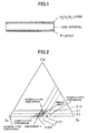
- the semiconductor crystal wafer was provided with, on the opposite surface thereof, an ohmic electrode of platinum by electroless plating (see Fig. 1).
- Composition of the In x Cd y Te z layer was analyzed by X-ray diffraction method (XRD) and energy distributed X-ray analysis device (EDX). As the result, the composition was determined as In 49.5 Cd 0.5 Te 50 (see Fig. 2). Thereafter, the wafer with electrodes was cut into chips having suitable size to produce a semiconductor radiation detector element of Schottky barrier.
- XRD X-ray diffraction method
- EDX energy distributed X-ray analysis device
- Fig. 3 schematically illustrates spectrum measurement operation using the radiation detector element.
- the platinum electrode negative pole
- the In x Cd y Te z electrode positive pole
- Fig. 4 is a graph illustrating change in response to radiation energy spectrum from 57 Co gamma radiation source with the time.
- reduction in performance of the detector element was evaluated by observing any change in peak channel response to 122 keV photoelectric absorption peak especially among photon energy emitted from the 57 Co gamma radiation source with the time.
- the CdTe radiation detector element of Schottky barrier type according to the present invention exhibited the constant response to the 122 keV photoelectric absorption event for period of 180 minutes after application of bias voltage.
- the radiation detector element of Schottky barrier type according to the present invention provided stable operation for longer period of time at room temperature.
- "Peak Channel Relative Value" at the ordinate in the graph of Fig. 4 was derived from such assumption that the value resulted immediately (or zero minute) after application of bias voltage is 1.
- a "P" type CdTe semiconductor crystal wafer having specific resistance of 10 9 ⁇ cm was provided with, on one surface thereof, a layer of compound of indium, cadmium and tellurium: In x Cd y Te z , as an electrode for forming Schottkey barrier, by resistance heating vapor deposition.
- the semiconductor crystal wafer was provided with, on the opposite surface thereof, an ohmic electrode of platinum by electroless plating (see Fig. 1).
- Composition of the In x Cd y Te z layer was analyzed by X-ray diffraction method (XRD) and energy distributed X-ray analysis device (EDX).
- the composition was determined as In 57.1 Cd 0 Te 42.9 (In 4 Te 3 ) (see Fig. 2).
- the CdTe radiation detector element of Schottky barrier type was used to form a spectrometer as in the case of Embodiment 1 and the response of the detector element to monochromatic radiation was observed.
- the radiation detector element of Embodiment 2 exhibited higher efficiency for charge collection and stable operation for longer period of time as in the case of Embodiment 1.
- a "P" type CdTe semiconductor crystal wafer having specific resistance of 10 9 ⁇ cm was provided with, on one surface thereof, a layer of compound of indium, cadmium and tellurium: In x Cd y Te z , as an electrode for forming Schottkey barrier, by resistance heating vapor deposition.
- the semiconductor crystal wafer was provided with, on the opposite surface thereof, an ohmic electrode of platinum by electroless plating (see Fig. 1).
- Composition of the In x Cd y Te z layer was analyzed by X-ray diffraction method (XRD) and energy distributed X-ray analysis device (EDX). As the result, the composition was determined as In 56.6 Cd 0.5 Te 42.9 (see Fig. 2).
- the CdTe radiation detector element of Schottky barrier type was used to conduct spectrum measurement as in the case of Embodiment 1 and the response of the detector element to monochromatic radiation was observed.
- the radiation detector element of Embodiment 3 exhibited higher efficiency for charge collection and stable operation for longer period of time as in the case of Embodiment 1.
- a CdTe semiconductor crystal wafer was provided with an indium layer on one surface thereof by sputtering, and it was provided with a platinum electrode on the opposite surface thereof (see Fig. 5).
- Composition of the indium layer was analyzed by X-ray diffraction method (XRD) and energy distributed X-ray analysis device (EDX).
- XRD X-ray diffraction method
- EDX energy distributed X-ray analysis device
- the layer was found to purely have indium (In 100 Cd 0 Te 0 ) (see Fig. 2).
- the radiation detector element fabricated in such manner exhibited Schottky characteristic, could be applied higher electric field, and provided higher efficiency of charge collection, as in the case of the embodiments as described above.
- the CdTe semiconductor radiation detector element rapidly lowered in performance with the time, as shown in Fig. 6.
- the photoelectric absorption peak channel response to 122 keV photon emitted from 57 Co gamma radiation source started to reduce only approx. 20 to 30 minutes after application of bias voltage, and then, lowered down to the value corresponding to approx. 90% of the initial value 50 minutes after application of bias voltage. Accordingly, the semiconductor radiation detector element in Example 1 provided no stable operation for certain time period. It is noted that "Peak Channel Relative Value" at the ordinate in the graph of Fig. 6 was derived from such assumption that the value resulted immediately (or zero minute) after application of bias voltage is 1.
- a CdTe semiconductor crystal wafer was provided with a layer of compound of indium, cadmium and tellurium, of which rate of occupation is represented by In 57.1 Cd 0.5 Te 42.4 , on one surface thereof by sputtering (see Fig. 2), and it was provided with a platinum electrode on the opposite surface thereof.
- the radiation detector element fabricated in such manner exhibited Schottky characteristic, could be applied higher electric field, and provided higher efficiency of charge collection, as in the case of the embodiments, as described above. However, the semiconductor radiation detector element rapidly lowered in performance with the time and provided no stable operation for certain time period, as in the case of Example 1.
- a CdTe semiconductor crystal wafer was provided with a layer of compound of indium, cadmium and tellurium, of which rate of occupation is represented by In 42.9 Cd 0 Te 57.1 (or In 3 Te 4 ), on one surface thereof by sputtering (see Fig. 2), and it was provided with a platinum electrode on the opposite surface thereof.
- the radiation detector element fabricated in such manner exhibited Schottky characteristic, could be applied higher electric field, and provided higher efficiency of charge collection, as in the case of the embodiments, as described above. However, the semiconductor radiation detector element rapidly lowered in performance with the time and provided no stable operation for certain time period, as in the case of Example 1.
- a CdTe semiconductor crystal wafer was provided with a layer of compound of indium, cadmium and tellurium, of which rate of occupation is represented by In 45.1 Cd 12 Te 42.9 , on one surface thereof by sputtering (see Fig. 2), and it was provided with a platinum electrode on the opposite surface thereof.
- the radiation detector element fabricated in such manner exhibited Schottky characteristic, could be applied higher electric field, and provided higher efficiency of charge collection, as in the case of the embodiments, as described above. However, the semiconductor radiation detector element rapidly lowered in performance with the time and provided no stable operation for certain time period, as in the case of Example 1.
Landscapes
- Light Receiving Elements (AREA)
- Measurement Of Radiation (AREA)
- Solid State Image Pick-Up Elements (AREA)
Abstract
Description
Claims (3)
- A semiconductor radiation detector element of Schottky barrier type, comprising: a compound semiconductor crystal including cadmium and tellurium as main components; and voltage application means for applying voltage to the compound semiconductor crystal, said voltage application means including a compound of indium, cadmium and tellurium: InxCdyTez formed on one surface of the compound semiconductor crystal.
- A semiconductor radiation detector element of Schottky barrier type according to claim 1 in which the rate "z" of occupation of tellurium in the compound of indium, cadmium and tellurium: InxCdyTez is within the range of not less than 42.9%, but not greater than 50% by ratio of number of atoms.
- A semiconductor radiation detector element of Schottky barrier type according to claim 1 in which the rate "y" of occupation of cadmium in the compound of indium, cadmium and tellurium: InxCdyTez is within the range of not less than 0%, but not greater than 10% by ratio of number of atoms.
Applications Claiming Priority (3)
| Application Number | Priority Date | Filing Date | Title |
|---|---|---|---|
| JP2001144313A JP5135651B2 (en) | 2001-05-15 | 2001-05-15 | Semiconductor radiation detector |
| JP2001144313 | 2001-05-15 | ||
| PCT/JP2002/003615 WO2002093654A1 (en) | 2001-05-15 | 2002-04-11 | Semiconductor radiation detecting element |
Publications (3)
| Publication Number | Publication Date |
|---|---|
| EP1391940A1 true EP1391940A1 (en) | 2004-02-25 |
| EP1391940A4 EP1391940A4 (en) | 2006-08-09 |
| EP1391940B1 EP1391940B1 (en) | 2007-11-07 |
Family
ID=18990280
Family Applications (1)
| Application Number | Title | Priority Date | Filing Date |
|---|---|---|---|
| EP02718533A Expired - Lifetime EP1391940B1 (en) | 2001-05-15 | 2002-04-11 | Semiconductor radiation detecting element |
Country Status (9)
| Country | Link |
|---|---|
| US (1) | US6975012B2 (en) |
| EP (1) | EP1391940B1 (en) |
| JP (1) | JP5135651B2 (en) |
| AT (1) | ATE377845T1 (en) |
| CA (1) | CA2447403C (en) |
| DE (1) | DE60223358T2 (en) |
| RU (1) | RU2281531C2 (en) |
| TW (1) | TW541708B (en) |
| WO (1) | WO2002093654A1 (en) |
Cited By (1)
| Publication number | Priority date | Publication date | Assignee | Title |
|---|---|---|---|---|
| EP2026383A2 (en) | 2007-08-17 | 2009-02-18 | CSEM Centre Suisse d'Electronique et de Microtechnique SA | X-Ray Imaging Device and Method for the Manufacturing thereof |
Families Citing this family (6)
| Publication number | Priority date | Publication date | Assignee | Title |
|---|---|---|---|---|
| CN102016639A (en) * | 2008-04-24 | 2011-04-13 | 住友重机械工业株式会社 | Semiconductor detector block and positron emission tomography device using the same |
| GB0908583D0 (en) | 2009-05-19 | 2009-06-24 | Durham Scient Crystals Ltd | Semiconductor device contacts |
| US8165266B2 (en) * | 2009-09-10 | 2012-04-24 | General Electric Company | Transverse scanning bone densitometer and detector used in same |
| DE102012215041A1 (en) * | 2012-08-23 | 2014-02-27 | Siemens Aktiengesellschaft | Method for producing a semiconductor element of a direct-converting X-ray detector |
| JP6433644B2 (en) * | 2013-06-07 | 2018-12-05 | シーメンス アクチエンゲゼルシヤフトSiemens Aktiengesellschaft | Semiconductor wafer dicing method |
| RU2578103C1 (en) * | 2014-11-10 | 2016-03-20 | Федеральное государственное казенное военное образовательное учреждение высшего профессионального образования "Военная академия Ракетных войск стратегического назначения имени Петра Великого" Министерства обороны Российской Федерации | Combined semiconductor receiver of electromagnetic emission |
Family Cites Families (14)
| Publication number | Priority date | Publication date | Assignee | Title |
|---|---|---|---|---|
| US4190486A (en) * | 1973-10-04 | 1980-02-26 | Hughes Aircraft Company | Method for obtaining optically clear, high resistivity II-VI, III-V, and IV-VI compounds by heat treatment |
| FR2336804A1 (en) * | 1975-12-23 | 1977-07-22 | Telecommunications Sa | IMPROVEMENTS MADE TO SEMICONDUCTOR DEVICES, ESPECIALLY TO PHOTOVOLTAIC DETECTORS INCLUDING A SUBSTRATE BASED ON A CDXHG1-XTE ALLOY, AND PROCESS FOR MANUFACTURING SUCH A PERFECTED DEVICE |
| JPS5630771A (en) * | 1979-08-20 | 1981-03-27 | Matsushita Electric Ind Co Ltd | Manufacture of photoreceptor |
| US4613495A (en) * | 1984-07-20 | 1986-09-23 | Hughes Aircraft Company | Growth of single crystal Cadmium-Indium-Telluride |
| JPS62115391A (en) * | 1985-11-13 | 1987-05-27 | Nippon Mining Co Ltd | Cdte radiant ray detector |
| SU1644637A1 (en) * | 1989-10-09 | 1996-09-20 | А.И. Поляков | X-ray radiation detector |
| JPH03248578A (en) * | 1990-02-27 | 1991-11-06 | Nikko Kyodo Co Ltd | Manufacture of semiconductor radioactive ray detecting element |
| SU1814399A1 (en) * | 1991-01-02 | 1996-09-20 | Научно-исследовательский институт импульсной техники | Detector of pulsed ionizing emission |
| US5510644A (en) * | 1992-03-23 | 1996-04-23 | Martin Marietta Corporation | CDTE x-ray detector for use at room temperature |
| US5391882A (en) * | 1993-06-11 | 1995-02-21 | Santa Barbara Research Center | Semiconductor gamma ray detector including compositionally graded, leakage current blocking potential barrier layers and method of fabricating the detector |
| US6030853A (en) * | 1993-08-13 | 2000-02-29 | Drs Fpa, L.P. | Method of producing intrinsic p-type HgCdTe using CdTe capping layer |
| JPH07221340A (en) * | 1994-01-31 | 1995-08-18 | Hitachi Chem Co Ltd | Semiconductor radiation detector |
| US6011264A (en) * | 1994-08-11 | 2000-01-04 | Urigal Technologies, Ltd. | Apparatus, system and method for gamma ray and x-ray detection |
| JP4397012B2 (en) * | 2001-11-05 | 2010-01-13 | 独立行政法人 宇宙航空研究開発機構 | Semiconductor image sensor having hole-type electrode and manufacturing method thereof |
-
2001
- 2001-05-15 JP JP2001144313A patent/JP5135651B2/en not_active Expired - Lifetime
-
2002
- 2002-04-11 EP EP02718533A patent/EP1391940B1/en not_active Expired - Lifetime
- 2002-04-11 CA CA2447403A patent/CA2447403C/en not_active Expired - Lifetime
- 2002-04-11 RU RU2003133302/28A patent/RU2281531C2/en active
- 2002-04-11 AT AT02718533T patent/ATE377845T1/en not_active IP Right Cessation
- 2002-04-11 WO PCT/JP2002/003615 patent/WO2002093654A1/en not_active Ceased
- 2002-04-11 DE DE60223358T patent/DE60223358T2/en not_active Expired - Lifetime
- 2002-05-06 TW TW091109369A patent/TW541708B/en not_active IP Right Cessation
-
2003
- 2003-10-29 US US10/697,129 patent/US6975012B2/en not_active Expired - Lifetime
Cited By (2)
| Publication number | Priority date | Publication date | Assignee | Title |
|---|---|---|---|---|
| EP2026383A2 (en) | 2007-08-17 | 2009-02-18 | CSEM Centre Suisse d'Electronique et de Microtechnique SA | X-Ray Imaging Device and Method for the Manufacturing thereof |
| US8237126B2 (en) | 2007-08-17 | 2012-08-07 | Csem Centre Suisse D'electronique Et De Mictrotechnique Sa | X-ray imaging device and method for the manufacturing thereof |
Also Published As
| Publication number | Publication date |
|---|---|
| CA2447403A1 (en) | 2002-11-21 |
| TW541708B (en) | 2003-07-11 |
| US20040129994A1 (en) | 2004-07-08 |
| RU2281531C2 (en) | 2006-08-10 |
| RU2003133302A (en) | 2005-03-20 |
| US6975012B2 (en) | 2005-12-13 |
| EP1391940B1 (en) | 2007-11-07 |
| DE60223358T2 (en) | 2008-08-28 |
| WO2002093654A1 (en) | 2002-11-21 |
| ATE377845T1 (en) | 2007-11-15 |
| DE60223358D1 (en) | 2007-12-20 |
| EP1391940A4 (en) | 2006-08-09 |
| JP5135651B2 (en) | 2013-02-06 |
| CA2447403C (en) | 2012-09-04 |
| JP2002344000A (en) | 2002-11-29 |
Similar Documents
| Publication | Publication Date | Title |
|---|---|---|
| Matsumoto et al. | Performance of a new Schottky CdTe detector for hard X-ray spectroscopy | |
| Overdick et al. | Status of direct conversion detectors for medical imaging with X-rays | |
| Bolotnikov et al. | Factors limiting the performance of CdZnTe detectors | |
| US9121953B2 (en) | Array of virtual Frisch-grid detectors with common cathode and reduced length of shielding electrodes | |
| US4692782A (en) | Semiconductor radioactive ray detector | |
| US6350989B1 (en) | Wafer-fused semiconductor radiation detector | |
| JP4037917B2 (en) | X-ray detection element and method of operating the element | |
| US9134439B2 (en) | Array of virtual Frisch-grid detectors with common cathode and reduced length of shielding electrodes | |
| US7161155B1 (en) | X-ray detector with increased detective quantum efficiency | |
| EP1357608B1 (en) | X-ray detector | |
| US7060523B2 (en) | Lithium-drifted silicon detector with segmented contacts | |
| JPH04251988A (en) | amorphous silicon sensor | |
| US6975012B2 (en) | Semiconductor radiation detector having voltage application means comprises InxCdyTez on CdTe semiconductor substrate | |
| US6011264A (en) | Apparatus, system and method for gamma ray and x-ray detection | |
| Amman et al. | Position-sensitive germanium detectors for gamma-ray imaging and spectroscopy | |
| Bolotnikov et al. | Large area/volume CZT nuclear detectors | |
| US20050184320A1 (en) | Photoconductor having an embedded contact electrode | |
| JPH01138486A (en) | Multichannel type semiconductor radiation detector | |
| US7002158B2 (en) | Solid-state radiation detector using a single crystal of compound semiconductor InSb | |
| JPH0690291B2 (en) | Radiation detector | |
| JPH07335927A (en) | Method of manufacturing semiconductor radiation detector | |
| KR100720610B1 (en) | Radiation detector | |
| Hammig et al. | Fabrication methods by which the intrinsic noise is reduced in Si and CZT nuclear radiation detectors | |
| Yoo et al. | Ultrafast molecular beam epitaxy (MBE) CdTe photoconductor array for synchrotron radiation | |
| JPS63182868A (en) | Radiation detection element |
Legal Events
| Date | Code | Title | Description |
|---|---|---|---|
| PUAI | Public reference made under article 153(3) epc to a published international application that has entered the european phase |
Free format text: ORIGINAL CODE: 0009012 |
|
| 17P | Request for examination filed |
Effective date: 20031106 |
|
| AK | Designated contracting states |
Kind code of ref document: A1 Designated state(s): AT BE CH CY DE DK ES FI FR GB GR IE IT LI LU MC NL PT SE TR |
|
| A4 | Supplementary search report drawn up and despatched |
Effective date: 20060712 |
|
| 17Q | First examination report despatched |
Effective date: 20061124 |
|
| GRAP | Despatch of communication of intention to grant a patent |
Free format text: ORIGINAL CODE: EPIDOSNIGR1 |
|
| RIC1 | Information provided on ipc code assigned before grant |
Ipc: H01L 31/032 20060101ALI20070330BHEP Ipc: H01L 31/0224 20060101ALI20070330BHEP Ipc: H01L 31/118 20060101AFI20070330BHEP |
|
| GRAS | Grant fee paid |
Free format text: ORIGINAL CODE: EPIDOSNIGR3 |
|
| GRAA | (expected) grant |
Free format text: ORIGINAL CODE: 0009210 |
|
| AK | Designated contracting states |
Kind code of ref document: B1 Designated state(s): AT BE CH CY DE DK ES FI FR GB GR IE IT LI LU MC NL PT SE TR |
|
| REG | Reference to a national code |
Ref country code: GB Ref legal event code: FG4D |
|
| REG | Reference to a national code |
Ref country code: IE Ref legal event code: FG4D |
|
| REG | Reference to a national code |
Ref country code: CH Ref legal event code: EP |
|
| REF | Corresponds to: |
Ref document number: 60223358 Country of ref document: DE Date of ref document: 20071220 Kind code of ref document: P |
|
| PG25 | Lapsed in a contracting state [announced via postgrant information from national office to epo] |
Ref country code: ES Free format text: LAPSE BECAUSE OF FAILURE TO SUBMIT A TRANSLATION OF THE DESCRIPTION OR TO PAY THE FEE WITHIN THE PRESCRIBED TIME-LIMIT Effective date: 20080218 Ref country code: SE Free format text: LAPSE BECAUSE OF FAILURE TO SUBMIT A TRANSLATION OF THE DESCRIPTION OR TO PAY THE FEE WITHIN THE PRESCRIBED TIME-LIMIT Effective date: 20080207 Ref country code: LI Free format text: LAPSE BECAUSE OF FAILURE TO SUBMIT A TRANSLATION OF THE DESCRIPTION OR TO PAY THE FEE WITHIN THE PRESCRIBED TIME-LIMIT Effective date: 20071107 Ref country code: NL Free format text: LAPSE BECAUSE OF FAILURE TO SUBMIT A TRANSLATION OF THE DESCRIPTION OR TO PAY THE FEE WITHIN THE PRESCRIBED TIME-LIMIT Effective date: 20071107 Ref country code: CH Free format text: LAPSE BECAUSE OF FAILURE TO SUBMIT A TRANSLATION OF THE DESCRIPTION OR TO PAY THE FEE WITHIN THE PRESCRIBED TIME-LIMIT Effective date: 20071107 |
|
| NLV1 | Nl: lapsed or annulled due to failure to fulfill the requirements of art. 29p and 29m of the patents act | ||
| REG | Reference to a national code |
Ref country code: CH Ref legal event code: PL |
|
| ET | Fr: translation filed | ||
| PG25 | Lapsed in a contracting state [announced via postgrant information from national office to epo] |
Ref country code: AT Free format text: LAPSE BECAUSE OF FAILURE TO SUBMIT A TRANSLATION OF THE DESCRIPTION OR TO PAY THE FEE WITHIN THE PRESCRIBED TIME-LIMIT Effective date: 20071107 |
|
| PG25 | Lapsed in a contracting state [announced via postgrant information from national office to epo] |
Ref country code: DK Free format text: LAPSE BECAUSE OF FAILURE TO SUBMIT A TRANSLATION OF THE DESCRIPTION OR TO PAY THE FEE WITHIN THE PRESCRIBED TIME-LIMIT Effective date: 20071107 |
|
| PG25 | Lapsed in a contracting state [announced via postgrant information from national office to epo] |
Ref country code: BE Free format text: LAPSE BECAUSE OF FAILURE TO SUBMIT A TRANSLATION OF THE DESCRIPTION OR TO PAY THE FEE WITHIN THE PRESCRIBED TIME-LIMIT Effective date: 20071107 |
|
| PLBE | No opposition filed within time limit |
Free format text: ORIGINAL CODE: 0009261 |
|
| STAA | Information on the status of an ep patent application or granted ep patent |
Free format text: STATUS: NO OPPOSITION FILED WITHIN TIME LIMIT |
|
| PG25 | Lapsed in a contracting state [announced via postgrant information from national office to epo] |
Ref country code: PT Free format text: LAPSE BECAUSE OF FAILURE TO SUBMIT A TRANSLATION OF THE DESCRIPTION OR TO PAY THE FEE WITHIN THE PRESCRIBED TIME-LIMIT Effective date: 20080407 |
|
| 26N | No opposition filed |
Effective date: 20080808 |
|
| PG25 | Lapsed in a contracting state [announced via postgrant information from national office to epo] |
Ref country code: MC Free format text: LAPSE BECAUSE OF NON-PAYMENT OF DUE FEES Effective date: 20080430 |
|
| PG25 | Lapsed in a contracting state [announced via postgrant information from national office to epo] |
Ref country code: GR Free format text: LAPSE BECAUSE OF FAILURE TO SUBMIT A TRANSLATION OF THE DESCRIPTION OR TO PAY THE FEE WITHIN THE PRESCRIBED TIME-LIMIT Effective date: 20080208 |
|
| PG25 | Lapsed in a contracting state [announced via postgrant information from national office to epo] |
Ref country code: IE Free format text: LAPSE BECAUSE OF NON-PAYMENT OF DUE FEES Effective date: 20080411 |
|
| PG25 | Lapsed in a contracting state [announced via postgrant information from national office to epo] |
Ref country code: CY Free format text: LAPSE BECAUSE OF FAILURE TO SUBMIT A TRANSLATION OF THE DESCRIPTION OR TO PAY THE FEE WITHIN THE PRESCRIBED TIME-LIMIT Effective date: 20071107 |
|
| PG25 | Lapsed in a contracting state [announced via postgrant information from national office to epo] |
Ref country code: LU Free format text: LAPSE BECAUSE OF NON-PAYMENT OF DUE FEES Effective date: 20080411 |
|
| PG25 | Lapsed in a contracting state [announced via postgrant information from national office to epo] |
Ref country code: TR Free format text: LAPSE BECAUSE OF FAILURE TO SUBMIT A TRANSLATION OF THE DESCRIPTION OR TO PAY THE FEE WITHIN THE PRESCRIBED TIME-LIMIT Effective date: 20071107 |
|
| REG | Reference to a national code |
Ref country code: FR Ref legal event code: PLFP Year of fee payment: 15 |
|
| REG | Reference to a national code |
Ref country code: FR Ref legal event code: PLFP Year of fee payment: 16 |
|
| REG | Reference to a national code |
Ref country code: FR Ref legal event code: PLFP Year of fee payment: 17 |
|
| PGFP | Annual fee paid to national office [announced via postgrant information from national office to epo] |
Ref country code: DE Payment date: 20210420 Year of fee payment: 20 Ref country code: FR Payment date: 20210423 Year of fee payment: 20 Ref country code: FI Payment date: 20210421 Year of fee payment: 20 Ref country code: IT Payment date: 20210427 Year of fee payment: 20 |
|
| PGFP | Annual fee paid to national office [announced via postgrant information from national office to epo] |
Ref country code: GB Payment date: 20210421 Year of fee payment: 20 |
|
| REG | Reference to a national code |
Ref country code: DE Ref legal event code: R071 Ref document number: 60223358 Country of ref document: DE |
|
| REG | Reference to a national code |
Ref country code: GB Ref legal event code: PE20 Expiry date: 20220410 |
|
| REG | Reference to a national code |
Ref country code: FI Ref legal event code: MAE |
|
| PG25 | Lapsed in a contracting state [announced via postgrant information from national office to epo] |
Ref country code: GB Free format text: LAPSE BECAUSE OF EXPIRATION OF PROTECTION Effective date: 20220410 |