EP1391937A2 - Method for improving a semiconductor substrate having SiGe film and semiconductor device manufactured by using this method - Google Patents
Method for improving a semiconductor substrate having SiGe film and semiconductor device manufactured by using this method Download PDFInfo
- Publication number
- EP1391937A2 EP1391937A2 EP03018848A EP03018848A EP1391937A2 EP 1391937 A2 EP1391937 A2 EP 1391937A2 EP 03018848 A EP03018848 A EP 03018848A EP 03018848 A EP03018848 A EP 03018848A EP 1391937 A2 EP1391937 A2 EP 1391937A2
- Authority
- EP
- European Patent Office
- Prior art keywords
- sige
- film
- ion implantation
- implanted
- substrate
- Prior art date
- Legal status (The legal status is an assumption and is not a legal conclusion. Google has not performed a legal analysis and makes no representation as to the accuracy of the status listed.)
- Withdrawn
Links
Images




Classifications
-
- H—ELECTRICITY
- H10—SEMICONDUCTOR DEVICES; ELECTRIC SOLID-STATE DEVICES NOT OTHERWISE PROVIDED FOR
- H10P—GENERIC PROCESSES OR APPARATUS FOR THE MANUFACTURE OR TREATMENT OF DEVICES COVERED BY CLASS H10
- H10P36/00—Gettering within semiconductor bodies
-
- H—ELECTRICITY
- H10—SEMICONDUCTOR DEVICES; ELECTRIC SOLID-STATE DEVICES NOT OTHERWISE PROVIDED FOR
- H10P—GENERIC PROCESSES OR APPARATUS FOR THE MANUFACTURE OR TREATMENT OF DEVICES COVERED BY CLASS H10
- H10P30/00—Ion implantation into wafers, substrates or parts of devices
- H10P30/20—Ion implantation into wafers, substrates or parts of devices into semiconductor materials, e.g. for doping
- H10P30/202—Ion implantation into wafers, substrates or parts of devices into semiconductor materials, e.g. for doping characterised by the semiconductor materials
- H10P30/204—Ion implantation into wafers, substrates or parts of devices into semiconductor materials, e.g. for doping characterised by the semiconductor materials into Group IV semiconductors
-
- H—ELECTRICITY
- H10—SEMICONDUCTOR DEVICES; ELECTRIC SOLID-STATE DEVICES NOT OTHERWISE PROVIDED FOR
- H10D—INORGANIC ELECTRIC SEMICONDUCTOR DEVICES
- H10D30/00—Field-effect transistors [FET]
- H10D30/60—Insulated-gate field-effect transistors [IGFET]
- H10D30/751—Insulated-gate field-effect transistors [IGFET] having composition variations in the channel regions
-
- H—ELECTRICITY
- H10—SEMICONDUCTOR DEVICES; ELECTRIC SOLID-STATE DEVICES NOT OTHERWISE PROVIDED FOR
- H10P—GENERIC PROCESSES OR APPARATUS FOR THE MANUFACTURE OR TREATMENT OF DEVICES COVERED BY CLASS H10
- H10P30/00—Ion implantation into wafers, substrates or parts of devices
- H10P30/20—Ion implantation into wafers, substrates or parts of devices into semiconductor materials, e.g. for doping
- H10P30/208—Ion implantation into wafers, substrates or parts of devices into semiconductor materials, e.g. for doping of electrically inactive species
Definitions
- the present invention relates to a method for improving a semiconductor substrate having a SiGe film wherein the quality of the SiGe film is improved in regard to the surface condition, to the crystallinity and to relaxation of lattice distortion in the semiconductor substrate wherein the SiGe film is formed on a Si or SOI substrate, further, it relates to a semiconductor device manufactured by using a semiconductor substrate of which the quality has been improved.
- a method is known wherein a distorted SiGe film having a lattice constant differing from that of Si is formed on a Si substrate in a virtual lattice form and the distortion caused within this SiGe film by the mismatch between the lattice constants of Si and SiGe is relieved through the introduction of misfit dislocations and, after that, an upper layer Si film is formed on the SiGe film as a cap layer in order to improve the mobility of electrons and holes that pass through channel regions.
- This upper layer Si film is stretched by the SiGe film having a lattice constant that is greater than the Si film and, thereby, distortion is caused within the upper layer Si film and thus, the band structure is altered so as to improve carrier mobility.
- a method for relaxing the distortion in a SiGe film wherein the thickness of the SiGe film is increased and thereby, the elastic strain energy of the SiGe film is increased so as to relax the lattice. It has been reported, for example, that by gradually increasing the Ge concentration in a SiGe film in order to form a SiGe film having a concentration gradient of approximately 1 ⁇ m, relaxation of distortion in the SiGe film can be achieved in the paper in Appl. Phys. Lett. 59 (13), 1611 (1991) by Y. J. Mii, et al.
- a method for relaxing the distortion in a thin SiGe film formed on a Si substrate wherein an ion implantation process, such as of hydrogen, is carried out on the thin SiGe film and, after that, an annealing process is carried out at a high temperature so that layered defects that have been created in defect layers within the Si substrate cause slippage and, therefore, misfit dislocations are generated at the interface of SiGe/Si.
- an ion implantation process such as of hydrogen
- the SiGe film exceeds the critical film thickness needed to gain perfect crystallinity of the SiGe film and, therefore, a very great number of defects occur in the SiGe film.
- the film grows while distortion is relaxed by itself and, therefore, roughness, referred to as cross hatching, occurs at intervals of several tens of ⁇ m on the surface of the SiGe film such that the film cannot be used as it is as a semiconductor substrate and, therefore, a flattening process, such as a CMP process, becomes essential and another SiGe film must be grown on the surface of the SiGe film on the substrate on which the flattening process has been carried out.
- a flattening process such as a CMP process
- R indicates the relaxation ratio of lattice distortion in the SiGe film
- a // (Si) and a // (SiGe) are the (001) lattice constants of Si and of SiGe, respectively, in the condition of complete lattice relaxation and a // (x) is the (001) lattice constant of the actually measured SiGe layer.
- the present invention is aimed to provide a method for determining the relationship between the film condition of a thin SiGe film and the hydrogen ion implantation condition for the achievement of a sufficient distortion relaxation ratio, of a good crystallinity and of a good surface condition in regard to the SiGe film formed on a Si or SOI substrate so that good conditions for enabling the improvement of quality of the SiGe film on the Si or SOI substrate can be determined.
- a method for improving a semiconductor substrate having a SiGe film on a Si or SOI substrate by using a hydrogen ion implantation and an annealing comprising the steps of:
- This method for improving quality utilizes the results of an examination of the relationship between the conditions of the SiGe film formed on a Si or SOI substrate and the conditions of hydrogen ion implantation as well as, in particular, the results of an empirical examination carried out to determine which parameters among the conditions of the SiGe film and conditions for hydrogen ion implantation affect the surface condition, the crystallinity and distortion relaxation ratio.
- the crystallinity and the distortion relaxation ratio can effectively be represented using three parameters: elastic strain energy U SiGe empirically calculated from the Ge concentration and the film thickness of the SiGe film; the peak depth Rp, which 'is the distance between the SiGe/Si interface and the peak position of the hydrogen ion concentration in the Si calculated from the hydrogen ion implantation energy and the film thickness of the SiGe film: and the amount of implanted hydrogen ions.
- data representing the range of the conditions appropriate for improving quality using these three parameters is determined in advance, and selecting the desired improvement condition from said range, and determining an amount of hydrogen ions to be implanted and a hydrogen ion implantation energy.
- the present invention achieves an improvement in the quality of the surface condition, crystallinity and relaxation of lattice distortion of a SiGe film by implementing a hydrogen ion implantation and an annealing on a semiconductor substrate formed of the SiGe film on a Si substrate or on an SOI substrate.
- a semiconductor substrate formed of a SiGe film on a Si substrate or on an SOI substrate is used.
- Si substrate though a single crystal Si substrate is preferable, other Si substrates, such as a polycrystal Si substrate may be used as long as a SiGe film can be grown on the substrate in a heteroepitaxial manner.
- any SOI substrate may be used in the same manner as long as a SiGe film can be grown on the Si layer on the SOI substrate in an epitaxial manner.
- the SiGe film may be formed in any type of unit as long as the SiGe film is a heteroepitaxially grown film formed on Si and, for example, a SiGe film having a desired Ge concentration and having a desired film thickness can be formed in a low pressure chemical vapor deposition unit (LPCVD) that utilize silane gas (SiH4) and germane gas (GeH4) as material gases.
- LPCVD low pressure chemical vapor deposition unit
- the hydrogen ion implantation is carried out using a known ion implantation unit. At this time at least the amount of implemented hydrogen ions (dose) and the hydrogen ion implantation energy can be appropriately altered as parameters for ion implantation.
- the annealing after the hydrogen ion implantation is carried out using a heat processing furnace wherein the introduction of atmospheric gases such as nitrogen, hydrogen and argon is possible.
- the annealing temperature is preferably about 700°C to about 900°C and it is preferable to carry out the annealing at, for example, about 800°C.
- the surface condition of the SiGe film of which the quality has been improved according to the present invention is observed using a Nomarski microscope in order to determine the quality according to the existence of local peeling or cross hatching.
- the quality of the crystallinity and the distortion relaxation ratio is determined by carrying out an X-ray diffraction (XRD) analysis.
- the elastic strain energy and the the peak depth Rp which is the distance between the SiGe/Si interface and the peak position of the hydrogen ion concentration in the Si, used for representing the range of the predetermined appropriate conditions for quality improvement are described.
- a SiGe film (Ge concentration; x, thickness of SiGe film; h) in the condition of complete lattice match with a Si substrate has an elastic strain energy per unit area (normalized elastic strain energy as described below) found according to the following equation [2].
- U SiGe is the elastic strain energy of a SiGe film per unit area
- ⁇ is the Poisson's ratio of SiGe
- E is the Young's modulus
- ⁇ // is the amount of distortion in (001) SiGe lattice.
- the elastic strain energy of a Ge film in the condition wherein the Ge film made of 100% Ge with a film thickness of 100 nm is in the state of complete lattice match with a Si substrate, is assumed to be 1 and the normalized elastic strain energy of the SiGe film is assumed to be the normalized elastic strain energy U SiGe for the purpose of convenience in the following description.
- the peak depth Rp which is defined as the distance between the position of the peak concentration of the implemented hydrogen ions and the SiGe/Si interface, is uniformly determined by the film thickness of the SiGe film and by the ion implantation energy.
- the peak position of the hydrogen ions at the time of implantation using an ion implantation energy of 25 KeV is located, for example, at a position 250 nm from the surface of the substrate and the peak depth Rp is 50 nm from the SiGe/Si interface in the case wherein the film thickness of SiGe is 200 nm.
- the range of appropriate quality improvement conditions is represented using the three parameters: the normalized elastic strain energy U SiGe ; the the peak depth Rp; and the amount of hydrogen ion implantation
- the range can be represented according to the X-Y coordinate system wherein two parameters out of the three parameters are indicated along the X and Y coordinate axes while the remaining parameter is used as a sub-parameter, which is fixed at any of a plurality of appropriate values.
- the normalized elastic strain energy U SiGe and the the peak depth Rp for example, are indicated along the X-Y coordinates and the amount of ion implantation is fixed at an appropriate value as a sub-parameter.
- the range of appropriate quality improvement conditions may be represented according to a three-dimensional coordinate system wherein the three parameters: the normalized elastic strain energy U SiGe ; the peak depth Rp; and the amount of ion implantation, are used as the X-Y-Z coordinate axes.
- the pair of numeric values (Rp, U SiGe ) of elastic strain energy U SiGe and the the peak depth Rp becomes quality improvement condition selection parameters while the amount of ion implantation becomes a sub-parameter.
- the range of the appropriate quality improvement condition selection parameter is empirically found for every amount of hydrogen ion implantation (2 ⁇ 10 16 H + /cm 2 , 3 x 10 16 H + /cm 2 , 4 x 10 16 H + / cm 2 , for example) so that an Rp- U SiGe graph having Rp and U SiGe as the coordinate axes is prepared and, thereby, the range of (Rp, U SiGe ) for the appropriate quality improvement conditions is determined.
- the amount of hydrogen ion implantation is set at, for example, 3 ⁇ 10 16 H + / cm 2 for the SiGe film having a Ge concentration and a film thickness wherein the normalized elastic strain energy U SiGe is in a range of, for example, not less than 0.09 and less than 0.1 while the energy of hydrogen ion implantation is varied so that a plurality of ion implantations having differing peak depths Rp is carried out and the distortion relaxation ratio, crystallinity and the surface condition of the respective SiGe films are analyzed and, thereby, data is acquired concerning the appropriate range at which the the peak depth Rp should be set in order to implement a sufficient relaxation ratio, an appropriate crystallinity and an appropriate surface condition.
- a sufficient relaxation ratio, an appropriate crystallinity and an appropriate surface condition can be implemented in the case wherein the peak depth Rp is in a range of, for example, 33 nm to 75 nm.
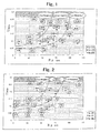
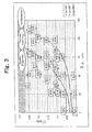
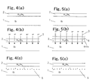
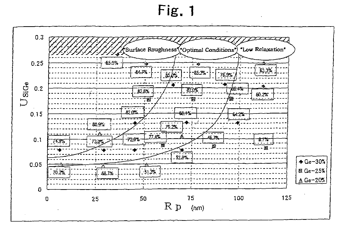
- Fig. 1 to 3 are Rp-U SiGe graphs showing ranges of appropriate quality improvement conditions defined according to the above described method.
- Fig. 1 shows a case wherein the amount of implanted hydrogen ions, which is a sub-parameter, is 3 ⁇ 10 16 H + /cm 2
- Fig. 2 shows a case wherein the amount of implanted hydrogen ions is 2 ⁇ 10 16 H + /cm 2
- Fig. 3 shows a case wherein the amount of implanted hydrogen ions is 4 ⁇ 10 16 H + /cm 2 .
- (Rp, U SiGe ) in the area shown as the "optimal condition” area provides a SiGe film having an excellent surface condition, crystallinity and distortion relaxation ratio
- the film thickness exceeds the critical film thickness for gaining a complete crystal of the SiGe film and, therefore, many defects occur in the SiGe film and the crystallinity becomes poor.
- the SiGe film grows while relaxing its own distortion and, thereby, roughness at intervals of several tens of ⁇ m, which is referred to as cross hatching, occurs on the surface of the film. Accordingly, the range wherein the normalized elastic energy exceeds 0.266 is excluded under all conditions.
- the range of elastic strain energy U SiGe for excellent quality improvement conditions is not greater than 0.266 in the present invention.
- the interface between the "surface roughening" area and the "optimal condition” area as well as the interface between the "optimal condition” area and the “low relaxation” area are formed of smooth curves, respectively.
- the interface between the "surface roughening" area and the "optimal condition” area is formed of a curve that passes (25 nm, 0.085), (43 nm, 0.120) and (62 nm, 0.200) and the interface between the "optimal condition” area and the "low relaxation” area is formed of a curve that passes (25 nm, 0.050), (50 nm, 0.063) and (75 nm, 0.095).
- the interface between the "surface roughening" area and the "optimal condition” area is formed of a curve that passes (25 nm, 0.117), (50 nm, 0.170) and (60 nm, 0.240) and the interface between the "optimal condition” area and the "low relaxation” area is formed of a curve that passes (25 nm, 0.082), (50 nm, 0.107) and (75 nm, 0.170) .
- the interface between the "surface roughening" area and the "optimal condition” area is formed of a curve that passes (25 nm, 0.046), (50 nm, 0.097) and (75 nm, 0.190) and the interface between the "optimal condition” area and the "low relaxation” area is formed of a curve that passes (25 nm, 0.028), (50 nm, 0.037) and (75 nm, 0.067).
- the normalized elastic strain energy U SiGe is calculated according to formula 2 from the Ge concentration and the film thickness of the SiGe film on which quality improvement is carried out by means of hydrogen ion implantation.
- the energy for hydrogen ion implantation and the amount of implanted hydrogen ions, which are set as ion implantation conditions, are provisionally set.
- the peak depth Rp is calculated from this provisionally set energy for hydrogen ion implantation and from the film thickness of the SiGe film so that the quality improvement condition selection parameters (Rp, U SiGe ) are determined from the calculated U SiGe and Rp.
- these quality improvement condition selection parameters (Rp, U SiGe ) and the range of (Rp, U SiGe ) for excellent quality improvement conditions of the Rp-U SiGe graph corresponding to the provisionally set amount of implanted ions are compared so as to determine whether or not the quality improvement condition selection parameters (Rp, U SiGe ) are in the range of the excellent quality improvement condition selections.
- these conditions for hydrogen ion implantation are determined to be excellent quality improvement conditions and, thereby, the provisionally set energy for hydrogen ion implantation and amount of implanted hydrogen ions are determined as the conditions for ion implantation.
- an appropriate range of ion implantation conditions made up of the energy for ion implantation and the amount of implanted hydrogen ions can be determined in regard to the conditions, for the SiGe film, the conditions being made up of the Ge concentration and the film thickness of the SiGe film.
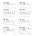
- Figs. 4 (a) to (c) are diagrams showing the steps of a method for improving the quality of a semiconductor substrate according to Embodiment 1 of the present invention.
- a Si substrate 1 was prepared. A pretreatments sulfuric acid boiling and SC-2 washing were carried out and a natural oxide film on the surface of the substrate was removed using diluted (5%) fluoric acid. Then, a semiconductor substrate was prepared wherein SiGe film 2, of which the quality was to be improved, was formed on the Si substrate 1 using a low pressure chemical vaporization unit (LPCVD) (Fig. 4(a)). The Ge concentration and the film thickness of this SiGe film 2 are determined according to the known film formation conditions. The Ge concentration and the film thickness of this SiGe film 2 were used for the calculation of Rp and U SiGe .
- LPCVD low pressure chemical vaporization unit
- Implantation conditions at this time were determined in reference to the Rp-U SiGe graph for each amount of implanted hydrogen ions that had been gained in advance through experiment (see Figs. 1 to 3).
- the amount of implanted hydrogen ions, from among ion implantation conditions was provisionally set (provisionally set at 3 ⁇ 10 16 H + /cm 2 , for example) and the Rp-U SiGe graph of the corresponding amount of implanted hydrogen ions (Fig. 1 in the case that the amount was provisionally set at 3 ⁇ 10 16 H + /cm 2 ), from among a plurality of Rp-U SiGe graphs prepared for every amount of implanted hydrogen ions, was referred to.
- the normalized elastic strain energy U SiGe was calculated according to the formula [2] from the Ge concentration and the film thickness of the SiGe film, of which the quality was to be improved, and the quality improvement condition selection parameters (Rp, U SiGe ) within the appropriate range for quality improvement conditions corresponding to the above value of U SiGe was extracted from the Rp-U SiGe graph so that the value of the energy for ion implantation was inversely calculated from this Rp value and from the film thickness of the SiGe film.
- the provisionally set value of the amount of implanted hydrogen ions is changed to another value and the reference Rp-U SiGe graph is changed so that the value of the energy for hydrogen ion implantation is inversely calculated according to the same procedure when a change in the ion implantation energy is desired.
- the amount of implanted hydrogen ions and the energy for hydrogen ion implantation that had been set as described above were determined as the ion implantation conditions and ion implantation was carried out according to such implantation conditions (Fig. 4(b)).
- the semiconductor substrate on which ion implantation had been carried out was annealed at 800°C for 10 minutes using a furnace in a nitrogen atmosphere so that microscopic holes, referred to as microcavities 9, were created in the vicinity of Rp (see Fig. 8).
- the layered defects generated by these microscopic holes caused slippage leading to misfit dislocations at the SiGe/Si interface and, thereby, lattice relaxation was able to be achieved (Fig. 4(c)).
- a first SiGe film having a Ge concentration of 24.1 % was epitaxially grown using a low pressure chemical vapor deposition (LPCVD) unit at 500°C so as to have a film thickness of 304 nm and to have a virtual lattice form from germane (GeH 4 ) and silane (SiH 4 ) material gases on a p type silicon (100) substrate wherein as pretreatments, sulfuric acid boiling and SC-2 washing had been carried out and a natural oxide film on the surface of the substrate had been removed using dilute (5 %) fluoric acid.
- LPCVD low pressure chemical vapor deposition
- the normalized elastic strain energy of the SiGe film was 0.177, which was equal to or smaller than the critical film thickness (that is to say, the normalized elastic strain energy was 0.266, or less), and the surface of the SiGe film immediately after growth was very clean, as shown in Fig. 9, wherein surface roughness referred to as cross hatching was not observed.
- a first SiGe film having a Ge concentration of 29.8 % was epitaxially grown in a virtual lattice form so as to have a film thickness of 321 nm at 500°C with the same pretreatment conditions as in Comparison Example 1.
- the normalized elastic strain energy of the SiGe film was 0.285, which exceeded the critical film thickness.
- surface roughness which is referred to as cross hatching, was observed to be significant on the surface of the SiGe film immediately after the SiGe film had been grown, as shown in Fig. 10.
- Fig. 1 is an Rp-U SiGe graph in the case wherein the amount of implanted ions was 3 ⁇ 10 16 H + /cm 2 .
- a hydrogen ion implantation in an amount (dose) of implanted hydrogen ions of 3 ⁇ 10 16 H + /cm 2 was carried out at a tilt angle of 7° using an implantation energy of 32 KeV on a SiGe/Si substrate having a Ge concentration of 24.1 %, having a film thickness of 304 nm and having distortion, which had been formed according to the conditions of Comparison Example 1, that is to say, in the condition wherein no surface roughness had been caused on the SiGe film.
- the substrate in which hydrogen ions had been implanted was annealed at 800°C for 10 minutes using a furnace in an N 2 atmosphere so as to generate microcavities 9 in the vicinity of Rp as shown in Fig. 8 and, thereby, the generated layered defects caused slippage so that misfit dislocations occured in the SiGe/Si interface and lattice relaxation occured.
- a first SiGe film having a Ge concentration of 28.8 % was epitaxially grown, using a low pressure chemical vapor deposition (LPCVD) unit at 500°C so as to have a film thickness of 158 nm and to have a virtual lattice form, from germane (GeH 4 ) and silane (SiH 4 ) material gases on a p type silicon (100) substrate on which the same pretreatments as in Comparison Examples 1 to 3 had been carried out.
- LPCVD low pressure chemical vapor deposition
- the normalized elastic strain energy of the SiGe film at this time was 0.131, which was equal to or smaller than the critical film thickness (that is to say, the normalized elastic strain energy was 0.266, or less).
- a hydrogen ion implantation resulting in an amount of implanted hydrogen ions of 3 ⁇ 10 16 H + /cm 2 was carried out on this distorted SiGe/ Si substrate using an implantation energy of 18 KeV at a tilt angle of 7°.
- the peak depth Rp of the hydrogen ions under such implantation conditions is located at a position in the Si substrate 72 nm away from the SiGe/Si interface according to the Monte Carlo simulation as described above (see Fig. 12).
- the substrate in which the hydrogen ions had been implanted was annealed at 800°C for 10 minutes using a furnace in an N 2 atmosphere.
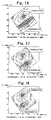
- Fig. 20 shows the SiGe/Si interface at this time. Microcavities did not significantly grow in the SiGe/Si interface under such implantation conditions. It was found according to XRD analysis of the (224) surface of the SiGe film, of which the distortion had been relaxed according to the above described implantation conditions, that the SiGe film had been sufficiently relaxed with the relaxation ratio of 80.1 % and had a good crystallinity as shown in Fig. 17.
- a first SiGe film having a Ge concentration of 23.6 % was epitaxially grown using a low pressure chemical vapor deposition (LPCVD) unit at 500°C so as to have a film thickness of 143 nm and to have a virtual lattice form from germane (GeH 4 ) and silane (SiH 4 ) material gases on a p type silicon (100) substrate, on which the same pretreatments as in Comparison Examples 1 to 3 and in Example 1 had been carried out.
- LPCVD low pressure chemical vapor deposition
- the normalized elastic strain energy of the SiGe film at this time was 0.079, which was equal to or smaller than the critical film thickness (that is to say, the normalized elastic strain energy was 0.266, or less).
- a hydrogen ion implantation in an amount of implanted hydrogen ions of 3 ⁇ 10 16 H + / cm 2 was carried out on this distorted SiGe/Si substrate using an implantation energy of 21 KeV at a tilt angle of 7°.
- the peak depth Rp of the hydrogen ions under such implantation conditions is located at a position in the Si substrate 114 nm away from the SiGe/Si interface according to the Monte Carlo simulation (see Fig. 12).
- the substrate in which the hydrogen ions had been implanted was annealed at 800°C for 10 minutes using a furnace in an N 2 atmosphere.
- (Rp, U SiGe ) is a point ( 114 nm, 0.079) in the Rp-U SiGe graph of Fig. 1, which is located at a position within the "low relaxation" region.
- the relaxation ratio of the SiGe film was, however, shown to be only 8.7 % in Fig. 18 according to XRD analysis of the (224) surface of the SiGe film wherein the distortion had been relaxed.
- Fig. 1 is the Rp-U SiGe graph in the case wherein the amount of implanted ions was 2 ⁇ 10 16 H + / cm 2 .
- a first SiGe film having a Ge concentration of 28.8 % was epitaxially grown using a low pressure chemical vapor deposition (LPCVD) unit at 500°C so as to have a film thickness of 248 nm to have a virtual lattice form from germane (GeH 4 ) and silane (SiH 4 ) material gases on a p type silicon (100) substrate wherein as pretreatments, sulfuric acid boiling and SC-2 washing had been carried out and the natural oxide film on the surface of the substrate had been removed using dilute (5 %) fluoric acid.
- LPCVD low pressure chemical vapor deposition
- the normalized elastic strain energy of the SiGe film was 0.206, which was equal to or smaller than the critical film thickness (that is to say, the normalized elastic strain energy was 0.266, or less).
- the peak depth Rp of the hydrogen ions is located in the Si substrate 43 nm away from the SiGe/Si interface according to the Monte Carlo simulation (see Fig. 12).
- This substrate into which hydrogen ions had been implanted was annealed at 800°C for 10 minutes using a furnace in an N 2 atmosphere.
- (Rp, U SIGe ) is a point (43 nm, 0.206) in the Rp-U SiGe graph of Fig. 2, which is located at a position within the "surface roughening" region that is closer to the SiGe/Si interface than is "optimal condition" region.
- the relaxation ratio of the SiGe film was 85.5 % indicating a sufficient relaxation while the crystallinity was very poor according to XRD analysis of the (224) surface of the SiGe film of which the distortion had been relaxed according to the above described condition.
- a first SiGe film in a virtual lattice form was epitaxially grown at 500°C so as to have a Ge concentration of 28.8 % and so as to have a film thickness of 248 nm on a p type silicon (100) substrate wherein the same pretreatments as in Comparison Example 5 had been carried out.
- a hydrogen ion implantation was carried out on this distorted SiGe/Si substrate under the conditions wherein the implantation energy was 27 KeV, the amount of implanted hydrogen ions (dose) was 2 ⁇ 10 16 H + /cm 2 and the angle of tilt was 7°.
- the peak depth Rp of the hydrogen ions is located in the Si substrate 65 nm away from the SiGe/Si interface according to the Monte Carlo simulation (see Fig. 12).
- the substrate into which hydrogen ions had been implanted was annealed at 800°C for 10 minutes using a furnace in an N 2 atmosphere.
- (Rp, U SiGe ) is a point (65 nm, 0.206) in the Rp-U SiGe graph of Fig. 2, which is located at a position within the "optimal condition" region.
- a distorted SiGe/Si substrate was formed by epitaxially growing a similar SiGe film to that of Comparison Example 5 and of Example 2 on a substrate wherein similar pretreatments to those of Comparison Example 5 and of Example 2 had been carried out and a hydrogen ion implantation was carried out on this distorted SiGe/Si substrate under the conditions wherein the implantation energy was 30 KeV, the amount of implanted hydrogen ions (dose) was 2 ⁇ 10 16 H + /cm 2 and the angle of tilt is 7°.
- the peak depth Rp of the hydrogen ions under this implantation condition is at a position in the Si substrate 93 nm away from the SiGe/Si interface according to the Monte Carlo simulation (see Fig. 12) .
- the substrate into which hydrogen ions had been implanted was annealed at 800°C for 10 minutes using a furnace in an N 2 atmosphere.
- (Rp, U SiGe ) is a point (93 nm, 0.206) in the Rp-U SiGe graph of Fig. 2, which is located at a position within the "low relaxation" region.
- the relaxation ratio of the SiGe film was only 52.1 % indicating an insufficient relaxation according to XRD analysis of the (224) surface of the SiGe film of which the distortion had been relaxed according to the above described condition.
- Fig. 3 that is the Rp-U SiGe graph in the case wherein the amount of implanted ions is 4 ⁇ 10 16 H + /cm 2 .
- a first SiGe film having a Ge concentration of 19.4 % was epitaxially grown using a low pressure chemical vapor deposition (LPCVD) unit at 500°C so as to have a film thickness of 300 nm and to have a virtual lattice form from germane (GeH 4 ) and silane (SiH 4 ) material gases on a p type silicon (100) substrate wherein as pretreatments, sulfuric acid boiling and SC-2 washing had been carried out and the natural oxide film on the surface of the substrate had been removed using dilute (5 %) fluoric acid.
- LPCVD low pressure chemical vapor deposition
- the normalized elastic strain energy of the SiGe film was 0.113, which was equal to or smaller than the critical film thickness (that is to say the normalized elastic strain energy was 0.266, or less).
- the peak depth Rp of the hydrogen ions is located in the Si substrate 27 nm away from the SiGe/Si interface according to the Monte Carlo simulation (see Fig. 12).
- this substrate into which hydrogen ions had been implanted was annealed at 800°C for 10 minutes using a furnace in an N 2 atmosphere.
- (Rp, U SiGe ) is a point (27 nm, 0.113) in the Rp-U SiGe graph of Fig. 3, which is located at a position within the "surface roughening" region that is closer to the SiGe/Si interface than is "optimal condition" region.
- the relaxation ratio of the SiGe film was 85.3 % indicating a sufficient relaxation while the crystallinity was very poor according to XRD analysis of the (224) surface of the SiGe film of which the distortion had been relaxed according to the above described condition.
- a distorted SiGe/Si substrate was formed by epitaxially growing a similar SiGe film to that of Comparison Example 7 on a substrate wherein a similar pretreatments to that of Comparison Example 7 had been carried out and hydrogen ion implantation was carried out on this distorted SiGe/Si substrate under the conditions wherein the implantation energy was 33 KeV, the amount of implanted hydrogen ions (dose) was 4 ⁇ 10 16 H + /cm 2 and the angle of tilt was 7°.
- the peak depth Rp of the hydrogen ions under this implantation condition is at a position in the Si substrate 71 nm away from the SiGe/Si interface according to the Monte Carlo simulation (see Fig. 12).
- the substrate into which hydrogen ions had been implanted was annealed at 800°C for 10 minutes using a furnace in an N 2 atmosphere.
- (Rp, U SiGe ) is a point (71 nm, 0.113) in the Rp-U SiGe graph of Fig. 3, which is located at a position within the "optimal condition" region.
- a distorted SiGe/Si substrate was formed by epitaxially growing a similar SiGe film to that of Comparison Example 7 and of Example 3 on a substrate wherein similar pretreatments to those of Comparison Example 7 and of Example 3 had been carried out and a hydrogen ion implantation was carried out on this distorted SiGe/Si substrate under the conditions wherein the implantation energy was 37 KeV, the amount of implanted hydrogen ions (dose) was 4 ⁇ 10 16 H + /cm 2 and the angle of tilt was 7°.
- the peak depth Rp of the hydrogen ions under this implantation condition is at a position in the Si substrate 98 nm away from the SiGe/Si interface according to the Monte Carlo simulation (see Fig. 12).
- the substrate into which hydrogen ions had been implanted was annealed at 800°C for 10 minutes using a furnace in an N 2 atmosphere.
- (Rp, U SiGe ) is a point (98 nm, 0.113) in the Rp-U SiGe graph of Fig. 3, which is located at a position within the "low relaxation" region.
- SiGe films had been formed on Si substrates were used in the above described examples and comparison examples while the same results were gained in the case where SOI substrates of which the surface layers had been made of single crystal Si films were used in place of the usage of Si substrates.
- the Si film of the surface layer it is necessary for the Si film of the surface layer to have a thickness greater than the distance between Rp, which is located in the Si substrate, and the SiGe/Si interface and specifically it is desirable for the Si film to have a thickness approximately 2 times greater than the peak depth Rp of the hydrogen ions.
- Figs. 5 (a) to (c) are diagram showings the steps of a method for improving the quality of a semiconductor substrate according to Embodiment 2 of the present invention. Here, the effects of the surface protection film were examined.
- a first SiGe film 2 in a virtual lattice form was epitaxially grown at 500°C on a Si substrate 1 so as to have a Ge concentration of 24.6 % and so as to have a film thickness of 143 nm so that a distorted SiGe/Si substrate was formed (Fig. 5(a)).
- An oxide film 6 was grown on this first SiGe film so as to have a film thickness of 20 nm and, after that, ion implantation of hydrogen ions 3 was carried out under the conditions wherein the implantation energy was 17 KeV, the amount of implanted hydrogen ions (dose) was 3 ⁇ 10 16 H + /cm 2 and the angle of tilt was 7° (Fig. 5(b)). At this time, the peak depth Rp of the hydrogen ions is located at a position in the Si substrate 57 nm away from the SiGe/Si interface.
- Oxide film 6 was removed by means of fluoric acid (HF) processing or the like, after the hydrogen ion implantation and, subsequently, this substrate into which hydrogen ions had been implanted was annealed at 800°C for 10 minutes using a furnace in an N 2 atmosphere (Fig. 5(c)).
- HF fluoric acid
- (Rp, U SiGe ) is within the range of the "optimal condition" of Fig. 1. It was found that the relaxation ratio of the SiGe film was 77.4 % indicating a sufficient relaxation and that the crystallinity is excellent as shown in Fig. 21 according to XRD analysis of the (-2-2 4) surface of the SiGe film of which the distortion had been relaxed according to the above described condition.
- an oxide film was formed at the time of ion implantation and, thereby, the quality of the SiGe film was improved and, in addition, impurities was able to be prevented from being mixed into the SiGe film at the time of the hydrogen ion implantation.
- the protection film is not limited to an oxide film and the same effects can be gained by using a nitride film or an oxide nitride film.
- N 2 was used as the atmospheric gas in anneal processing after hydrogen ion implantation in Embodiment 1 and in Embodiment 2 while quality improvement was carried out in the same manner using Ar and H 2 in place of N 2 in Embodiment 3. No difference was found in the relaxation ratio or in the surface condition of the SiGe film depending on the types of these gases. That is to say, it was found that any of N 2 , Ar and H 2 may be used as the atmospheric gas for anneal processing.
- a distorted SiGe/ Si substrate was formed, for example, by epitaxially growing the first SiGe film in a virtual lattice form at 500°C so as to have a Ge concentration of 19.7 % and so as to have a film thickness of 250 nm.
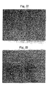
- a hydrogen ion implantation was carried out on this distorted SiGe/Si substrate (normalized elastic strain energy: 0.097) within the range of the "optimal condition" in the Rp-U SiGe graph and the distorted SiGe/Si substrate was annealed at 800°C for 10 minutes in an Ar atmosphere. No surface roughness was observed and the surface was smooth as shown in Fig. 22 when the surface of the SiGe film of which the distortion had been relaxed as described above was observed using a Nomarski microscope.
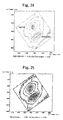
- the relaxation ratio of the SiGe film was 81.2 % indicating a sufficient relaxation of the distortion and that the crystallinity was excellent as shown in Fig. 24 according to XRD analysis of the (-2-2 4) surface of this SiGe film.
- a distorted SiGe/Si substrate was formed by epitaxially growing the first SiGe film in a virtual lattice form at 500°C so as to have a Ge concentration of 24.1 % and so as to have a film thickness of 304 nm in the same manner as described above. Hydrogen ions were implanted into this distorted SiGe/Si substrate (normalized elastic strain energy: 0.177) within the range of optimal condition and the distorted SiGe/Si substrate was annealed at 800°C for 10 minutes in an H 2 atmosphere. No surface roughness was observed as shown in Fig. 23 and the surface was very smooth when the surface of the SiGe film of which the distortion had been relaxed as described above was observed using a Nomarski microscope.
- Figs. 6 (a) to (d) are diagrams showing the steps of a method for improving the quality of a semiconductor substrate according to Embodiment 4 of the present invention. Here the effects in the case wherein another semiconductor film is formed on the SiGe film were examined.
- a distorted SiGe/Si substrate was formed by epitaxially growing the first SiGe film in a virtual lattice form at 500°C so as to have a Ge concentration of 28.8% and so as to have a film thickness of 158 nm (Fig. 6(a)).
- Ion implantation of hydrogen ions 3 was carried out on this distorted SiGe/ Si substrate under the conditions wherein the implementation energy was 18 KeV, the amount of implanted hydrogen ions (dose) was 3 ⁇ 10 16 H + /cm 2 and the angle of tilt was 7° (Fig. 6(b)).
- the peak depth Rp of the hydrogen ions in this ion implantation condition is located at a position in the Si substrate 72 nm away from the SiGe/Si interface.
- the substrate in which the hydrogen ions had been implemented was annealed at 800°C for 10 minutes using a furnace in an N 2 atmosphere (Fig. 6(c)).
- the value of (Rp, U SiGe ) is in the range of the "optimal condition" of Fig. 1. It was found according to XRD analysis of the (-2-2 4) surface of the SiGe film of which the distortion had been relaxed, in accordance with the above described conditions, that the relaxation ratio of the SiGe film was 80.1 % indicating a sufficient relaxation, as shown in Fig. 17, and the crystallinity was excellent.
- the second SiGe film in a virtual lattice form was epitaxially grown at 500°C so as to have a Ge concentration of 30% and so as to have a film thickness of 300 nm on the SiGe film, wherein the distortion had been relaxed (Fig. 6(d)). Thereby, the total film thickness of the first and second SiGe films became 458 nm.
- the second SiGe film was layered on top of the SiGe film, wherein the distortion had been relaxed as described above and thereby, by means of a CMOS device having a high source voltage for example, the diffusion of the depletion layer region was able to reach to the interface between the first SiGe film and the Si substrate wherein misfit dislocations exist and, thereby, junction leak current was able to be prevented.
- Figs. 7 (a) to (d) are diagrams showing the steps of a method for improving the quality of a semiconductor substrate according to Embodiment 5 of the present invention.
- the effects in the case wherein a Si film was formed on a SiGe film were examined.
- a distorted SiGe/ Si substrate was formed by epitaxially growing the first SiGe film in a virtual lattice form at 500°C so as to have a Ge concentration of 28.8% and so as to have a film thickness of 158 nm (Fig. 7(a)).
- Ion implantation of hydrogen ions 3 was carried out on this distorted SiGe/Si substrate under the conditions wherein the implementation energy was 18 KeV, the amount of implanted hydrogen ions (dose) was 3 ⁇ 10 16 H + /cm 2 and the angle of tilt was 7° (Fig. 7(b)).
- the peak depth Rp of the hydrogen ions in this ion implantation condition is located at a position in the Si substrate 72 nm away from the SiGe/Si interface.
- the substrate in which the hydrogen ions had been implemented was annealed at 800°C for 10 minutes using a furnace in an N 2 atmosphere (Fig. 7(c)).
- the value of (Rp, U SiGe ) is in the range of the "optimal condition" of Fig. 1. It was found according to XRD analysis of the (-2-2 4) surface of the SiGe film of which the distortion had been relaxed, in accordance with the above described conditions, that the relaxation ratio of the SiGe film was 80.1% indicating a sufficient relaxation and the crystallinity was excellent, as shown in Fig. 17.
- the second SiGe film in a virtual lattice form was epitaxially grown at 500°C so as to have a Ge concentration of 30% and so as to have a film thickness of 300 nm on the SiGe film, of which the distortion had been relaxed, and, after that, another Si film in a virtual lattice form was grown so as to have a film thickness of 20 nm (Fig. 7(d)).
- This Si thin film formed on the second SiGe film was formed in a virtual lattice form and, therefore, the lattice was stretched by the second SiGe film, of which the distortion had been relaxed, having a lattice constant greater than that of the Si film so that the mobility of electrons and holes in the Si thin film was increased.
- a MOS device was formed in a Si thin film that was similar to that of Embodiment 5 so as to inspect the functioning of the device.
- the first SiGe film was epitaxially grown at 500°C so as to be in a virtual lattice form, so as to have a Ge concentration of 28.8% and so as to have a film thickness of 158 nm and a distorted SiGe/Si substrate was formed wherein ion implantation of hydrogen ions was carried out on this distorted SiGe/Si substrate under conditions wherein the implantation energy was 18 KeV, the amount of implanted hydrogen ions (dose) was 3 ⁇ 10 16 H + /cm 2 and the angle of tilt was 7°.
- the peak depth Rp of the hydrogen ions under these ion implantation condition is located at a position in the Si substrate 72 nm away from the SiGe/Si interface.
- the substrate into which the hydrogen ions had been implanted was annealed at 800°C for 10 minutes using a furnace in an N 2 atmosphere.
- the value of (Rp, U SiGe ) is within the range of the "optimal condition" of Fig. 1.
- the second SiGe film was formed so as to have a Ge concentration of 30% and so as to have a film thickness of 300 nm and Si was grown on top of that so as to be in a virtual lattice form and so as to have a film thickness of 20 nm and, thereby, a distorted Si/SiGe/Si substrate was formed.
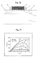
- a PMOS having the structure shown in Fig. 26 was formed on the distorted Si/SiGe/Si substrate.
- a Si substrate denoted as 1, a SiGe film denoted as 2, and a Si film denoted as 8 in the figure were formed according to the above described procedure.
- a gate oxide film 11 and a gate electrode 10 were formed by patterning this substrate and ion implantation of boron was carried out using the gate oxide film 11 and the gate electrode 10 as a mask in a self-aligning manner and, after that, thermal diffusion was carried out and, thereby, a source 13 and a drain 14 were formed and, in addition, sidewalls 12 were formed so that the PMOS was formed.
- the distorted Si/SiGe/Si substrate had an upper layer Si thin film grown on the SiGe film, of which the distortion had been relaxed according to the "optimal conditions," and, therefore, a stretch distortion occured in the upper layer Si thin film.
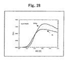
- the distorted Si/SiGe interface was smooth and flat. Therefore, as shown in Fig. 27, the Id-Vd characteristics exhibited an increased drain current in comparison with that of a PMOS in a conventional Si substrate and, as shown in Fig. 28, the Gm-Vg characteristics exhibited a greater maximum value of Gm than that of a PMOS in a conventional Si substrate. Therefore, an increase in carrier mobility (here holes) was able to be confirmed.
- a predetermined range of appropriate conditions for quality improvement can be expressed using three parameters: elastic strain energy U SiGe ; the peak depth Rp; and amount of implanted ions and, therefore, the optimal hydrogen ion implantation condition, which depends on conditions such as the Ge concentration and the thickness of the SiGe film, can be determined using these parameters so that distortion relaxed SiGe film having an excellent surface condition, excellent crystallinity and a sufficient relaxation ratio can be formed.
- a Si substrate wherein carrier mobility is greater than that of a conventional Si substrate can be provided by forming a Si thin film on a distortion relaxed SiGe film and it becomes possible to manufacture an excellent semiconductor device.
Landscapes
- Recrystallisation Techniques (AREA)
- Insulated Gate Type Field-Effect Transistor (AREA)
- Thin Film Transistor (AREA)
Abstract
and
Description


wherein the normalized energy was greater than 0.266.
wherein the amount of implanted ions was 3 × 10¹⁶ H+/cm2.
wherein the implantation energy was 33 KeV, the amount of implanted hydrogen ions (dose) was 4 × 10¹⁶ H+/cm2 and the angle of tilt was 7°.
wherein another semiconductor film is formed on the SiGe film were examined.
wherein the distortion had been relaxed as described above and thereby, by means of a CMOS device having a high source voltage for example, the diffusion of the depletion layer region was able to reach to the interface between the first SiGe film and the Si substrate wherein misfit dislocations exist and, thereby, junction leak current was able to be prevented.
wherein a Si film was formed on a SiGe film were examined.
Claims (10)
- A method for improving a semiconductor substrate having a SiGe film on a Si or SOI substrate by using a hydrogen ion implantation and an annealing, wherein the hydrogen ion implantation comprises the steps of:determining in advance the range of an improvement conditions by three parameters consisting of the following (1), (2) and (3),(1) an elastic strain energy USiGe which depends on a Ge concentration of the SiGe film and on a thickness of the SiGe film,(2) a peak depth Rp which is a distance between a SiGe/Si interface and a peak position of hydrogen ion concentration in the Si or SOI substrate and which depends on hydrogen ion implantation energy and on the thickness of the SiGe film, and(3) an amount of hydrogen ions to be implanted;selecting a desired improvement condition from the range of the improvement conditions;anddetermining an amount of hydrogen ions to be implanted and a hydrogen ion implantation energy.
- The method of claim 1, wherein the elastic strain energy USiGe and the the peak depth Rp are selected as the parameters and the amount of hydrogen ions is selected as a sub parameter, and the hydrogen ion implantation further comprises the steps of:calculating the elastic strain energy USiGe from both the Ge concentration and the thickness of the SiGe film;provisionally setting the amount of hydrogen ions to be implanted and the hydrogen ion implantation energy;calculating the peak depth Rp from both the thickness of the SiGe film and the provisionally set hydrogen ion implantation energy;determining whether or not the calculated elastic strain energy USiGe, the calculated peak depth Rp and the provisionally set amount of hydrogen ions to be implanted are in a range of the improvement conditions predetermined with respect to each previously set amount of hydrogen ions to be implanted; anddetermining the hydrogen implantation energy and the amount of hydrogen ions to be implanted as the ion implantation conditions, respectively, if the calculated hydrogen ion implantation energy, the calculated the peak depth Rp and the provisionally set amount of hydrogen ions to be implanted are in the range of the improvement conditions.
- The method of claim 1, wherein the elastic strain energy USiGe is not greater than a normalized value of 0.266.
- The method of claim 1, wherein the amount of hydrogen ions to be implanted is in the range of 2 × 10¹⁶ to 4 × 10¹⁶ H+ / cm2.
- The method of claim 2, wherein the range of the improvement conditions is determined by the parameter of the elastic strain energy USiGe and the parameter of the peak depth parameter Rp when the previously set amount of hydrogen ions to be implanted is 2 × 10¹⁶, 3 × 10¹⁶, or 4 × 10¹⁶ H+/ cm2.
- The method of claim 1, wherein a Si oxide film, a Si nitride film or a Si oxide nitride film is formed as a protection film on the SiGe film.
- The method of claim 1, wherein the annealing process is carried out in a nitrogen, argon, or hydrogen atmosphere.
- A semiconductor device, comprising:a semiconductor substrate having a SiGe film improved by the method of claim 1, andan upper layer semiconductor film including at least one layer, the upper layer semiconductor film being formed on the SiGe film of the semiconductor substrate.
- The device of claim 8, further comprising a top layer semiconductor film formed of a Si film.
- The device of claim 9, further comprising a MOS transistor having a gate oxide film and a gate electrode formed on the top layer semiconductor film and having a source and a drain formed at positions lower than the Si film.
Applications Claiming Priority (2)
| Application Number | Priority Date | Filing Date | Title |
|---|---|---|---|
| JP2002241010 | 2002-08-21 | ||
| JP2002241010A JP2004079912A (en) | 2002-08-21 | 2002-08-21 | Semiconductor substrate reforming method and semiconductor device using this method |
Publications (2)
| Publication Number | Publication Date |
|---|---|
| EP1391937A2 true EP1391937A2 (en) | 2004-02-25 |
| EP1391937A3 EP1391937A3 (en) | 2006-06-14 |
Family
ID=31185201
Family Applications (1)
| Application Number | Title | Priority Date | Filing Date |
|---|---|---|---|
| EP03018848A Withdrawn EP1391937A3 (en) | 2002-08-21 | 2003-08-19 | Method for improving a semiconductor substrate having SiGe film and semiconductor device manufactured by using this method |
Country Status (5)
| Country | Link |
|---|---|
| US (1) | US7348186B2 (en) |
| EP (1) | EP1391937A3 (en) |
| JP (1) | JP2004079912A (en) |
| KR (1) | KR100519202B1 (en) |
| TW (1) | TWI248118B (en) |
Cited By (1)
| Publication number | Priority date | Publication date | Assignee | Title |
|---|---|---|---|---|
| CN113109415A (en) * | 2021-03-26 | 2021-07-13 | 南昌大学 | Multilayer film interface position characterization method suitable for secondary ion mass spectrometry |
Families Citing this family (17)
| Publication number | Priority date | Publication date | Assignee | Title |
|---|---|---|---|---|
| US6855649B2 (en) * | 2001-06-12 | 2005-02-15 | International Business Machines Corporation | Relaxed SiGe layers on Si or silicon-on-insulator substrates by ion implantation and thermal annealing |
| DE10310740A1 (en) * | 2003-03-10 | 2004-09-30 | Forschungszentrum Jülich GmbH | Method for producing a stress-relaxed layer structure on a non-lattice-matched substrate, and use of such a layer system in electronic and / or optoelectronic components |
| US7273818B2 (en) * | 2003-10-20 | 2007-09-25 | Tokyo Electron Limited | Film formation method and apparatus for semiconductor process |
| DE102004031710B4 (en) * | 2004-06-30 | 2007-12-27 | Advanced Micro Devices, Inc., Sunnyvale | Method for producing differently deformed semiconductor regions and transistor pair in differently shaped semiconductor regions |
| DE102004048096A1 (en) * | 2004-09-30 | 2006-04-27 | Forschungszentrum Jülich GmbH | Method for producing a strained layer on a substrate and layer structure |
| US7273800B2 (en) * | 2004-11-01 | 2007-09-25 | International Business Machines Corporation | Hetero-integrated strained silicon n- and p-MOSFETs |
| JP5141029B2 (en) * | 2007-02-07 | 2013-02-13 | 富士通セミコンダクター株式会社 | Semiconductor device and manufacturing method thereof |
| JP5465830B2 (en) * | 2007-11-27 | 2014-04-09 | 信越化学工業株式会社 | Manufacturing method of bonded substrate |
| KR100908653B1 (en) | 2007-12-21 | 2009-07-21 | 한국지질자원연구원 | Depth Uniform Distribution of Atoms by Inclined Ion Implantation |
| KR101259000B1 (en) * | 2011-07-08 | 2013-04-29 | 단국대학교 산학협력단 | method of changing property of thin film |
| US8859348B2 (en) | 2012-07-09 | 2014-10-14 | International Business Machines Corporation | Strained silicon and strained silicon germanium on insulator |
| JP6539959B2 (en) * | 2014-08-28 | 2019-07-10 | 株式会社Sumco | Epitaxial silicon wafer, method of manufacturing the same, and method of manufacturing solid-state imaging device |
| US10833175B2 (en) * | 2015-06-04 | 2020-11-10 | International Business Machines Corporation | Formation of dislocation-free SiGe finFET using porous silicon |
| US9570298B1 (en) | 2015-12-09 | 2017-02-14 | International Business Machines Corporation | Localized elastic strain relaxed buffer |
| JP6787268B2 (en) * | 2017-07-20 | 2020-11-18 | 株式会社Sumco | Semiconductor epitaxial wafer and its manufacturing method, and solid-state image sensor manufacturing method |
| JP7195241B2 (en) * | 2019-01-09 | 2022-12-23 | 東京エレクトロン株式会社 | Nitride Film Forming Method and Nitride Film Forming Apparatus |
| CN119804060A (en) * | 2024-12-27 | 2025-04-11 | 四川大学 | Preparation technology of standard sample for hydrogen isotope homogenization based on energy regulator ion implantation |
Family Cites Families (5)
| Publication number | Priority date | Publication date | Assignee | Title |
|---|---|---|---|---|
| US5706164A (en) * | 1996-07-17 | 1998-01-06 | Vangaurd International Semiconductor Corporation | Method of fabricating high density integrated circuits, containing stacked capacitor DRAM devices, using elevated trench isolation and isolation spacers |
| US6593625B2 (en) * | 2001-06-12 | 2003-07-15 | International Business Machines Corporation | Relaxed SiGe layers on Si or silicon-on-insulator substrates by ion implantation and thermal annealing |
| US6583000B1 (en) * | 2002-02-07 | 2003-06-24 | Sharp Laboratories Of America, Inc. | Process integration of Si1-xGex CMOS with Si1-xGex relaxation after STI formation |
| US6562703B1 (en) * | 2002-03-13 | 2003-05-13 | Sharp Laboratories Of America, Inc. | Molecular hydrogen implantation method for forming a relaxed silicon germanium layer with high germanium content |
| US6841457B2 (en) * | 2002-07-16 | 2005-01-11 | International Business Machines Corporation | Use of hydrogen implantation to improve material properties of silicon-germanium-on-insulator material made by thermal diffusion |
-
2002
- 2002-08-21 JP JP2002241010A patent/JP2004079912A/en active Pending
-
2003
- 2003-08-13 US US10/639,647 patent/US7348186B2/en not_active Expired - Fee Related
- 2003-08-15 TW TW092122556A patent/TWI248118B/en not_active IP Right Cessation
- 2003-08-19 EP EP03018848A patent/EP1391937A3/en not_active Withdrawn
- 2003-08-20 KR KR10-2003-0057651A patent/KR100519202B1/en not_active Expired - Fee Related
Non-Patent Citations (6)
| Title |
|---|
| FOLLSTAEDT D M ET AL: "Cavty-dislocation interactions in Si-Ge and implications for heterostructure relaxation" APPLIED PHYSICS LETTERS, AIP, AMERICAN INSTITUTE OF PHYSICS, MELVILLE, NY, US, vol. 69, no. 14, 18 July 1996 (1996-07-18), pages 2059-2061, XP002250275 ISSN: 0003-6951 * |
| HOLLANDER B ET AL: "Strain relaxation of pseudomorphic Si1-xGex/Si(100) heterostructures after hydrogen or helium ion implantation for virtual substrate fabrication" NUCLEAR INSTRUMENTS & METHODS IN PHYSICS RESEARCH, SECTION - B: BEAM INTERACTIONS WITH MATERIALS AND ATOMS, ELSEVIER, AMSTERDAM, NL, vol. 175-177, April 2001 (2001-04), pages 357-367, XP004242660 ISSN: 0168-583X * |
| MANTL S ET AL: "Strain relaxation of epitaxial SiGe layers on Si(100) improved by hydrogen implantation" NUCLEAR INSTRUMENTS & METHODS IN PHYSICS RESEARCH, SECTION - B: BEAM INTERACTIONS WITH MATERIALS AND ATOMS, ELSEVIER, AMSTERDAM, NL, vol. 147, no. 1-4, January 1999 (1999-01), pages 29-34, XP004196272 ISSN: 0168-583X * |
| MII Y J ET AL: "EXTREMELY HIGH ELECTRON MOBILITY IN SI/GEXSI1-X STRUCTURES GROWN BY MOLECULAR BEAM EPITAXY" APPLIED PHYSICS LETTERS, AIP, AMERICAN INSTITUTE OF PHYSICS, MELVILLE, NY, US, vol. 59, no. 13, 23 September 1991 (1991-09-23), pages 1611-1613, XP000235506 ISSN: 0003-6951 * |
| MUHLBERGER M ET AL: "High-speed transport in Si/Si1-x-yGexCy heterostructures" THIN SOLID FILMS, ELSEVIER-SEQUOIA S.A. LAUSANNE, CH, vol. 369, no. 1-2, July 2000 (2000-07), pages 306-311, XP004200378 ISSN: 0040-6090 * |
| TRINKAUS H ET AL: "Strain relaxation mechanism for hydrogen-implanted Si1-xGex/Si(100) heterostructures" APPLIED PHYSICS LETTERS, AIP, AMERICAN INSTITUTE OF PHYSICS, MELVILLE, NY, US, vol. 76, no. 24, 12 June 2000 (2000-06-12), pages 3552-3554, XP012025523 ISSN: 0003-6951 * |
Cited By (1)
| Publication number | Priority date | Publication date | Assignee | Title |
|---|---|---|---|---|
| CN113109415A (en) * | 2021-03-26 | 2021-07-13 | 南昌大学 | Multilayer film interface position characterization method suitable for secondary ion mass spectrometry |
Also Published As
| Publication number | Publication date |
|---|---|
| TWI248118B (en) | 2006-01-21 |
| US7348186B2 (en) | 2008-03-25 |
| JP2004079912A (en) | 2004-03-11 |
| TW200407977A (en) | 2004-05-16 |
| KR100519202B1 (en) | 2005-10-06 |
| KR20040018166A (en) | 2004-03-02 |
| EP1391937A3 (en) | 2006-06-14 |
| US20040058482A1 (en) | 2004-03-25 |
Similar Documents
| Publication | Publication Date | Title |
|---|---|---|
| US7348186B2 (en) | Method for improving a semiconductor substrate having SiGe film and semiconductor device manufactured by using this method | |
| US6982208B2 (en) | Method for producing high throughput strained-Si channel MOSFETS | |
| US9309607B2 (en) | Semiconductor heterostructures having reduced dislocation pile-ups and related methods | |
| US6043139A (en) | Process for controlling dopant diffusion in a semiconductor layer | |
| US6946373B2 (en) | Relaxed, low-defect SGOI for strained Si CMOS applications | |
| US6709903B2 (en) | Relaxed SiGe layers on Si or silicon-on-insulator substrates by ion implantation and thermal annealing | |
| US20120244688A1 (en) | Selective epitaxial formation of semiconductive films | |
| JP2004014856A (en) | Method for manufacturing semiconductor substrate and method for manufacturing semiconductor device | |
| JP2003273017A (en) | Method of manufacturing relaxed SiGe substrate | |
| JP2007511892A (en) | Epitaxial growth of relaxed silicon germanium layers. | |
| US7198997B2 (en) | Method for producing semiconductor substrate, method for producing field effect transistor, semiconductor substrate, and field effect transistor | |
| US6869897B2 (en) | Manufacturing method for semiconductor substrate, and semiconductor device having a strained Si layer | |
| US7030002B2 (en) | Low temperature anneal to reduce defects in hydrogen-implanted, relaxed SiGe layer | |
| Dobbie et al. | Growth of smooth, low-defect germanium layers on (111) silicon via an intermediate islanding process | |
| US7202142B2 (en) | Method for producing low defect density strained -Si channel MOSFETS | |
| Ye et al. | A study of low energy phosphorus implantation and annealing in Si: C epitaxial films | |
| KR100632460B1 (en) | Manufacturing Method of Semiconductor Device | |
| WO2002001624A1 (en) | Semiconductor component and method of manufacturing | |
| JP2003282471A (en) | Semiconductor substrate manufacturing method |
Legal Events
| Date | Code | Title | Description |
|---|---|---|---|
| PUAI | Public reference made under article 153(3) epc to a published international application that has entered the european phase |
Free format text: ORIGINAL CODE: 0009012 |
|
| AK | Designated contracting states |
Kind code of ref document: A2 Designated state(s): AT BE BG CH CY CZ DE DK EE ES FI FR GB GR HU IE IT LI LU MC NL PT RO SE SI SK TR |
|
| AX | Request for extension of the european patent |
Extension state: AL LT LV MK |
|
| PUAL | Search report despatched |
Free format text: ORIGINAL CODE: 0009013 |
|
| AK | Designated contracting states |
Kind code of ref document: A3 Designated state(s): AT BE BG CH CY CZ DE DK EE ES FI FR GB GR HU IE IT LI LU MC NL PT RO SE SI SK TR |
|
| AX | Request for extension of the european patent |
Extension state: AL LT LV MK |
|
| 17P | Request for examination filed |
Effective date: 20061018 |
|
| AKX | Designation fees paid |
Designated state(s): DE FR |
|
| 17Q | First examination report despatched |
Effective date: 20090205 |
|
| STAA | Information on the status of an ep patent application or granted ep patent |
Free format text: STATUS: THE APPLICATION IS DEEMED TO BE WITHDRAWN |
|
| 18D | Application deemed to be withdrawn |
Effective date: 20090616 |