EP1391894B1 - Magnetic memory array and its read/write method - Google Patents
Magnetic memory array and its read/write method Download PDFInfo
- Publication number
- EP1391894B1 EP1391894B1 EP03018621A EP03018621A EP1391894B1 EP 1391894 B1 EP1391894 B1 EP 1391894B1 EP 03018621 A EP03018621 A EP 03018621A EP 03018621 A EP03018621 A EP 03018621A EP 1391894 B1 EP1391894 B1 EP 1391894B1
- Authority
- EP
- European Patent Office
- Prior art keywords
- magnetic layer
- magnetic
- handed
- magnetic memory
- magnetization
- Prior art date
- Legal status (The legal status is an assumption and is not a legal conclusion. Google has not performed a legal analysis and makes no representation as to the accuracy of the status listed.)
- Expired - Lifetime
Links
- 230000005291 magnetic effect Effects 0.000 title claims description 206
- 230000015654 memory Effects 0.000 title claims description 76
- 238000000034 method Methods 0.000 title claims description 27
- 230000005415 magnetization Effects 0.000 claims description 56
- 239000003302 ferromagnetic material Substances 0.000 claims description 9
- 230000005290 antiferromagnetic effect Effects 0.000 claims description 8
- 230000008859 change Effects 0.000 claims description 6
- 230000008569 process Effects 0.000 description 8
- 230000004907 flux Effects 0.000 description 6
- 230000007704 transition Effects 0.000 description 6
- 230000003247 decreasing effect Effects 0.000 description 4
- 239000000696 magnetic material Substances 0.000 description 3
- 229910003271 Ni-Fe Inorganic materials 0.000 description 2
- 230000003993 interaction Effects 0.000 description 2
- 229910020598 Co Fe Inorganic materials 0.000 description 1
- 229910002519 Co-Fe Inorganic materials 0.000 description 1
- 229910017061 Fe Co Inorganic materials 0.000 description 1
- 229910002551 Fe-Mn Inorganic materials 0.000 description 1
- 229910000914 Mn alloy Inorganic materials 0.000 description 1
- 229910045601 alloy Inorganic materials 0.000 description 1
- 239000000956 alloy Substances 0.000 description 1
- 239000002885 antiferromagnetic material Substances 0.000 description 1
- 229910052802 copper Inorganic materials 0.000 description 1
- 238000011161 development Methods 0.000 description 1
- 230000018109 developmental process Effects 0.000 description 1
- 230000000694 effects Effects 0.000 description 1
- 230000005294 ferromagnetic effect Effects 0.000 description 1
- 230000006870 function Effects 0.000 description 1
- 229910052737 gold Inorganic materials 0.000 description 1
- 229910052741 iridium Inorganic materials 0.000 description 1
- 230000004048 modification Effects 0.000 description 1
- 238000012986 modification Methods 0.000 description 1
- 229910052697 platinum Inorganic materials 0.000 description 1
- 230000002285 radioactive effect Effects 0.000 description 1
- 238000011160 research Methods 0.000 description 1
- 238000012552 review Methods 0.000 description 1
- 229910052709 silver Inorganic materials 0.000 description 1
Images



Classifications
-
- G—PHYSICS
- G11—INFORMATION STORAGE
- G11C—STATIC STORES
- G11C11/00—Digital stores characterised by the use of particular electric or magnetic storage elements; Storage elements therefor
- G11C11/02—Digital stores characterised by the use of particular electric or magnetic storage elements; Storage elements therefor using magnetic elements
- G11C11/14—Digital stores characterised by the use of particular electric or magnetic storage elements; Storage elements therefor using magnetic elements using thin-film elements
- G11C11/15—Digital stores characterised by the use of particular electric or magnetic storage elements; Storage elements therefor using magnetic elements using thin-film elements using multiple magnetic layers
-
- G—PHYSICS
- G11—INFORMATION STORAGE
- G11C—STATIC STORES
- G11C11/00—Digital stores characterised by the use of particular electric or magnetic storage elements; Storage elements therefor
- G11C11/02—Digital stores characterised by the use of particular electric or magnetic storage elements; Storage elements therefor using magnetic elements
- G11C11/16—Digital stores characterised by the use of particular electric or magnetic storage elements; Storage elements therefor using magnetic elements using elements in which the storage effect is based on magnetic spin effect
Definitions
- This invention relates to a nonvolatile magnetic memory and a magnetic memory array which are preferably usable as a magnetic random access memory (MRAM). Also, this invention relates to a method for recording in the nonvolatile magnetic memory and a method for reading out from the nonvolatile magnetic memory.
- MRAM magnetic random access memory
- such a magnetic memory cell is shaped rectangular, and information "0" or "1" is stored on the magnetic direction of the magnetic memory cell.
- the magnetic flux originated from the magnetization is leaked outside from the magnetic memory cell due to the configuration thereof.
- such an attempt is made as to arrange a plurality of magnetic memory cells in high density. In this case, however, the leaked magnetic flux affects significantly on the adjacent magnetic memory cells, and thus, the intended high density MRAM can not be realized.
- the vortex magnetization can not be created and thus, it may be that information recording utilizing the vortex magnetization can not be realized ([ Physical Review Letters, 83, No. 5, pp1042-1045 (1999 )].
- this invention relates to a magnetic memory comprising a ring-shaped magnetic layer having a notch formed by partially cutting out the periphery thereof in circular arc shape.
- the inventors found out through vast researches and developments that if the periphery of the ring-shaped magnetic layer constituting the magnetic memory is partially cut so that the resultant cross sectional surface is perpendicular to the radial direction of the magnetic memory, the clockwise magnetization and the anticlockwise magnetization can be easily created in vortex even though the thickness of the magnetic layer is small.
- the vortex magnetization can be easily created in the magnetic layer, and information "0" or "1” can be recorded in the magnetic layer on the rotative direction of the vortex magnetization.
- Fig. 1 is a structural view schematically showing a magnetic layer constituting a magnetic memory according to the present invention
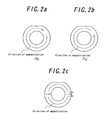
- Fig. 2 are views showing the states of magnetization in the magnetic layer shown in Fig. 1 .
- the magnetic layer 11 is shaped in ring, and the periphery of the magnetic layer 11 is partially cut out so that the resultant cross sectional surface is perpendicular to the radial direction of the magnetic layer 11.
- a circular arc notch is formed at the periphery of the magnetic layer 11.
- a vortex magnetization of right- handed (clockwise) direction or left-handed (anticlockwise) direction can be created in the magnetic layer 12 as shown in Figs. 2(a) and 2(b) .
- the right-handed (clockwise) magnetization and the (left-handed (anticlockwise) magnetization are created in the magnetic layer 11 by the application of magnetic field with a strength within 500-2000Oe.
- a state of magnetization as shown in Fig. 2(c) appears in the transition of the state of magnetization shown in Fig. 2(b) from the one shown in Fig. 2(a) or the transition of the state of magnetization shown in Fig. 2(a) from the one shown in Fig. 2(b) .
- the ratio (h/H1) is preferably set to 0.01 or over, particularly 0.05 over. Therefore, if the notch 12 is formed by cutting the periphery of the magnetic layer 11 so as to satisfy the above-mentioned relation, the object of the present invention can be realized more effectively.
- the upper limited value of the ratio (h/H1) is not restricted, it may be preferably set to 0.2. If the ratio (h/H1) is set over the upper limited value of 0.2, the effect/function of the present invention can not be enhanced, and it may be that a vortex magnetization can not be created in the magnetic layer 11 to be not able to be employed as a magnetic memory.
- the magnetic layer 11 may be made of a room temperature ferromagnetic material such as Ni-Fe, Ni-Fe-Co or Co-Fe, for example.
- the "room temperature ferromagnetic material” means a magnetic material showing ferromagnetic property at room temperature. Therefore, other magnetic materials may be employed, instead of the above-mentioned ferromagnetic material such as Ni-Fe or the like.
- the thickness of the magnetic layer 11 is preferably set within 1-10nm particularly within 3-5nm. In this case, a sufficiently large vortex magnetization can be created in the magnetic layer 11, and thus, information can be stably stored when information "0" or "1" is allotted to the rotative direction of the vortex magnetization.
- Fig. 3 is a structural view showing a concrete magnetic memory according to the present invention.
- a magnetic layer 21 shown in Fig. 1 on a magnetic layer 21 shown in Fig. 1 are successively formed an additional magnetic layer 23 and an antiferromagnetic layer 24 via a non-magnetic layer 22.
- the magnetic layer 21 is shaped in ring, and the periphery of the magnetic layer 21 is partially cut out so as to form a notch thereat.
- the non-magnetic layer 22 through the antiferromagnetic layer 24 are shaped in ring concentrically for the magnetic layer 21.
- the magnetic layer 21 is magnetized in right-handed (clockwise) direction or left-handed (anticlockwise) direction, and information "0" or "1" is allotted to the rotative direction of the resultant vortex magnetization. In this way, recording process for the magnetic layer 21 is performed.
- the additional magnetic layer 23 is magnetized in right-handed (clockwise) direction or left-handed (anticlockwise) direction in advance, and the resultant vortex magnetization of the additional magnetic layer 23 is pinned through the bonding with exchanging interaction to the antiferromagnetic layer 24.
- the magnetic layer 21 and the additional magnetic layer 23 are magnetically divided by the non-magnetic layer 22.
- the magnetic layer 21 may be made of a room temperature ferromagnetic material as mentioned above, and the thickness of the magnetic layer 21 may be set within 1-10nm.
- the additional magnetic layer 23 may be made of such a room temperature ferromagnetic material as mentioned above, and the thickness of the additional magnetic layer 23 may be set within 1-10nm.
- the non-magnetic layer 22 may be made of a non-magnetic material such as Cu, Ag or Au, and the antiferromagnetic layer 24 may be made of an antiferromagnetic material such as Mn-Ir, Mn-Pt or Fe-Mn.
- the thickness of the non-magnetic layer 22 is set so as to magnetically divide the magnetic layer 21 and the additional magnetic layer 23.
- the thickness of the antiferromagnetic layer 24 is set so as to magnetically pin the magnetization of the additional magnetic layer 23 through the bonding with exchanging interaction.
- Fig. 4 are graphs conceptually showing the changes in electric resistance of the magnetic memory in switching process of magnetization.
- the electric resistance of the magnetic memory 30 is increased in the vicinity of zero-magnetic field as shown in Fig. 4(a) due to the transition of the state of magnetization (left-handed direction) shown in Fig. 2(b) from the one (right-handed direction) shown in Fig. 2(a)
- the electric resistance of the magnetic memory 30 is decreased in the vicinity of zero-magnetic field as shown in Fig. 4(b) due to the transition of the state of magnetization (left-handed direction) shown in Fig. 2(a) from the one (right-handed direction) shown in Fig. 2(b) .
- Reading process of recorded information ("0" and "1") from the magnetic memory 30 is carried out on the change in current of the magnetic memory 30 due to the change in resistance thereof depending on the relative position in magnetization between the magnetic layer 21 and the additional magnetic layer 23. That is, when the direction of the magnetization of the magnetic layer 21 is almost equal (parallel) to the direction of the magnetization of the additional magnetic layer 23, the electric resistance of the magnetic memory 30 is decreased. In this case, therefore, the current through the magnetic memory 30 is increased.
- the additional magnetic layer 23 is magnetized in right-handed (clockwise) direction or left-handed (anticlockwise) direction in advance, the electric resistance of the magnetic memory 30 is changed on the direction of the magnetization of the magnetic layer 21 through the application of magnetic field relating to recorded information "0" or "1". In this way, if the change in current of the magnetic memory 30 is measured, the recorded information ("0" and "1") can be read out of the magnetic memory 30 (magnetic layer 21).
- Each layer was shaped in ring, and the outer diameter and the inner diameter of each layer, that is, the magnetic memory were set to 1000nm and 500nm, respectively.
- the height of the resultant notch of the magnetic layer was set to 50nm.
- a given magnetic field was applied to the magnetic memory, and the change in magnetization of the magnetic layer functioning as a recording layer was simulated, and graphed in Fig. 5 .
- the fraction of the left-handed (anticlockwise) magnetization is increased in comparison with the fraction of the right-handed (clockwise) magnetization as shown in Figs. 5(a)-(e) while the strength of the applied magnetic field is varied from 2000Oe to -100Oe. In this case, therefore, the direction of the magnetization of the magnetic layer is changed from the right-handed direction to the left-handed direction.
- the fraction of the right-handed (clockwise) magnetization is increased in comparison with the fraction of the left-handed (anticlockwise) magnetization as shown in Figs. 5(f)-(j) while the strength of the applied magnetic field is varied from 100Oe to -2000e. In this case, therefore, the direction of the magnetization of the magnetic layer is changed from the left-handed direction to the right-handed direction.
- a magnetic memory and a magnetic memory array which can create a vortex magnetization irrespective of the thickness of the magnetic layer thereof and can perform recording process stably on the direction of the vortex magnetization can be provided. Moreover, a recording method and a reading method for the magnetic memory can be provided.
Landscapes
- Engineering & Computer Science (AREA)
- Computer Hardware Design (AREA)
- Semiconductor Memories (AREA)
- Hall/Mr Elements (AREA)
- Mram Or Spin Memory Techniques (AREA)
- Magnetic Record Carriers (AREA)
Description
- This invention relates to a nonvolatile magnetic memory and a magnetic memory array which are preferably usable as a magnetic random access memory (MRAM). Also, this invention relates to a method for recording in the nonvolatile magnetic memory and a method for reading out from the nonvolatile magnetic memory.
- Various electronic devices have been employed under a specific condition such as an aero-space, and thus, it is desired to establish a recording device where once stored information can not be deleted by the irradiation of a radioactive ray. In this point of view, large radioactive-resistance and nonvolatile MRAMs having their respective simply structured magnetic memory cells are researched and developed.
- Conventionally, such a magnetic memory cell is shaped rectangular, and information "0" or "1" is stored on the magnetic direction of the magnetic memory cell. With the conventional magnetic memory cell, however, the magnetic flux originated from the magnetization is leaked outside from the magnetic memory cell due to the configuration thereof. In order to increase the recording capacity of the MRAM, in contrast, such an attempt is made as to arrange a plurality of magnetic memory cells in high density. In this case, however, the leaked magnetic flux affects significantly on the adjacent magnetic memory cells, and thus, the intended high density MRAM can not be realized.
- In this point of view, the inventors have developed a ring-shaped magnetic memory where a right handed (clockwise) magnetization or a left-handed (anticlockwise) magnetization is created in vortex, and information "0" or "1" is stored on the rotative direction of the magnetization thereof (Japanese Patent application
2002-73681 - In this case, since a magnetic flux is not leaked from the magnetic memory, if a plurality of magnetic memory are arranged in high density as mentioned above, the leaked magnetic flux can not almost affect on the adjacent magnetic memories, so that a high density MRAM can be realized.
- As the thickness of the magnetic layer of the magnetic memory to store information is decreased, however, the vortex magnetization can not be created and thus, it may be that information recording utilizing the vortex magnetization can not be realized ([Physical Review Letters, 83, No. 5, pp1042-1045 (1999)].
- It is an object of the present invention to provide a magnetic memory and a magnetic memory array which can create a vortex magnetization, irrespective of the thickness of the magnetic layer constituting the magnetic memory and the magnetic memory array. It is another object of the present invention to provide a recording method and a reading method for the magnetic memory.
- In order to achieve the above-mentioned objects, this invention relates to a magnetic memory comprising a ring-shaped magnetic layer having a notch formed by partially cutting out the periphery thereof in circular arc shape.
- The inventors found out through vast researches and developments that if the periphery of the ring-shaped magnetic layer constituting the magnetic memory is partially cut so that the resultant cross sectional surface is perpendicular to the radial direction of the magnetic memory, the clockwise magnetization and the anticlockwise magnetization can be easily created in vortex even though the thickness of the magnetic layer is small.
- According to the present invention, therefore, even though the thickness of the magnetic layer is reduced within 1-10nm, the vortex magnetization can be easily created in the magnetic layer, and information "0" or "1" can be recorded in the magnetic layer on the rotative direction of the vortex magnetization.
- In the present invention, since a magnetic flux is not leaked from the magnetic layer due to the vortex magnetization, even though a plurality of magnetic memories having their respective magnetic layers are arranged in high density to form a magnetic memory array, no leaked magnetic flux affects on the adjacent magnetic memories. As a result, a practically usable high density magnetic memory array can be provided.
- Other features and advantages of the magnetic memory of the present invention will be described below. Also, a recording method and a reading method for the magnetic memory will be described below.
- For better understanding of the present invention, reference is made to the attached drawings, wherein
-
Fig. 1 is a structural view schematically showing a magnetic layer constituting a magnetic memory according to the present invention, -
Fig. 2 are views showing the states of magnetization in the magnetic layer shown inFig. 1 , -
Fig. 3 is a structural view showing a concrete magnetic memory according to the present invention, -
Fig. 4 are graphs conceptually showing the changes in electric resistance of the magnetic memory in switching process of magnetization, and -
Fig. 5 are simulated views showing the switching process of magnetization of the magnetic layer of the magnetic memory of the present invention. - This invention will be described in detail with reference to the accompanying drawings.
Fig. 1 is a structural view schematically showing a magnetic layer constituting a magnetic memory according to the present invention, andFig. 2 are views showing the states of magnetization in the magnetic layer shown inFig. 1 . As shown inFig. 1 , themagnetic layer 11 is shaped in ring, and the periphery of themagnetic layer 11 is partially cut out so that the resultant cross sectional surface is perpendicular to the radial direction of themagnetic layer 11. As a result, a circular arc notch is formed at the periphery of themagnetic layer 11. With the ring-shapedmagnetic layer 11 having thenotch 12, even though the thickness of themagnetic layer 11 is reduced within 1-10nm, for example, a vortex magnetization of right- handed (clockwise) direction or left-handed (anticlockwise) direction can be created in themagnetic layer 12 as shown inFigs. 2(a) and 2(b) . - As shown in
Fig. 2 , therefore, if the right-handed (clockwise) magnetization is allotted to information "0" and the left-handed (anticlockwise) magnetization is allotted to information "1", recording process can be performed for themagnetic layer 11. - The right-handed (clockwise) magnetization and the (left-handed (anticlockwise) magnetization are created in the
magnetic layer 11 by the application of magnetic field with a strength within 500-2000Oe. In the transition of the state of magnetization shown inFig. 2(b) from the one shown inFig. 2(a) or the transition of the state of magnetization shown inFig. 2(a) from the one shown inFig. 2(b) , such a state of magnetization as shown inFig. 2(c) appears. - If the height of the
notch 12 is defined as "h" and the outer diameter of the ring-shapedmagnetic layer 11 is defined as "H1", the ratio (h/H1) is preferably set to 0.01 or over, particularly 0.05 over. Therefore, if thenotch 12 is formed by cutting the periphery of themagnetic layer 11 so as to satisfy the above-mentioned relation, the object of the present invention can be realized more effectively. - Although the upper limited value of the ratio (h/H1) is not restricted, it may be preferably set to 0.2. If the ratio (h/H1) is set over the upper limited value of 0.2, the effect/function of the present invention can not be enhanced, and it may be that a vortex magnetization can not be created in the
magnetic layer 11 to be not able to be employed as a magnetic memory. - In order to maintain the ring shape of the
magnetic layer 11, it is required to satisfy the relation of "h<(H1-H2)/2 if the inner diameter of themagnetic layer 11 is defined as "H2". - The
magnetic layer 11 may be made of a room temperature ferromagnetic material such as Ni-Fe, Ni-Fe-Co or Co-Fe, for example. The "room temperature ferromagnetic material" means a magnetic material showing ferromagnetic property at room temperature. Therefore, other magnetic materials may be employed, instead of the above-mentioned ferromagnetic material such as Ni-Fe or the like. - The thickness of the
magnetic layer 11 is preferably set within 1-10nm particularly within 3-5nm. In this case, a sufficiently large vortex magnetization can be created in themagnetic layer 11, and thus, information can be stably stored when information "0" or "1" is allotted to the rotative direction of the vortex magnetization. -
Fig. 3 is a structural view showing a concrete magnetic memory according to the present invention. In themagnetic memory 30 shown inFig. 3 , on amagnetic layer 21 shown inFig. 1 are successively formed an additionalmagnetic layer 23 and anantiferromagnetic layer 24 via anon-magnetic layer 22. Themagnetic layer 21 is shaped in ring, and the periphery of themagnetic layer 21 is partially cut out so as to form a notch thereat. Thenon-magnetic layer 22 through theantiferromagnetic layer 24 are shaped in ring concentrically for themagnetic layer 21. - The
magnetic layer 21 is magnetized in right-handed (clockwise) direction or left-handed (anticlockwise) direction, and information "0" or "1" is allotted to the rotative direction of the resultant vortex magnetization. In this way, recording process for themagnetic layer 21 is performed. - In the
magnetic memory 30 shown inFig. 3 , the additionalmagnetic layer 23 is magnetized in right-handed (clockwise) direction or left-handed (anticlockwise) direction in advance, and the resultant vortex magnetization of the additionalmagnetic layer 23 is pinned through the bonding with exchanging interaction to theantiferromagnetic layer 24. Themagnetic layer 21 and the additionalmagnetic layer 23 are magnetically divided by thenon-magnetic layer 22. - The
magnetic layer 21 may be made of a room temperature ferromagnetic material as mentioned above, and the thickness of themagnetic layer 21 may be set within 1-10nm. The additionalmagnetic layer 23 may be made of such a room temperature ferromagnetic material as mentioned above, and the thickness of the additionalmagnetic layer 23 may be set within 1-10nm. - The
non-magnetic layer 22 may be made of a non-magnetic material such as Cu, Ag or Au, and theantiferromagnetic layer 24 may be made of an antiferromagnetic material such as Mn-Ir, Mn-Pt or Fe-Mn. The thickness of thenon-magnetic layer 22 is set so as to magnetically divide themagnetic layer 21 and the additionalmagnetic layer 23. The thickness of theantiferromagnetic layer 24 is set so as to magnetically pin the magnetization of the additionalmagnetic layer 23 through the bonding with exchanging interaction. - In the transition of the state of magnetization shown in
Fig. 2(b) from the one shown inFig. 2(a) or the transition of the state of magnetization shown inFig. 2(a) from the one shown inFig. 2(b) through the application of external magnetic field, the electric resistance of themagnetic memory 30 is varied remarkably on the direction of the magnetization of the additionalmagnetic layer 23. -
Fig. 4 are graphs conceptually showing the changes in electric resistance of the magnetic memory in switching process of magnetization. For example, if the additionalmagnetic layer 23 is magnetized in right-handed (clockwise) direction, in the switching process for themagnetic memory 30, the electric resistance of themagnetic memory 30 is increased in the vicinity of zero-magnetic field as shown inFig. 4(a) due to the transition of the state of magnetization (left-handed direction) shown inFig. 2(b) from the one (right-handed direction) shown inFig. 2(a) , and the electric resistance of themagnetic memory 30 is decreased in the vicinity of zero-magnetic field as shown inFig. 4(b) due to the transition of the state of magnetization (left-handed direction) shown inFig. 2(a) from the one (right-handed direction) shown inFig. 2(b) . - Reading process of recorded information ("0" and "1") from the
magnetic memory 30 is carried out on the change in current of themagnetic memory 30 due to the change in resistance thereof depending on the relative position in magnetization between themagnetic layer 21 and the additionalmagnetic layer 23. That is, when the direction of the magnetization of themagnetic layer 21 is almost equal (parallel) to the direction of the magnetization of the additionalmagnetic layer 23, the electric resistance of themagnetic memory 30 is decreased. In this case, therefore, the current through themagnetic memory 30 is increased. - In contrast, when the direction of the magnetization of the
magnetic layer 21 is almost opposite (anti-parallel) to the direction of the magnetization of the additionalmagnetic layer 23, the electric resistance of themagnetic memory 30 is increased. In this case, therefore, the current through themagnetic memory 30 is decreased. - In other words, the additional
magnetic layer 23 is magnetized in right-handed (clockwise) direction or left-handed (anticlockwise) direction in advance, the electric resistance of themagnetic memory 30 is changed on the direction of the magnetization of themagnetic layer 21 through the application of magnetic field relating to recorded information "0" or "1". In this way, if the change in current of themagnetic memory 30 is measured, the recorded information ("0" and "1") can be read out of the magnetic memory 30 (magnetic layer 21). - Example:
The magnetic layer and the additional magnetic layer were formed from Ni-20at% alloy in a thickness of 5nm, respectively, and the non-magnetic layer was formed from Cu in a thickness of 2.5nm, and the antiferromagnetic layer was formed from Fe-40at% Mn alloy to fabricate a magnetic memory as shown inFig. 3 . Each layer was shaped in ring, and the outer diameter and the inner diameter of each layer, that is, the magnetic memory were set to 1000nm and 500nm, respectively. The height of the resultant notch of the magnetic layer was set to 50nm. - A given magnetic field was applied to the magnetic memory, and the change in magnetization of the magnetic layer functioning as a recording layer was simulated, and graphed in
Fig. 5 . - As is apparent from
Fig. 5 , the fraction of the left-handed (anticlockwise) magnetization is increased in comparison with the fraction of the right-handed (clockwise) magnetization as shown inFigs. 5(a)-(e) while the strength of the applied magnetic field is varied from 2000Oe to -100Oe. In this case, therefore, the direction of the magnetization of the magnetic layer is changed from the right-handed direction to the left-handed direction. Similarly, the fraction of the right-handed (clockwise) magnetization is increased in comparison with the fraction of the left-handed (anticlockwise) magnetization as shown inFigs. 5(f)-(j) while the strength of the applied magnetic field is varied from 100Oe to -2000e. In this case, therefore, the direction of the magnetization of the magnetic layer is changed from the left-handed direction to the right-handed direction. - Although the present invention was described in detail with reference to the above examples, this invention is not limited to the above disclosure and every kind of variation and modification may be made without departing from the scope of the present invention.
- As mentioned above, according to the present invention, a magnetic memory and a magnetic memory array which can create a vortex magnetization irrespective of the thickness of the magnetic layer thereof and can perform recording process stably on the direction of the vortex magnetization can be provided. Moreover, a recording method and a reading method for the magnetic memory can be provided.
Claims (22)
- A magnetic memory comprising a ring-shaped magnetic layer (11) having a notch (12) formed by partially cutting out the periphery thereof in circular arc shape.
- The magnetic memory as defined in claim 1, wherein if the height of said notch formed at the periphery of said magnetic layer is defined as "h" and the outer diameter of said magnetic layer is defined as "H1", ratio (h/H1) is set to 0.01 or over.
- The magnetic memory as defined in claim 1 or 2, wherein said magnetic layer is made from room temperature ferromagnetic material.
- The magnetic memory as defined in any one of claims 1-3, wherein the thickness of said magnetic layer is set within 1-10nm.
- The magnetic memory as defined in any one of claims 1-4, wherein the direction of the magnetization of said magnetic layer is set to right-handed (clockwise) direction or left-handed (anticlockwise) direction in said magnetic layer.
- The magnetic memory as defined in any one of claims 1-5, further comprising a ring-shaped additional magnetic layer on said magnetic layer via a non-magnetic layer.
- The magnetic memory as defined in claim 6, wherein said additional magnetic layer is made from room temperature ferromagnetic material.
- The magnetic memory as defined in claim 6 or 7, wherein the thickness of said additional magnetic layer is set within 1-10nm.
- The magnetic memory as defined in any one of claims 6-8, further comprising an antiferromagnetic layer formed on a main surface of said additional magnetic layer opposite to said magnetic layer.
- The magnetic memory as defined in any one of claims 6-9, wherein the direction of the magnetization of said additional magnetic layer is set to right-handed (clockwise) direction or left-handed (anticlockwise) direction in said additional magnetic layer.
- The magnetic memory as defined in claim 9 or 10, wherein the direction of the magnetization of said additional magnetic layer is pinned.
- A magnetic memory array comprising a plurality of magnetic memories arranged regularly, each magnetic memory being defined in any one of claims 1-11.
- A method for recording in a magnetic memory with a ring-shaped magnetic layer, (11) comprising the steps of:partially cutting out the periphery of said magnetic layer in circular arc shape to form a notch (12) thereat, andmagnetizing said magnetic layer in right-handed (clockwise) direction or left-handed (anticlockwise) direction therein to record information "0" or "1" therein.
- The recording method as defined in claim 13, wherein if the height of said notch formed at the periphery of said magnetic layer is defined as "h" and the outer diameter of said magnetic layer is defined as "H1", ratio (h/H1) is set to 0.01 or over.
- The recording method as defined in claim 13 or 14, wherein said magnetic layer is made from room temperature ferromagnetic material.
- The recording method as defined in any one of claims 13-15, wherein the thickness of said magnetic layer is set within 1-10nm.
- A method for reading from a magnetic memory with a ring-shaped magnetic layer (11), comprising the steps of:partially cutting out the periphery of said magnetic layer in circular arc shape to form a notch (12) thereat,forming a ring-shaped additional magnetic layer on said magnetic layer via a non-magnetic layer,magnetizing in advance said additional magnetic layer in right-handed (clockwise) direction or left-handed (anticlockwise) direction therein,magnetizing said magnetic layer in right-handed (clockwise) direction or left-handed (anticlockwise) direction therein to record information "0" or "1" therein, andreading said information recorded in said magnetic layer on the change in current due to the change in electric resistance depending on the relative position in magnetization between said magnetic layer and said additional magnetic layer.
- The reading method as defined in claim 17, further comprising the step of forming an antiferromagnetic layer on a main surface of said additional magnetic layer opposite to said magnetic layer, thereby to pin the direction of the magnetization of said additional magnetic layer.
- The reading method as defined in claim 17 or 18, wherein if the height of said notch formed at the periphery of said magnetic layer is defined as "h" and the outer diameter of said magnetic layer is defined as "H1", ratio (h/H1) is set to 0.01 or over.
- The reading method as defined in any one of claims 17-19, wherein said magnetic layer is made from room temperature ferromagnetic material.
- The reading method as defined in any one of claims 17-20, wherein the thickness of said magnetic layer is set within 1-10nm.
- The reading method as defined in any one of claims 17-21, wherein the thickness of said additional magnetic layer is set within 1-10nm.
Applications Claiming Priority (2)
| Application Number | Priority Date | Filing Date | Title |
|---|---|---|---|
| JP2002242208 | 2002-08-22 | ||
| JP2002242208A JP4016101B2 (en) | 2002-08-22 | 2002-08-22 | Magnetic memory, magnetic memory array, magnetic memory recording method, and magnetic memory reading method |
Publications (3)
| Publication Number | Publication Date |
|---|---|
| EP1391894A2 EP1391894A2 (en) | 2004-02-25 |
| EP1391894A3 EP1391894A3 (en) | 2004-06-30 |
| EP1391894B1 true EP1391894B1 (en) | 2012-09-19 |
Family
ID=31185221
Family Applications (1)
| Application Number | Title | Priority Date | Filing Date |
|---|---|---|---|
| EP03018621A Expired - Lifetime EP1391894B1 (en) | 2002-08-22 | 2003-08-19 | Magnetic memory array and its read/write method |
Country Status (4)
| Country | Link |
|---|---|
| US (1) | US6950332B2 (en) |
| EP (1) | EP1391894B1 (en) |
| JP (1) | JP4016101B2 (en) |
| KR (1) | KR100563423B1 (en) |
Families Citing this family (10)
| Publication number | Priority date | Publication date | Assignee | Title |
|---|---|---|---|---|
| JP3987924B2 (en) * | 2002-12-13 | 2007-10-10 | 国立大学法人大阪大学 | Magnetic memory array, magnetic memory array writing method, and magnetic memory array reading method |
| US6952364B2 (en) | 2003-03-03 | 2005-10-04 | Samsung Electronics Co., Ltd. | Magnetic tunnel junction structures and methods of fabrication |
| JP3546238B1 (en) * | 2003-04-23 | 2004-07-21 | 学校法人慶應義塾 | Magnetic ring unit and magnetic memory device |
| KR100615089B1 (en) | 2004-07-14 | 2006-08-23 | 삼성전자주식회사 | Magnetic ram with low drive current |
| KR100568512B1 (en) | 2003-09-29 | 2006-04-07 | 삼성전자주식회사 | Magnetothermal Ramcells with a Heat Generating Layer and Methods of Driving Them |
| KR100835275B1 (en) | 2004-08-12 | 2008-06-05 | 삼성전자주식회사 | Methods of Driving Magnetic RAM Devices Using Spin Injection Mechanisms |
| US7372722B2 (en) | 2003-09-29 | 2008-05-13 | Samsung Electronics Co., Ltd. | Methods of operating magnetic random access memory devices including heat-generating structures |
| US7369428B2 (en) | 2003-09-29 | 2008-05-06 | Samsung Electronics Co., Ltd. | Methods of operating a magnetic random access memory device and related devices and structures |
| KR100642638B1 (en) | 2004-10-21 | 2006-11-10 | 삼성전자주식회사 | Methods of Driving Magnetic RAM Devices with Low Threshold Currents |
| US10989769B2 (en) | 2013-12-27 | 2021-04-27 | Infineon Technologies Ag | Magneto-resistive structured device having spontaneously generated in-plane closed flux magnetization pattern |
Family Cites Families (9)
| Publication number | Priority date | Publication date | Assignee | Title |
|---|---|---|---|---|
| US5475304A (en) * | 1993-10-01 | 1995-12-12 | The United States Of America As Represented By The Secretary Of The Navy | Magnetoresistive linear displacement sensor, angular displacement sensor, and variable resistor using a moving domain wall |
| US5923583A (en) * | 1997-10-23 | 1999-07-13 | Womack; Richard | Ferromagnetic memory based on torroidal elements |
| US6577526B1 (en) * | 1998-08-12 | 2003-06-10 | Infineon Technologies Ag | Magnetoresistive element and the use thereof as storage element in a storage cell array |
| US6391483B1 (en) * | 1999-03-30 | 2002-05-21 | Carnegie Mellon University | Magnetic device and method of forming same |
| US6166948A (en) * | 1999-09-03 | 2000-12-26 | International Business Machines Corporation | Magnetic memory array with magnetic tunnel junction memory cells having flux-closed free layers |
| JP2001084758A (en) * | 1999-09-17 | 2001-03-30 | Fujitsu Ltd | Ferromagnetic tunnel junction random access memory, spin valve random access memory, single ferromagnetic film random access memory, and memory cell array using them |
| JP4462790B2 (en) * | 2001-09-04 | 2010-05-12 | ソニー株式会社 | Magnetic memory |
| WO2003032336A1 (en) * | 2001-10-05 | 2003-04-17 | Universität Regensburg | Magnetic elements with magnetic flux closure, production method and memory application |
| US6798691B1 (en) * | 2002-03-07 | 2004-09-28 | Silicon Magnetic Systems | Asymmetric dot shape for increasing select-unselect margin in MRAM devices |
-
2002
- 2002-08-22 JP JP2002242208A patent/JP4016101B2/en not_active Expired - Fee Related
-
2003
- 2003-08-13 US US10/639,471 patent/US6950332B2/en not_active Expired - Lifetime
- 2003-08-19 EP EP03018621A patent/EP1391894B1/en not_active Expired - Lifetime
- 2003-08-21 KR KR1020030058006A patent/KR100563423B1/en not_active Expired - Fee Related
Also Published As
| Publication number | Publication date |
|---|---|
| JP2004087519A (en) | 2004-03-18 |
| JP4016101B2 (en) | 2007-12-05 |
| US6950332B2 (en) | 2005-09-27 |
| US20040080850A1 (en) | 2004-04-29 |
| KR20040018195A (en) | 2004-03-02 |
| EP1391894A2 (en) | 2004-02-25 |
| KR100563423B1 (en) | 2006-03-22 |
| EP1391894A3 (en) | 2004-06-30 |
Similar Documents
| Publication | Publication Date | Title |
|---|---|---|
| KR100302174B1 (en) | Nonvolatile magnetoresistive memory with fully closedflux operation | |
| KR100893852B1 (en) | Multi-bit magnetic memory cells | |
| US7881099B2 (en) | Multibit magnetic random access memory device | |
| EP1429351B1 (en) | Magnetic memory array, method for recording in a magnetic memory array and method for reading out from a magnetic memory array | |
| EP1411525B1 (en) | Magnetic memory array, its fabrication and write/read methods | |
| KR100598634B1 (en) | Magnetic memory unit and magnetic memory array | |
| JPS6342089A (en) | Digital memory based on magnetic resistance detection ferromagnetic thin film | |
| US20020064069A1 (en) | Memory cell configuration and method for fabricating it | |
| JP2000030434A (en) | Magnetic memory cell | |
| US8456903B2 (en) | Magnetic memory with porous non-conductive current confinement layer | |
| US7020015B1 (en) | Magnetic elements having unique shapes | |
| US6577526B1 (en) | Magnetoresistive element and the use thereof as storage element in a storage cell array | |
| EP1391894A2 (en) | Magnetic memory array and its read/write method | |
| US6735112B2 (en) | Magneto-resistive memory cell structures with improved selectivity | |
| US7436700B2 (en) | MRAM memory cell having a weak intrinsic anisotropic storage layer and method of producing the same | |
| US7312506B2 (en) | Memory cell structure | |
| JP2019153606A (en) | Magnetized structure, magnetic wall displacement type magnetic recording element and magnetic memory |
Legal Events
| Date | Code | Title | Description |
|---|---|---|---|
| PUAI | Public reference made under article 153(3) epc to a published international application that has entered the european phase |
Free format text: ORIGINAL CODE: 0009012 |
|
| 17P | Request for examination filed |
Effective date: 20030819 |
|
| AK | Designated contracting states |
Kind code of ref document: A2 Designated state(s): AT BE BG CH CY CZ DE DK EE ES FI FR GB GR HU IE IT LI LU MC NL PT RO SE SI SK TR |
|
| AX | Request for extension of the european patent |
Extension state: AL LT LV MK |
|
| PUAL | Search report despatched |
Free format text: ORIGINAL CODE: 0009013 |
|
| AK | Designated contracting states |
Kind code of ref document: A3 Designated state(s): AT BE BG CH CY CZ DE DK EE ES FI FR GB GR HU IE IT LI LU MC NL PT RO SE SI SK TR |
|
| AX | Request for extension of the european patent |
Extension state: AL LT LV MK |
|
| RIC1 | Information provided on ipc code assigned before grant |
Ipc: 7G 11C 11/16 B Ipc: 7H 01F 10/32 A |
|
| AKX | Designation fees paid |
Designated state(s): DE ES FR GB NL |
|
| RAP1 | Party data changed (applicant data changed or rights of an application transferred) |
Owner name: EMPIRE TECHNOLOGY DEVELOPMENT LLC |
|
| GRAP | Despatch of communication of intention to grant a patent |
Free format text: ORIGINAL CODE: EPIDOSNIGR1 |
|
| GRAC | Information related to communication of intention to grant a patent modified |
Free format text: ORIGINAL CODE: EPIDOSCIGR1 |
|
| GRAC | Information related to communication of intention to grant a patent modified |
Free format text: ORIGINAL CODE: EPIDOSCIGR1 |
|
| GRAS | Grant fee paid |
Free format text: ORIGINAL CODE: EPIDOSNIGR3 |
|
| GRAA | (expected) grant |
Free format text: ORIGINAL CODE: 0009210 |
|
| AK | Designated contracting states |
Kind code of ref document: B1 Designated state(s): DE ES FR GB NL |
|
| REG | Reference to a national code |
Ref country code: GB Ref legal event code: FG4D |
|
| REG | Reference to a national code |
Ref country code: DE Ref legal event code: R096 Ref document number: 60342129 Country of ref document: DE Effective date: 20121115 |
|
| REG | Reference to a national code |
Ref country code: NL Ref legal event code: T3 |
|
| PG25 | Lapsed in a contracting state [announced via postgrant information from national office to epo] |
Ref country code: ES Free format text: LAPSE BECAUSE OF FAILURE TO SUBMIT A TRANSLATION OF THE DESCRIPTION OR TO PAY THE FEE WITHIN THE PRESCRIBED TIME-LIMIT Effective date: 20121230 |
|
| PLBE | No opposition filed within time limit |
Free format text: ORIGINAL CODE: 0009261 |
|
| STAA | Information on the status of an ep patent application or granted ep patent |
Free format text: STATUS: NO OPPOSITION FILED WITHIN TIME LIMIT |
|
| 26N | No opposition filed |
Effective date: 20130620 |
|
| REG | Reference to a national code |
Ref country code: DE Ref legal event code: R097 Ref document number: 60342129 Country of ref document: DE Effective date: 20130620 |
|
| REG | Reference to a national code |
Ref country code: FR Ref legal event code: PLFP Year of fee payment: 14 |
|
| REG | Reference to a national code |
Ref country code: FR Ref legal event code: PLFP Year of fee payment: 15 |
|
| PGFP | Annual fee paid to national office [announced via postgrant information from national office to epo] |
Ref country code: NL Payment date: 20170814 Year of fee payment: 15 |
|
| PGFP | Annual fee paid to national office [announced via postgrant information from national office to epo] |
Ref country code: DE Payment date: 20170825 Year of fee payment: 15 Ref country code: FR Payment date: 20170720 Year of fee payment: 15 Ref country code: GB Payment date: 20170725 Year of fee payment: 15 |
|
| REG | Reference to a national code |
Ref country code: DE Ref legal event code: R119 Ref document number: 60342129 Country of ref document: DE |
|
| REG | Reference to a national code |
Ref country code: NL Ref legal event code: MM Effective date: 20180901 |
|
| GBPC | Gb: european patent ceased through non-payment of renewal fee |
Effective date: 20180819 |
|
| PG25 | Lapsed in a contracting state [announced via postgrant information from national office to epo] |
Ref country code: NL Free format text: LAPSE BECAUSE OF NON-PAYMENT OF DUE FEES Effective date: 20180901 |
|
| PG25 | Lapsed in a contracting state [announced via postgrant information from national office to epo] |
Ref country code: DE Free format text: LAPSE BECAUSE OF NON-PAYMENT OF DUE FEES Effective date: 20190301 |
|
| PG25 | Lapsed in a contracting state [announced via postgrant information from national office to epo] |
Ref country code: FR Free format text: LAPSE BECAUSE OF NON-PAYMENT OF DUE FEES Effective date: 20180831 |
|
| PG25 | Lapsed in a contracting state [announced via postgrant information from national office to epo] |
Ref country code: GB Free format text: LAPSE BECAUSE OF NON-PAYMENT OF DUE FEES Effective date: 20180819 |