EP1391820A2 - Concurrent task execution in a muti-processor, single operating system environment - Google Patents
Concurrent task execution in a muti-processor, single operating system environment Download PDFInfo
- Publication number
- EP1391820A2 EP1391820A2 EP03291926A EP03291926A EP1391820A2 EP 1391820 A2 EP1391820 A2 EP 1391820A2 EP 03291926 A EP03291926 A EP 03291926A EP 03291926 A EP03291926 A EP 03291926A EP 1391820 A2 EP1391820 A2 EP 1391820A2
- Authority
- EP
- European Patent Office
- Prior art keywords
- processor
- task
- processors
- operating system
- mpu
- Prior art date
- Legal status (The legal status is an assumption and is not a legal conclusion. Google has not performed a legal analysis and makes no representation as to the accuracy of the status listed.)
- Ceased
Links
Images

Classifications
-
- G—PHYSICS
- G06—COMPUTING OR CALCULATING; COUNTING
- G06F—ELECTRIC DIGITAL DATA PROCESSING
- G06F12/00—Accessing, addressing or allocating within memory systems or architectures
- G06F12/02—Addressing or allocation; Relocation
- G06F12/08—Addressing or allocation; Relocation in hierarchically structured memory systems, e.g. virtual memory systems
- G06F12/0802—Addressing of a memory level in which the access to the desired data or data block requires associative addressing means, e.g. caches
- G06F12/0804—Addressing of a memory level in which the access to the desired data or data block requires associative addressing means, e.g. caches with main memory updating
-
- G—PHYSICS
- G06—COMPUTING OR CALCULATING; COUNTING
- G06F—ELECTRIC DIGITAL DATA PROCESSING
- G06F12/00—Accessing, addressing or allocating within memory systems or architectures
- G06F12/02—Addressing or allocation; Relocation
- G06F12/0223—User address space allocation, e.g. contiguous or non contiguous base addressing
- G06F12/023—Free address space management
- G06F12/0253—Garbage collection, i.e. reclamation of unreferenced memory
-
- G—PHYSICS
- G06—COMPUTING OR CALCULATING; COUNTING
- G06F—ELECTRIC DIGITAL DATA PROCESSING
- G06F12/00—Accessing, addressing or allocating within memory systems or architectures
- G06F12/02—Addressing or allocation; Relocation
- G06F12/08—Addressing or allocation; Relocation in hierarchically structured memory systems, e.g. virtual memory systems
- G06F12/0802—Addressing of a memory level in which the access to the desired data or data block requires associative addressing means, e.g. caches
- G06F12/0891—Addressing of a memory level in which the access to the desired data or data block requires associative addressing means, e.g. caches using clearing, invalidating or resetting means
-
- G—PHYSICS
- G06—COMPUTING OR CALCULATING; COUNTING
- G06F—ELECTRIC DIGITAL DATA PROCESSING
- G06F12/00—Accessing, addressing or allocating within memory systems or architectures
- G06F12/02—Addressing or allocation; Relocation
- G06F12/08—Addressing or allocation; Relocation in hierarchically structured memory systems, e.g. virtual memory systems
- G06F12/10—Address translation
- G06F12/1027—Address translation using associative or pseudo-associative address translation means, e.g. translation look-aside buffer [TLB]
- G06F12/1036—Address translation using associative or pseudo-associative address translation means, e.g. translation look-aside buffer [TLB] for multiple virtual address spaces, e.g. segmentation
-
- G—PHYSICS
- G06—COMPUTING OR CALCULATING; COUNTING
- G06F—ELECTRIC DIGITAL DATA PROCESSING
- G06F12/00—Accessing, addressing or allocating within memory systems or architectures
- G06F12/02—Addressing or allocation; Relocation
- G06F12/08—Addressing or allocation; Relocation in hierarchically structured memory systems, e.g. virtual memory systems
- G06F12/12—Replacement control
- G06F12/121—Replacement control using replacement algorithms
- G06F12/126—Replacement control using replacement algorithms with special data handling, e.g. priority of data or instructions, handling errors or pinning
-
- G—PHYSICS
- G06—COMPUTING OR CALCULATING; COUNTING
- G06F—ELECTRIC DIGITAL DATA PROCESSING
- G06F9/00—Arrangements for program control, e.g. control units
- G06F9/06—Arrangements for program control, e.g. control units using stored programs, i.e. using an internal store of processing equipment to receive or retain programs
- G06F9/30—Arrangements for executing machine instructions, e.g. instruction decode
- G06F9/3017—Runtime instruction translation, e.g. macros
- G06F9/30174—Runtime instruction translation, e.g. macros for non-native instruction set, e.g. Javabyte, legacy code
-
- G—PHYSICS
- G06—COMPUTING OR CALCULATING; COUNTING
- G06F—ELECTRIC DIGITAL DATA PROCESSING
- G06F9/00—Arrangements for program control, e.g. control units
- G06F9/06—Arrangements for program control, e.g. control units using stored programs, i.e. using an internal store of processing equipment to receive or retain programs
- G06F9/30—Arrangements for executing machine instructions, e.g. instruction decode
- G06F9/38—Concurrent instruction execution, e.g. pipeline or look ahead
- G06F9/3877—Concurrent instruction execution, e.g. pipeline or look ahead using a secondary processor, e.g. coprocessor
- G06F9/3879—Concurrent instruction execution, e.g. pipeline or look ahead using a secondary processor, e.g. coprocessor for non-native instruction execution, e.g. executing a command; for Java instruction set
-
- G—PHYSICS
- G06—COMPUTING OR CALCULATING; COUNTING
- G06F—ELECTRIC DIGITAL DATA PROCESSING
- G06F12/00—Accessing, addressing or allocating within memory systems or architectures
- G06F12/02—Addressing or allocation; Relocation
- G06F12/08—Addressing or allocation; Relocation in hierarchically structured memory systems, e.g. virtual memory systems
- G06F12/0802—Addressing of a memory level in which the access to the desired data or data block requires associative addressing means, e.g. caches
- G06F12/0875—Addressing of a memory level in which the access to the desired data or data block requires associative addressing means, e.g. caches with dedicated cache, e.g. instruction or stack
-
- G—PHYSICS
- G06—COMPUTING OR CALCULATING; COUNTING
- G06F—ELECTRIC DIGITAL DATA PROCESSING
- G06F2212/00—Indexing scheme relating to accessing, addressing or allocation within memory systems or architectures
- G06F2212/50—Control mechanisms for virtual memory, cache or TLB
- G06F2212/502—Control mechanisms for virtual memory, cache or TLB using adaptive policy
-
- G—PHYSICS
- G06—COMPUTING OR CALCULATING; COUNTING
- G06F—ELECTRIC DIGITAL DATA PROCESSING
- G06F2212/00—Indexing scheme relating to accessing, addressing or allocation within memory systems or architectures
- G06F2212/68—Details of translation look-aside buffer [TLB]
- G06F2212/681—Multi-level TLB, e.g. microTLB and main TLB
Definitions
- the present subject matter relates generally to a multi-processor, single operating system computing system.
- Java execution remains relatively slow thus militating against a wider acceptance into the marketplace.
- One of the performance bottlenecks in Java execution environments is the latency induced by native tasks, such as real-time processing or garbage collection. Accordingly, improvements to accelerate the execution of Java are desirable.
- a system comprises a first processor, a second processor coupled to the first processor, an operating system that executes exclusively only on the first processor and not on the second processor, and a middle layer software running on the first processor and that distributes tasks to run on either or both processors.
- a synchronization unit coupled to the first and second processors also may be provided to synchronize the processors.
- a translation lookaside buffer may be included that is shared between the processors. Each entry in the translation lookaside buffer (“TLB”) may include a task identifier ("ID”) to permit the operating system or middle layer software to selectively flush only some of the TLB entries (e.g., the entries pertaining to only one of the processors).
- a method usable in a multi-processor system comprises executing an operating system on only one of a plurality of processors and distributing tasks to each of the plurality of processors by middle layer software running on the processor on which the operating system executes.
- the method also may comprise synchronizing the processors as well as selectively flushing a shared TLB based on task identifier values included in the TLB.
- a system 100 is shown in accordance with a preferred embodiment of the invention.
- the system includes at least two processors 102 and 104.
- Processor 102 comprises the Java optimized processor and is referred to for purposes of this disclosure as a Java Stack Machine ("JSM").
- Processor 104 is referred to as a Main Processor Unit (“MPU") and preferably is a RISC processor.
- System 100 also may include memory 106 coupled to both the JSM 102 and MPU 104 and thus is accessible by both processors. At least a portion of the memory 106 may be shared by both processors meaning that both processors may access the same shared memory locations. Further, if desired, a portion of the memory 106 may be designated as private to one processor or the other.
- System 100 also includes a Java Virtual Machine (“JVM”) 108, compiler 110, and a display 114.
- the JSM 102 preferably includes an interface to one or more input/output (“I/O") devices such as a keypad to permit a user to control various aspects of the system 100.
- I/O input/output
- data streams may be received from the I/O space into the JSM 102 to be processed by the JSM 102.
- Other components may be included as desired.
- Java code comprises a plurality of "Bytecodes" 112.
- Bytecodes 112 may be provided to the JVM 108, compiled by compiler 110 and provided to the JSM 102 and/or MPU 104 for execution therein.
- the JSM 102 may execute at least some, and generally most, of the Java Bytecodes.
- the JSM 102 may request the MPU 104 to execute one or more Java Bytecodes not executed or executable by the JSM 102.
- the MPU 104 also may execute non-Java instructions.
- the MPU 104 also hosts an operating system ("O/S") 105, which performs various functions including system memory management, the system task management that schedules the JVM 108 and most or all other native tasks running on the system, management of the display 114, receiving input from input devices, etc.
- the O/S 105 preferably runs exclusively on the MPU 104 and thus does not run on the JSM 102 or other processors, if included.
- Java code may be used to perform any one of a variety of applications including multimedia, games or web based applications in the system 100, while non-Java code, which may comprise the O/S and other native applications, may still run on the system on the MPU 104.
- the JVM 108 generally comprises a combination of software and hardware.
- the software may include the compiler 110 and the hardware may include the JSM 102.
- the JVM may include a class loader, bytecode verifier, garbage collector, and a bytecode interpreter loop to interpret the bytecodes that are not executed on the JSM processor 102.
- Figure 1 thus illustrates a multi-processor system having in which an operating system is executed exclusively on one of the processors.
- the system is asymmetric.
- the multi-processor, single O/S implementation described herein generally results in lower communication overhead and lower complexity than distributed operating system systems.
- the single O/S configuration described herein may result in lower code size than in multiple O/S configurations.
- the following description addresses various features useful to implement the multi-processor, single O/S system of the preferred embodiment.
- the features described below comprise the ability to selectively flush a shared translation lookaside buffer and synchronization logic used to synchronize the JSM 102 and MPU 104.
- the JSM 102 and MPU 104 are shown coupled to a shared translation lookaside buffer (“TLB”) 150.
- the TLB 150 preferably is implemented in a storage device that may be separate from memory 106.
- the TLB 150 preferably includes a plurality of entries 152 in which virtual address to physical address translations are stored. Each entry 152 thus includes a virtual address 162 and a corresponding physical address 164.
- Each TLB entry may include a task identifier ("task ID”) 160 and a V field 166. Other fields also may be included in the TLB entries, but are not shown in Figure 2.
- the TLB 150 may be programmed in any suitable manner. For instance, as described in copending application 10/157,555 entitled "Cache With Selective Write Allocation", a memory transaction resulting in a TLB miss may initiate a TLB handler routine to load the missing reference into the TLB.
- Each processor 102 and 104 includes one or more micro-TLBs 107 and 113.
- Micro-TLBs may be associated with various components of the processors to provide lower latency virtual-to-physical address translations.
- the micro-TLBs may contain fewer translations than their corresponding main TLB, although the relative size of a micro-TLB versus the main TLB is not significant to this disclosure.
- the shared TLB 150 is searched. In the case of a hit on the shared TLB 150, the micro-TLB that missed is loaded with the entry content of the shared TLB. In the case of a miss in the shared TLB 150, a TLB handler loads the relevant entry into the shared TLB and the micro-TLB that initially missed.
- each TLB entry preferably contains a task ID field 160.
- Each processor also contains a task ID register 103, 111 as shown.
- the O/S may distribute a task to run on either of the processors 102 or 104.
- Each task is assigned a task ID.
- the task ID assigned to a task is written to the task ID register of the processor being requested to execute the task.
- the task ID register 103, 111 of each processor holds the task ID of the task currently running on that processor.
- the task ID is matched together with the virtual address in the respective TLB match fields to retrieve the physical page descriptor.
- the O/S preferably retains a history of the tasks that have been assigned to each processor and the task IDs of those tasks. That is, the O/S maintains a table that contains, for each processor, a list of the task IDs of the tasks that have run on the JSM 102 and the tasks that have run on the MPU 104.
- the JVM 108 may write the JVM task ID register with a value corresponding to the JVM task ID on the MPU 104, so that the O/S sees all JAVA tasks with the same ID.
- the information in this table permits the O/S running on the MPU 104 to selectively flush the entries in the shared TLB 150. Flushing a TLB entry refers to invalidating the entry by clearing a valid bit in V field 166. Flushing one or more TLB entries may be desirable when switching contexts. Rather than being forced to flush all of the entries in the shared TLB, the O/S may flush only the entries relevant to tasks running on the MPU 104 or only entries relevant to tasks running on the JSM 102. The selection of which entries to flush preferably is based on the task ID values.
- the O/S can issue a command to flush only those entries in the TLB 150 whose task identifier field 160 contains the task ID 2, 4 or 6. All other TLB entries will remain unchanged. With the O/S selectively flushing, for example, only the tasks associated with the MPU 104, the performance impact to the JSM 102, which would otherwise result if the entire TLB was invalidated, is reduced or eliminated.
- middle layer software may be responsible for selectively flushing the shared TLB 150.
- middle layer software is the JVM 108.
- the shared TLB 150 can be selectively flushed based on task ID.
- a micro-TLB only contains translations relevant to the processor in which the micro-TLB resides.
- the selective flushing feature of the shared TLB 150 need not be extended to the micro-TLBs.
- one or more micro-TLB may have translations pertaining to multiple processors.
- the selective flushing technique may be applied to such a micro-TLB by including a task ID field to each micro-TLB entry.
- Switching context generally comprises one or more actions such as saving the current state of some or all registers so that new threads may run on the processor with new address translations.
- the JSM 102 can switch its own context when triggered by the MPU 104 without further assistance from the MPU. The ability of the JSM 102 to autonomously switch context reduces latency induced on MPU 104 so that the overhead impact on the O/S due to the attached processor context switches is limited.
- Figures 3-5 illustrate various techniques usable to synchronize the operation of multiple processors in a system 200.
- the system 200 may comprise the JSM 102, the MPU 104, a synchronization unit 206, a transaction bus 208, memory 106, and a variety of signals such as a wait signal 212, a wait release 214, system interrupts 209, a system interrupt detect signal 216, and a processor interrupt 218.
- Other components may be included as well.
- the synchronization logic 206 synchronizes the processors 102 and 104.
- the MPU 104 performs memory accesses through a transaction bus 208 to memory 106. These accesses may include read or write cycles targeting various locations in memory 106.
- the transaction bus 208 preferably is also provided to synchronization unit 206, thereby permitting the synchronization unit 206 to monitor transactions that target one or more pre-determined addresses as will be explained below.
- At least one address is selected or otherwise pre-determined to be used to place the MPU 104 in a "wait" mode.
- the wait mode is generally specific to the particular processor selected as processor 104 and may include a lower performance or lower power mode in which, for example, one or more clocks internal to the processor 104 are disabled.
- the pre-determined address preferably is mapped to a physical memory location and thus can be used as a mechanism for initiating the MPU's transition to the wait mode.
- the MPU 104 preferably performs a read or write access targeting the address pre-determined for use for this purpose.
- the synchronization unit 206 determines whether the access is for the pre-determined address.
- the synchronization unit 206 responds to the detection of the access having the pre-determined address by asserting wait signal 212 to the MPU 104.
- the transaction could be mapped on a dedicated communication bus (i.e., a co-processor bus) between the MPU 104 and the JSM 102, whereby a transaction to the specific address of the communication bus or a specific command on the communication bus performs the same function as addressing a physical memory address While the MPU 104 is in a wait mode, the JSM 102 may execute instructions or otherwise be occupied. The JSM 102 may encounter an instruction that requires support from, or at least benefits from support by, the MPU 104.
- a dedicated communication bus i.e., a co-processor bus
- the JSM 102 may assert a wait release signal 214 to the synchronization unit 206, thereby causing the synchronization unit 206 to de-assert the wait signal 212.
- the MPU 104 can execute the instruction for which the JSM 102 needed support.
- the MPU 104 upon "waking up," the MPU 104 preferably requests a status from the JSM 102.
- the status may include, without limitation, one or more status bits of a register 205 that indicate whether the JSM 102 is actively executing instructions and identify any instruction(s) that the MPU 104 is to execute.
- the MPU 104 may be awoken by a system interrupt 209.
- the system interrupt 209 may be sent to the MPU 104, which asserts a system interrupt detect signal 216 to the synchronization unit 206 to cause the de-assertion of the wait signal 212.
- the system interrupt 209 may be sent by a variety of system components (not shown), for example, I/O devices, timers, etc., to allow the MPU 104 to carry out, for example, routine maintenance, such as memory allocation and de-allocation, and other operations as desired.
- the MPU 104 may read the status of the JSM 102. If the JSM 102 is in an idle state (i.e., the JSM 102 is not actively executing instructions), the MPU 104 may execute one or more instructions one behalf of the JSM 102. As previously described, the JSM 102 may encounter an instruction that requires, or at least benefits from, the support of the MPU 104. Thus, this instruction may be executed by the MPU 104. If the JSM 102 is not in an idle state, the MPU 104 may transition to a wait mode again as previously described (i.e., by executing a memory access to a pre-determined address detectable by the synchronization unit 206).
- the MPU 104 may prioritize multiple tasks when awake. For example, if the MPU 104 has been awoken by a system interrupt 209, more than one interrupt source may have positioned the system interrupt 209 and the MPU will perform the associated tasks according to their pre-determined priority.
- an operating system (“O/S”) running of the MPU 104 may control the order in which the MPU 104 carries out multiple interrupt requests.
- the JSM 102 may be unaware that the MPU 104 has awoken. In this situation the JSM 102 may assert the wait release signal 214 as described above to obtain processing support from the MPU 104. Assertion of the wait release signal in this context causes the synchronization unit 206 to assert a processor interrupt signal 218 to the MPU 104.
- the asserted processor interrupt signal 218 preferably causes the MPU to temporarily stop executing a task, e.g. a routine maintenance task initiated upon occurrence of a system interrupt 209, to execute instructions as requested by the JSM 102.
- the processor interrupt signal 218 is not used and any request by the JSM 102 is handled after the MPU 104 has finished the task(s) initiated by a system interrupt 209.
- the operating system (“O/S") running on the MPU 104 may decide, according to a pre-determined priority, whether the MPU 104 will execute instructions as requested by the JSM 102 or execute the task(s) requested by the system interrupt 209.
- the processor interrupt signal 218 asserted by the synchronization unit 206 as described above may be received by the MPU 104 as a system interrupt 209 and handled according to a pre-determined priority.
- the embodiment described above enables the O/S running on the MPU 104 to schedule multiple types of support requests from the JSM 102 relative to their respective priority as compared to other requests (e.g., system interrupts 209) handled by the MPU. Some of the support requests from the JSM 102 may have lower priority than some system interrupts 209, while other support requests from the JSM 102 have a higher priority.
- the priority of a support request from the JSM 102 may be included in the status read by the MPU 104 as described above.
- the processor interrupt may itself contain the priority information as well.
- FIG 4 is a diagram illustrating another embodiment of the invention.
- system 201 comprises the same components and signals as system 200 of Figure 3, with the addition of a system interrupt controller 207.
- the system interrupt controller 207 preferably receives the processor interrupt signal 218 from the synchronization unit 206 and request signals 238 from system components (e.g., I/O devices 231, timers 232, or other devices), and asserts the system interrupt detect 216 signal to the synchronization unit 206 and the system interrupt signal 209 to the MPU 104.
- system components e.g., I/O devices 231, timers 232, or other devices
- the function of the components and signals of system 201 is otherwise described above for system 200.
- FIG. 5 is a block diagram illustrating an embodiment of the synchronization unit 206.
- the synchronization unit 206 may comprise a decode logic unit 203, a MPU interface 205, a JSM interface 207, a system interrupt interface 209, and control logic 211.
- the control logic 211 preferably couples to the MPU interface 205, the JSM interface 207, and the system interrupt interface 209 as shown.
- Transaction information 213 e.g., address, clock, or other information as may be helpful to detect that a transaction has been or is in the process of being made
- transaction bus 208 preferably is provided by the MPU interface 205 to the decode logic unit 203.
- the decode logic unit 203 detects a transaction targeting a pre-determined address that is initiated by the MPU as described above. For example, if the transaction is detected by recognizing that a pre-determined address has been or is to be accessed, the decode logic unit 203 may assert an address detect signal 236 to the control logic 211 when the transaction bus address matches the pre-determined address or falls within a pre-determined range of addresses. Upon detecting the assertion of the address detect signal 215, control logic 211preferably asserts the wait signal 212 which is propagated via the MPU interface 205 to the MPU as described above. The control logic 211 may assert, or not, the wait signal when it receives an address detect signal 215 depending on the state of the wait release signal 214 and the system interrupt signal 216.
- the JSM interface 207 may be used to receive a wait release signal 214 from the JSM as explained above.
- the JSM interface 207 may then propagate the wait release signal 214 to the control logic 211. If the wait signal 212 is already de-asserted when a wait release signal 214 is received, a processor interrupt signal 218 may be asserted. More specifically, the control logic 211 may assert, or not, the processor interrupt signal 218 when it receives a wait release signal 214 depending on the state of the address detect signal 215 and the state of the wait signal 212. As explained above, the processor interrupt 218 may permit the MPU to temporarily stop executing a task, in order to execute one or more instructions for the JSM 102.
- the system interrupt interface 209 receives the system interrupt detect signal 216 from the MPU or system interrupt controller and propagates the system interrupt detect signal 216 to the control logic 211.
- the control logic 211 may de-assert the wait signal 212 when it receives the wait release signal 214 and/or the system interrupt detect signal 216. As previously described, the assertion and de-assertion of the wait signal 212 causes a processor to enter or wake up from a wait mode.
- the control logic 211 may receive inputs, e.g., system interrupt detect 216, address detect signal 215, wait release signal 214, etc., and accordingly asserts or de-asserts the wait signal 212.
- the synchronization unit 206 may be used in combination with the JSM and MPU processors 102 and 104. As such, the synchronization unit 206 may function to synchronize the operation of the JSM and MPU to permit efficient switching between such processors.
- the synchronization unit 206 which is shown as a separate unit in Figures 3 and 4, may be included as part of the JSM 102 in some embodiments of the invention.
- System 100 may be representative of, or adapted to, a wide variety of electronic systems, an exemplary electronic system may comprise a battery-operated, mobile cell phone such as that shown in Figure 6.
- a mobile communications device includes an integrated keypad 412 and display 414.
- the JSM 102 and MPU 104 noted above and other components may be included in electronics package 410 which may be coupled to keypad 410, display 414, and radio frequency ("RF") circuitry 416 which may be connected to an antenna 418.
- RF radio frequency
Landscapes
- Engineering & Computer Science (AREA)
- Theoretical Computer Science (AREA)
- Physics & Mathematics (AREA)
- General Engineering & Computer Science (AREA)
- General Physics & Mathematics (AREA)
- Software Systems (AREA)
- Memory System Of A Hierarchy Structure (AREA)
- Multi Processors (AREA)
Abstract
Description
- The present subject matter relates generally to a multi-processor, single operating system computing system.
- Despite well recognized advantages of using Java code such as portability, security, and code density, Java execution remains relatively slow thus militating against a wider acceptance into the marketplace. One of the performance bottlenecks in Java execution environments is the latency induced by native tasks, such as real-time processing or garbage collection. Accordingly, improvements to accelerate the execution of Java are desirable.
- In some embodiments a system comprises a first processor, a second processor coupled to the first processor, an operating system that executes exclusively only on the first processor and not on the second processor, and a middle layer software running on the first processor and that distributes tasks to run on either or both processors. A synchronization unit coupled to the first and second processors also may be provided to synchronize the processors. Further still, a translation lookaside buffer may be included that is shared between the processors. Each entry in the translation lookaside buffer ("TLB") may include a task identifier ("ID") to permit the operating system or middle layer software to selectively flush only some of the TLB entries (e.g., the entries pertaining to only one of the processors).
- In other embodiments, a method usable in a multi-processor system comprises executing an operating system on only one of a plurality of processors and distributing tasks to each of the plurality of processors by middle layer software running on the processor on which the operating system executes. The method also may comprise synchronizing the processors as well as selectively flushing a shared TLB based on task identifier values included in the TLB.
- Certain terms are used throughout the following description and claims to refer to particular system components. As one skilled in the art will appreciate, various companies may refer to a component by different names. This document does not intend to distinguish between components that differ in name but not function. In the following discussion and in the claims, the terms "including" and "comprising" are used in an open-ended fashion, and thus should be interpreted to mean "including, but not limited to..." . Also, the term "couple" or "couples" is intended to mean either an indirect or direct connection. Thus, if a first device couples to a second device, that connection may be through a direct connection, or through an indirect connection via other devices and connections.
- For a more detailed description of the preferred embodiments of the present invention, reference will now be made to the accompanying drawings, wherein:
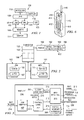
- Figure 1 shows a diagram of a system in accordance with preferred embodiments of the invention and including a Java Stack Machine ("JSM") and a Main Processor Unit ("MPU");
- Figure 2 shows illustrates the use of a translation lookaside buffer ("TLB") incorporating a task identifier field to permit selective TLB flushing;
- Figure 3 shows a preferred embodiment using a synchronization logic unit coupled to the JSM and MPU;
- Figure 4 shows an alternative embodiment using a synchronization logic unit coupled to the JSM and MPU;
- Figure 5 shows a block diagram of the synchronization unit used in the embodiments of Figures 3 and 4; and
- Figure 6 depicts an exemplary embodiment of the system described herein in the form of a communication device (e.g., cellular telephone).
-
- The following discussion is directed to various embodiments of the invention. Although one or more of these embodiments may be preferred, the embodiments disclosed should not be interpreted, or otherwise used, as limiting the scope of the disclosure, including the claims, unless otherwise specified. In addition, one skilled in the art will understand that the following description has broad application, and the discussion of any embodiment is meant only to be exemplary of that embodiment, and not intended to intimate that the scope of the disclosure, including the claims, is limited to that embodiment.
- Referring now to Figure 1, a
system 100 is shown in accordance with a preferred embodiment of the invention. As shown, the system includes at least twoprocessors Processor 102 comprises the Java optimized processor and is referred to for purposes of this disclosure as a Java Stack Machine ("JSM").Processor 104 is referred to as a Main Processor Unit ("MPU") and preferably is a RISC processor.System 100 also may includememory 106 coupled to both the JSM 102 and MPU 104 and thus is accessible by both processors. At least a portion of thememory 106 may be shared by both processors meaning that both processors may access the same shared memory locations. Further, if desired, a portion of thememory 106 may be designated as private to one processor or the other.System 100 also includes a Java Virtual Machine ("JVM") 108,compiler 110, and adisplay 114. The JSM 102 preferably includes an interface to one or more input/output ("I/O") devices such as a keypad to permit a user to control various aspects of thesystem 100. In addition, data streams may be received from the I/O space into the JSM 102 to be processed by the JSM 102. Other components (not specifically shown) may be included as desired. - Referring still to Figure 1, as is generally known, Java code comprises a plurality of "Bytecodes" 112.
Bytecodes 112 may be provided to the JVM 108, compiled bycompiler 110 and provided to the JSM 102 and/or MPU 104 for execution therein. In accordance with a preferred embodiment of the invention, the JSM 102 may execute at least some, and generally most, of the Java Bytecodes. When appropriate, however, the JSM 102 may request the MPU 104 to execute one or more Java Bytecodes not executed or executable by the JSM 102. In addition to executing Java Bytecodes, the MPU 104 also may execute non-Java instructions. The MPU 104 also hosts an operating system ("O/S") 105, which performs various functions including system memory management, the system task management that schedules theJVM 108 and most or all other native tasks running on the system, management of thedisplay 114, receiving input from input devices, etc. The O/S 105 preferably runs exclusively on the MPU 104 and thus does not run on the JSM 102 or other processors, if included. Without limitation, Java code may be used to perform any one of a variety of applications including multimedia, games or web based applications in thesystem 100, while non-Java code, which may comprise the O/S and other native applications, may still run on the system on theMPU 104. - The JVM 108 generally comprises a combination of software and hardware. The software may include the
compiler 110 and the hardware may include the JSM 102. The JVM may include a class loader, bytecode verifier, garbage collector, and a bytecode interpreter loop to interpret the bytecodes that are not executed on the JSMprocessor 102. - Figure 1 thus illustrates a multi-processor system having in which an operating system is executed exclusively on one of the processors. In at least this way, the system is asymmetric. With only one processor running an operating system several advantages are obtained over multi-processor systems having an operating system running on each processor. For example, in a multi-operating system environment, coordination between operating system instances is problematic and may result in an undesirable amount of latency with regard to inter-processor communication. The multi-processor, single O/S implementation described herein generally results in lower communication overhead and lower complexity than distributed operating system systems. Additionally, the single O/S configuration described herein may result in lower code size than in multiple O/S configurations. The following description addresses various features useful to implement the multi-processor, single O/S system of the preferred embodiment. The features described below comprise the ability to selectively flush a shared translation lookaside buffer and synchronization logic used to synchronize the JSM 102 and MPU 104.
- In Figure 2, the JSM 102 and MPU 104 are shown coupled to a shared translation lookaside buffer ("TLB") 150. The TLB 150 preferably is implemented in a storage device that may be separate from
memory 106. The TLB 150 preferably includes a plurality ofentries 152 in which virtual address to physical address translations are stored. Eachentry 152 thus includes avirtual address 162 and a correspondingphysical address 164. Each TLB entry may include a task identifier ("task ID") 160 and aV field 166. Other fields also may be included in the TLB entries, but are not shown in Figure 2. TheTLB 150 may be programmed in any suitable manner. For instance, as described in copending application 10/157,555 entitled "Cache With Selective Write Allocation", a memory transaction resulting in a TLB miss may initiate a TLB handler routine to load the missing reference into the TLB. - Each
processor - On a micro-TLB miss, the shared
TLB 150 is searched. In the case of a hit on the sharedTLB 150, the micro-TLB that missed is loaded with the entry content of the shared TLB. In the case of a miss in the sharedTLB 150, a TLB handler loads the relevant entry into the shared TLB and the micro-TLB that initially missed. - Referring still to Figure 2, each TLB entry preferably contains a
task ID field 160. Each processor also contains atask ID register processors task ID register JSM 102 and the tasks that have run on theMPU 104. In a JAVA environment, theJVM 108, for instance, may write the JVM task ID register with a value corresponding to the JVM task ID on theMPU 104, so that the O/S sees all JAVA tasks with the same ID. - The information in this table permits the O/S running on the
MPU 104 to selectively flush the entries in the sharedTLB 150. Flushing a TLB entry refers to invalidating the entry by clearing a valid bit inV field 166. Flushing one or more TLB entries may be desirable when switching contexts. Rather than being forced to flush all of the entries in the shared TLB, the O/S may flush only the entries relevant to tasks running on theMPU 104 or only entries relevant to tasks running on theJSM 102. The selection of which entries to flush preferably is based on the task ID values. For instance, if tasks 1, 3 and 5 are assigned to theJSM 102 and tasks 2, 4, and 6 are assigned to theMPU 104, the O/S can issue a command to flush only those entries in theTLB 150 whosetask identifier field 160 contains the task ID 2, 4 or 6. All other TLB entries will remain unchanged. With the O/S selectively flushing, for example, only the tasks associated with theMPU 104, the performance impact to theJSM 102, which would otherwise result if the entire TLB was invalidated, is reduced or eliminated. - In other embodiments, middle layer software may be responsible for selectively flushing the shared
TLB 150. An example of such middle layer software is theJVM 108. - As described above, the shared
TLB 150 can be selectively flushed based on task ID. In general, a micro-TLB only contains translations relevant to the processor in which the micro-TLB resides. As such, the selective flushing feature of the sharedTLB 150 need not be extended to the micro-TLBs. However, in alternate embodiments, one or more micro-TLB may have translations pertaining to multiple processors. In this case, the selective flushing technique may be applied to such a micro-TLB by including a task ID field to each micro-TLB entry. - In some situations, it may be desired for a processor to switch its "context." Switching context generally comprises one or more actions such as saving the current state of some or all registers so that new threads may run on the processor with new address translations. In accordance with a preferred embodiment, the
JSM 102 can switch its own context when triggered by theMPU 104 without further assistance from the MPU. The ability of theJSM 102 to autonomously switch context reduces latency induced onMPU 104 so that the overhead impact on the O/S due to the attached processor context switches is limited. - Figures 3-5 illustrate various techniques usable to synchronize the operation of multiple processors in a
system 200. As shown, thesystem 200 may comprise theJSM 102, theMPU 104, asynchronization unit 206, atransaction bus 208,memory 106, and a variety of signals such as await signal 212, await release 214, system interrupts 209, a system interrupt detectsignal 216, and a processor interrupt 218. Other components (not shown) may be included as well. Thesynchronization logic 206 synchronizes theprocessors - In operation, the
MPU 104 performs memory accesses through atransaction bus 208 tomemory 106. These accesses may include read or write cycles targeting various locations inmemory 106. Thetransaction bus 208 preferably is also provided tosynchronization unit 206, thereby permitting thesynchronization unit 206 to monitor transactions that target one or more pre-determined addresses as will be explained below. - In accordance with the preferred embodiments, at least one address (or a range of addresses) is selected or otherwise pre-determined to be used to place the
MPU 104 in a "wait" mode. The wait mode is generally specific to the particular processor selected asprocessor 104 and may include a lower performance or lower power mode in which, for example, one or more clocks internal to theprocessor 104 are disabled. The pre-determined address preferably is mapped to a physical memory location and thus can be used as a mechanism for initiating the MPU's transition to the wait mode. To initiate the transition to the wait mode, theMPU 104 preferably performs a read or write access targeting the address pre-determined for use for this purpose. As such, when thesynchronization unit 206 detects an access ontransaction bus 208, thesynchronization unit 206 determines whether the access is for the pre-determined address. Thesynchronization unit 206 responds to the detection of the access having the pre-determined address by assertingwait signal 212 to theMPU 104. - In another embodiment, instead of mapping this transaction to a physical address, the transaction could be mapped on a dedicated communication bus (i.e., a co-processor bus) between the
MPU 104 and theJSM 102, whereby a transaction to the specific address of the communication bus or a specific command on the communication bus performs the same function as addressing a physical memory address While theMPU 104 is in a wait mode, theJSM 102 may execute instructions or otherwise be occupied. TheJSM 102 may encounter an instruction that requires support from, or at least benefits from support by, theMPU 104. Accordingly, theJSM 102 may assert await release signal 214 to thesynchronization unit 206, thereby causing thesynchronization unit 206 to de-assert thewait signal 212. Once thewait signal 212 is de-asserted as described below, theMPU 104 can execute the instruction for which theJSM 102 needed support.
In at least some embodiments, upon "waking up," theMPU 104 preferably requests a status from theJSM 102. The status may include, without limitation, one or more status bits of aregister 205 that indicate whether theJSM 102 is actively executing instructions and identify any instruction(s) that theMPU 104 is to execute. - In addition to being awoken by the assertion of the
wait release signal 214 by theJSM 102, theMPU 104 may be awoken by a system interrupt 209. The system interrupt 209 may be sent to theMPU 104, which asserts a system interrupt detectsignal 216 to thesynchronization unit 206 to cause the de-assertion of thewait signal 212. The system interrupt 209 may be sent by a variety of system components (not shown), for example, I/O devices, timers, etc., to allow theMPU 104 to carry out, for example, routine maintenance, such as memory allocation and de-allocation, and other operations as desired. - After finishing the task prompted by the system interrupt 209, the
MPU 104 may read the status of theJSM 102. If theJSM 102 is in an idle state (i.e., theJSM 102 is not actively executing instructions), theMPU 104 may execute one or more instructions one behalf of theJSM 102. As previously described, theJSM 102 may encounter an instruction that requires, or at least benefits from, the support of theMPU 104. Thus, this instruction may be executed by theMPU 104. If theJSM 102 is not in an idle state, theMPU 104 may transition to a wait mode again as previously described (i.e., by executing a memory access to a pre-determined address detectable by the synchronization unit 206). - In at least some embodiments of the invention, the
MPU 104 may prioritize multiple tasks when awake. For example, if theMPU 104 has been awoken by a system interrupt 209, more than one interrupt source may have positioned the system interrupt 209 and the MPU will perform the associated tasks according to their pre-determined priority. In at least some embodiments, an operating system ("O/S") running of theMPU 104 may control the order in which theMPU 104 carries out multiple interrupt requests. - In some situations, for example, when a system interrupt 209 has awoken the
MPU 104 as described above, theJSM 102 may be unaware that theMPU 104 has awoken. In this situation theJSM 102 may assert the wait release signal 214 as described above to obtain processing support from theMPU 104. Assertion of the wait release signal in this context causes thesynchronization unit 206 to assert a processor interruptsignal 218 to theMPU 104. The asserted processor interruptsignal 218 preferably causes the MPU to temporarily stop executing a task, e.g. a routine maintenance task initiated upon occurrence of a system interrupt 209, to execute instructions as requested by theJSM 102. In other embodiments, the processor interruptsignal 218 is not used and any request by theJSM 102 is handled after theMPU 104 has finished the task(s) initiated by a system interrupt 209. - In embodiments in which multiple signals (e.g. system interrupt 209, system interrupt detect 216, wait release 214) occur simultaneously, approximately simultaneously, or concurrently, the operating system ("O/S") running on the
MPU 104 may decide, according to a pre-determined priority, whether theMPU 104 will execute instructions as requested by theJSM 102 or execute the task(s) requested by the system interrupt 209. As shown in Figure 6, the processor interruptsignal 218 asserted by thesynchronization unit 206 as described above may be received by theMPU 104 as a system interrupt 209 and handled according to a pre-determined priority. More specifically, the embodiment described above enables the O/S running on theMPU 104 to schedule multiple types of support requests from theJSM 102 relative to their respective priority as compared to other requests (e.g., system interrupts 209) handled by the MPU. Some of the support requests from theJSM 102 may have lower priority than some system interrupts 209, while other support requests from theJSM 102 have a higher priority. The priority of a support request from theJSM 102 may be included in the status read by theMPU 104 as described above. The processor interrupt may itself contain the priority information as well. - Figure 4 is a diagram illustrating another embodiment of the invention. As shown in Figure 4,
system 201 comprises the same components and signals assystem 200 of Figure 3, with the addition of a system interruptcontroller 207. The system interruptcontroller 207 preferably receives the processor interruptsignal 218 from thesynchronization unit 206 and request signals 238 from system components (e.g., I/O devices 231,timers 232, or other devices), and asserts the system interrupt detect 216 signal to thesynchronization unit 206 and the system interruptsignal 209 to theMPU 104. The function of the components and signals ofsystem 201 is otherwise described above forsystem 200. - Figure 5 is a block diagram illustrating an embodiment of the
synchronization unit 206. As shown in Figure 5, thesynchronization unit 206 may comprise adecode logic unit 203, aMPU interface 205, aJSM interface 207, a system interruptinterface 209, andcontrol logic 211. Thecontrol logic 211 preferably couples to theMPU interface 205, theJSM interface 207, and the system interruptinterface 209 as shown. Transaction information 213 (e.g., address, clock, or other information as may be helpful to detect that a transaction has been or is in the process of being made) received throughtransaction bus 208 preferably is provided by theMPU interface 205 to thedecode logic unit 203. - The
decode logic unit 203 detects a transaction targeting a pre-determined address that is initiated by the MPU as described above. For example, if the transaction is detected by recognizing that a pre-determined address has been or is to be accessed, thedecode logic unit 203 may assert an address detect signal 236 to thecontrol logic 211 when the transaction bus address matches the pre-determined address or falls within a pre-determined range of addresses. Upon detecting the assertion of the address detectsignal 215, control logic 211preferably asserts thewait signal 212 which is propagated via theMPU interface 205 to the MPU as described above. Thecontrol logic 211 may assert, or not, the wait signal when it receives an address detectsignal 215 depending on the state of thewait release signal 214 and the system interruptsignal 216. - Referring still to Figure 5, the
JSM interface 207 may be used to receive a wait release signal 214 from the JSM as explained above. TheJSM interface 207 may then propagate thewait release signal 214 to thecontrol logic 211. If thewait signal 212 is already de-asserted when await release signal 214 is received, a processor interruptsignal 218 may be asserted. More specifically, thecontrol logic 211 may assert, or not, the processor interruptsignal 218 when it receives await release signal 214 depending on the state of the address detectsignal 215 and the state of thewait signal 212. As explained above, the processor interrupt 218 may permit the MPU to temporarily stop executing a task, in order to execute one or more instructions for theJSM 102.
The system interruptinterface 209 receives the system interrupt detect signal 216 from the MPU or system interrupt controller and propagates the system interrupt detectsignal 216 to thecontrol logic 211. Thecontrol logic 211 may de-assert thewait signal 212 when it receives thewait release signal 214 and/or the system interrupt detectsignal 216. As previously described, the assertion and de-assertion of thewait signal 212 causes a processor to enter or wake up from a wait mode. In at least some embodiments, thecontrol logic 211 may receive inputs, e.g., system interrupt detect 216, address detectsignal 215, waitrelease signal 214, etc., and accordingly asserts or de-asserts thewait signal 212. - As described above, the
synchronization unit 206 may be used in combination with the JSM andMPU processors synchronization unit 206 may function to synchronize the operation of the JSM and MPU to permit efficient switching between such processors. Thesynchronization unit 206 which is shown as a separate unit in Figures 3 and 4, may be included as part of theJSM 102 in some embodiments of the invention. -
System 100 may be representative of, or adapted to, a wide variety of electronic systems, an exemplary electronic system may comprise a battery-operated, mobile cell phone such as that shown in Figure 6. As shown in Figure 6, a mobile communications device includes anintegrated keypad 412 anddisplay 414. TheJSM 102 andMPU 104 noted above and other components may be included inelectronics package 410 which may be coupled tokeypad 410,display 414, and radio frequency ("RF")circuitry 416 which may be connected to anantenna 418. - While the preferred embodiments of the present invention have been shown and described, modifications thereof can be made by one skilled in the art without departing from the spirit and teachings of the invention. The embodiments described herein are exemplary only, and are not intended to be limiting. Many variations and modifications of the invention disclosed herein are possible and are within the scope of the invention. Accordingly, the scope of protection is not limited by the description set out above. Each and every claim is incorporated into the specification as an embodiment of the present invention.
Claims (19)
Priority Applications (2)
| Application Number | Priority Date | Filing Date | Title |
|---|---|---|---|
| EP03291926A EP1391820A3 (en) | 2002-07-31 | 2003-07-30 | Concurrent task execution in a multi-processor, single operating system environment |
| US10/632,077 US7716673B2 (en) | 2002-07-31 | 2003-07-31 | Tasks distribution in a multi-processor including a translation lookaside buffer shared between processors |
Applications Claiming Priority (3)
| Application Number | Priority Date | Filing Date | Title |
|---|---|---|---|
| US40039102P | 2002-07-31 | 2002-07-31 | |
| US400391P | 2002-07-31 | ||
| EP03291926A EP1391820A3 (en) | 2002-07-31 | 2003-07-30 | Concurrent task execution in a multi-processor, single operating system environment |
Publications (2)
| Publication Number | Publication Date |
|---|---|
| EP1391820A2 true EP1391820A2 (en) | 2004-02-25 |
| EP1391820A3 EP1391820A3 (en) | 2007-12-19 |
Family
ID=39185839
Family Applications (1)
| Application Number | Title | Priority Date | Filing Date |
|---|---|---|---|
| EP03291926A Ceased EP1391820A3 (en) | 2002-07-31 | 2003-07-30 | Concurrent task execution in a multi-processor, single operating system environment |
Country Status (2)
| Country | Link |
|---|---|
| US (1) | US7716673B2 (en) |
| EP (1) | EP1391820A3 (en) |
Cited By (1)
| Publication number | Priority date | Publication date | Assignee | Title |
|---|---|---|---|---|
| US9886392B2 (en) | 2014-03-20 | 2018-02-06 | International Business Machines Corporation | Selective purging of PCI I/O address translation buffer |
Families Citing this family (47)
| Publication number | Priority date | Publication date | Assignee | Title |
|---|---|---|---|---|
| US7392524B2 (en) * | 2004-04-06 | 2008-06-24 | International Business Machines Corporation | Method, system, and storage medium for managing computer processing functions |
| JP2008522277A (en) * | 2004-11-30 | 2008-06-26 | コーニンクレッカ フィリップス エレクトロニクス エヌ ヴィ | Efficient switching between prioritized tasks |
| US20060184713A1 (en) * | 2005-02-16 | 2006-08-17 | Hob Gmbh & Co. Kg | Method for operating a virtual machine computer system running guest operating systems on a central processing means virtualized by a host system having register stack engine functionality |
| US7386669B2 (en) * | 2005-03-31 | 2008-06-10 | International Business Machines Corporation | System and method of improving task switching and page translation performance utilizing a multilevel translation lookaside buffer |
| US7398371B2 (en) * | 2005-06-23 | 2008-07-08 | Qualcomm Incorporated | Shared translation look-aside buffer and method |
| US7616218B1 (en) * | 2005-12-05 | 2009-11-10 | Nvidia Corporation | Apparatus, system, and method for clipping graphics primitives |
| US7509472B2 (en) * | 2006-02-01 | 2009-03-24 | Sun Microsystems, Inc. | Collapsible front-end translation for instruction fetch |
| US20070256076A1 (en) * | 2006-04-27 | 2007-11-01 | Thompson James W | System and method for separating multiple workloads processing in a single computer operating environment |
| US8769703B2 (en) * | 2006-04-27 | 2014-07-01 | Unisys Corporation | System and method for providing a mechanism to virtualize a perpetual, unique system identity on a partitioned computer system |
| US8352709B1 (en) | 2006-09-19 | 2013-01-08 | Nvidia Corporation | Direct memory access techniques that include caching segmentation data |
| US8601223B1 (en) | 2006-09-19 | 2013-12-03 | Nvidia Corporation | Techniques for servicing fetch requests utilizing coalesing page table entries |
| US8347064B1 (en) | 2006-09-19 | 2013-01-01 | Nvidia Corporation | Memory access techniques in an aperture mapped memory space |
| US8543792B1 (en) | 2006-09-19 | 2013-09-24 | Nvidia Corporation | Memory access techniques including coalesing page table entries |
| US8700883B1 (en) | 2006-10-24 | 2014-04-15 | Nvidia Corporation | Memory access techniques providing for override of a page table |
| US8707011B1 (en) | 2006-10-24 | 2014-04-22 | Nvidia Corporation | Memory access techniques utilizing a set-associative translation lookaside buffer |
| US8533425B1 (en) | 2006-11-01 | 2013-09-10 | Nvidia Corporation | Age based miss replay system and method |
| US8706975B1 (en) | 2006-11-01 | 2014-04-22 | Nvidia Corporation | Memory access management block bind system and method |
| US8504794B1 (en) | 2006-11-01 | 2013-08-06 | Nvidia Corporation | Override system and method for memory access management |
| US8607008B1 (en) | 2006-11-01 | 2013-12-10 | Nvidia Corporation | System and method for independent invalidation on a per engine basis |
| US8347065B1 (en) | 2006-11-01 | 2013-01-01 | Glasco David B | System and method for concurrently managing memory access requests |
| US8700865B1 (en) | 2006-11-02 | 2014-04-15 | Nvidia Corporation | Compressed data access system and method |
| US7631147B2 (en) * | 2006-12-06 | 2009-12-08 | Microsoft Corporation | Efficient flushing of translation lookaside buffers in a multiprocessor environment |
| US8161482B1 (en) * | 2007-04-13 | 2012-04-17 | Marvell International Ltd. | Power optimization for multi-core devices |
| US8146087B2 (en) * | 2008-01-10 | 2012-03-27 | International Business Machines Corporation | System and method for enabling micro-partitioning in a multi-threaded processor |
| CN101782862B (en) * | 2009-01-16 | 2013-03-13 | 鸿富锦精密工业(深圳)有限公司 | Processor distribution control system and control method thereof |
| US9979589B2 (en) | 2009-12-10 | 2018-05-22 | Royal Bank Of Canada | Coordinated processing of data by networked computing resources |
| US9940670B2 (en) | 2009-12-10 | 2018-04-10 | Royal Bank Of Canada | Synchronized processing of data by networked computing resources |
| US9959572B2 (en) | 2009-12-10 | 2018-05-01 | Royal Bank Of Canada | Coordinated processing of data by networked computing resources |
| CA2927607C (en) | 2009-12-10 | 2021-04-06 | Royal Bank Of Canada | Synchronized processing of data by networked computing resources |
| US10057333B2 (en) | 2009-12-10 | 2018-08-21 | Royal Bank Of Canada | Coordinated processing of data by networked computing resources |
| US8751833B2 (en) * | 2010-04-30 | 2014-06-10 | Arm Limited | Data processing system |
| US8856775B2 (en) * | 2010-09-22 | 2014-10-07 | International Business Machines Corporation | Unstacking software components for migration to virtualized environments |
| US10146545B2 (en) | 2012-03-13 | 2018-12-04 | Nvidia Corporation | Translation address cache for a microprocessor |
| US9880846B2 (en) | 2012-04-11 | 2018-01-30 | Nvidia Corporation | Improving hit rate of code translation redirection table with replacement strategy based on usage history table of evicted entries |
| US10241810B2 (en) | 2012-05-18 | 2019-03-26 | Nvidia Corporation | Instruction-optimizing processor with branch-count table in hardware |
| US20140101405A1 (en) * | 2012-10-05 | 2014-04-10 | Advanced Micro Devices, Inc. | Reducing cold tlb misses in a heterogeneous computing system |
| US20140189310A1 (en) | 2012-12-27 | 2014-07-03 | Nvidia Corporation | Fault detection in instruction translations |
| US10108424B2 (en) | 2013-03-14 | 2018-10-23 | Nvidia Corporation | Profiling code portions to generate translations |
| GB2529394A (en) | 2014-08-14 | 2016-02-24 | Ibm | Multiprocessor computer system |
| US9672159B2 (en) * | 2015-07-02 | 2017-06-06 | Arm Limited | Translation buffer unit management |
| US10452566B2 (en) * | 2015-10-02 | 2019-10-22 | Nvidia Corporation | Storing secure state information in translation lookaside buffer cache lines |
| US9892058B2 (en) * | 2015-12-16 | 2018-02-13 | Advanced Micro Devices, Inc. | Centrally managed unified shared virtual address space |
| US9798597B1 (en) * | 2016-09-26 | 2017-10-24 | International Business Machines Corporation | Verifying selective purging of entries from translation look-aside buffers |
| US10606488B2 (en) * | 2017-06-30 | 2020-03-31 | Intel Corporation | Selective data flush in a storage device |
| US10970118B2 (en) | 2017-08-02 | 2021-04-06 | Advanced Micro Devices, Inc. | Shareable FPGA compute engine |
| US11422812B2 (en) | 2019-06-25 | 2022-08-23 | Advanced Micro Devices, Inc. | Method and apparatus for efficient programmable instructions in computer systems |
| US11513963B2 (en) * | 2021-03-11 | 2022-11-29 | Western Digital Technologies. Inc. | Data storage device and method for application identifier handler heads-up for faster storage response |
Citations (2)
| Publication number | Priority date | Publication date | Assignee | Title |
|---|---|---|---|---|
| EP1182570A2 (en) | 2000-08-21 | 2002-02-27 | Texas Instruments Incorporated | TLB with resource ID field |
| US20020062047A1 (en) | 2000-09-28 | 2002-05-23 | Nippon Shokubai Co., Ltd. | Process for producing 2,4,5,-trialkylbenzaldehydes |
Family Cites Families (28)
| Publication number | Priority date | Publication date | Assignee | Title |
|---|---|---|---|---|
| US4638426A (en) * | 1982-12-30 | 1987-01-20 | International Business Machines Corporation | Virtual memory address translation mechanism with controlled data persistence |
| JP2510605B2 (en) * | 1987-07-24 | 1996-06-26 | 株式会社日立製作所 | Virtual computer system |
| JPH0679307B2 (en) * | 1987-10-22 | 1994-10-05 | 日本電気株式会社 | Coprocessor parallel operation control method |
| US5210828A (en) * | 1988-12-29 | 1993-05-11 | International Business Machines Corporation | Multiprocessing system with interprocessor communications facility |
| US5787476A (en) * | 1995-05-05 | 1998-07-28 | Silicon Graphics, Inc. | System and method for maintaining coherency of virtual-to-physical memory translations in a multiprocessor computer |
| US5809522A (en) * | 1995-12-18 | 1998-09-15 | Advanced Micro Devices, Inc. | Microprocessor system with process identification tag entries to reduce cache flushing after a context switch |
| US6006320A (en) * | 1996-07-01 | 1999-12-21 | Sun Microsystems, Inc. | Processor architecture with independent OS resources |
| US5940872A (en) * | 1996-11-01 | 1999-08-17 | Intel Corporation | Software and hardware-managed translation lookaside buffer |
| US6098089A (en) | 1997-04-23 | 2000-08-01 | Sun Microsystems, Inc. | Generation isolation system and method for garbage collection |
| US6260131B1 (en) * | 1997-11-18 | 2001-07-10 | Intrinsity, Inc. | Method and apparatus for TLB memory ordering |
| US6029000A (en) * | 1997-12-22 | 2000-02-22 | Texas Instruments Incorporated | Mobile communication system with cross compiler and cross linker |
| GB9907283D0 (en) | 1999-03-31 | 1999-05-26 | Koninkl Philips Electronics Nv | Memory reclamation method |
| US6668275B1 (en) * | 1999-12-17 | 2003-12-23 | Honeywell International Inc. | System and method for multiprocessor management |
| US7028299B1 (en) * | 2000-06-30 | 2006-04-11 | Intel Corporation | Task-based multiprocessing system |
| JP2002041489A (en) * | 2000-07-25 | 2002-02-08 | Mitsubishi Electric Corp | Synchronous signal generation circuit, processor system using the same, and synchronous signal generation method |
| US6742103B2 (en) * | 2000-08-21 | 2004-05-25 | Texas Instruments Incorporated | Processing system with shared translation lookaside buffer |
| EP1182562B1 (en) | 2000-08-21 | 2011-05-11 | Texas Instruments France | Smartcache with interruptible block prefetch |
| EP1213650A3 (en) * | 2000-08-21 | 2006-08-30 | Texas Instruments France | Priority arbitration based on current task and MMU |
| EP1182559B1 (en) * | 2000-08-21 | 2009-01-21 | Texas Instruments Incorporated | Improved microprocessor |
| US6742104B2 (en) * | 2000-08-21 | 2004-05-25 | Texas Instruments Incorporated | Master/slave processing system with shared translation lookaside buffer |
| EP1182565B1 (en) | 2000-08-21 | 2012-09-05 | Texas Instruments France | Cache and DMA with a global valid bit |
| US6567905B2 (en) | 2001-01-23 | 2003-05-20 | Gemstone Systems, Inc. | Generational garbage collector with persistent object cache |
| EP1304620A1 (en) | 2001-10-17 | 2003-04-23 | Texas Instruments Incorporated | Cache with selective write allocation |
| US6976254B2 (en) * | 2001-11-28 | 2005-12-13 | Esmertec Ag | Inter-method control transfer for execution engines with memory constraints |
| AU2002365812A1 (en) * | 2001-12-04 | 2003-06-17 | Powerllel Corporation | Parallel computing system, method and architecture |
| US7137121B2 (en) * | 2002-04-19 | 2006-11-14 | Equator Technologies, Inc. | Data-processing circuit and method for switching between application programs without an operating system |
| US7318127B2 (en) * | 2005-02-11 | 2008-01-08 | International Business Machines Corporation | Method, apparatus, and computer program product for sharing data in a cache among threads in an SMT processor |
| US7624248B1 (en) * | 2006-04-14 | 2009-11-24 | Tilera Corporation | Managing memory in a parallel processing environment |
-
2003
- 2003-07-30 EP EP03291926A patent/EP1391820A3/en not_active Ceased
- 2003-07-31 US US10/632,077 patent/US7716673B2/en active Active
Patent Citations (2)
| Publication number | Priority date | Publication date | Assignee | Title |
|---|---|---|---|---|
| EP1182570A2 (en) | 2000-08-21 | 2002-02-27 | Texas Instruments Incorporated | TLB with resource ID field |
| US20020062047A1 (en) | 2000-09-28 | 2002-05-23 | Nippon Shokubai Co., Ltd. | Process for producing 2,4,5,-trialkylbenzaldehydes |
Cited By (3)
| Publication number | Priority date | Publication date | Assignee | Title |
|---|---|---|---|---|
| US9886392B2 (en) | 2014-03-20 | 2018-02-06 | International Business Machines Corporation | Selective purging of PCI I/O address translation buffer |
| US9886391B2 (en) | 2014-03-20 | 2018-02-06 | International Business Machines Corporation | Selective purging of PCI I/O address translation buffer |
| US10223283B2 (en) | 2014-03-20 | 2019-03-05 | International Business Machines Corporation | Selective purging of PCI I/O address translation buffer |
Also Published As
| Publication number | Publication date |
|---|---|
| EP1391820A3 (en) | 2007-12-19 |
| US7716673B2 (en) | 2010-05-11 |
| US20040025161A1 (en) | 2004-02-05 |
Similar Documents
| Publication | Publication Date | Title |
|---|---|---|
| US7716673B2 (en) | Tasks distribution in a multi-processor including a translation lookaside buffer shared between processors | |
| US6769052B2 (en) | Cache with selective write allocation | |
| EP1182559B1 (en) | Improved microprocessor | |
| US6738888B2 (en) | TLB with resource ID field | |
| US6728800B1 (en) | Efficient performance based scheduling mechanism for handling multiple TLB operations | |
| US6957315B2 (en) | TLB lock and unlock operation | |
| US20060026322A1 (en) | Interrupt management in dual core processors | |
| US8032716B2 (en) | System, method and computer program product for providing a new quiesce state | |
| US8332614B2 (en) | System, method and computer program product for providing a programmable quiesce filtering register | |
| US20260093635A1 (en) | Translation lookaside buffer prewarming | |
| US20090217269A1 (en) | System, method and computer program product for providing multiple quiesce state machines | |
| JPH10124202A (en) | Method and system for reducing power consumption in electronic circuits | |
| US7712098B2 (en) | Data transfer controlled by task attributes | |
| US20020062434A1 (en) | Processing system with shared translation lookaside buffer | |
| US8516502B2 (en) | Performing java interrupt with two program counters | |
| KR20060023963A (en) | Methods, apparatus, and systems for providing multithreaded computer processing | |
| EP1313014B1 (en) | Interruptible and re-entrant instruction for cleaning a region of a cache memory | |
| US7761686B2 (en) | Address translator and address translation method | |
| US20040024988A1 (en) | Synchronization of processor states | |
| US20040024991A1 (en) | Using IMPDEP2 for system commands related to Java accelator hardware | |
| US8429383B2 (en) | Multi-processor computing system having a JAVA stack machine and a RISC-based processor | |
| US7203797B2 (en) | Memory management of local variables | |
| US11080188B1 (en) | Method to ensure forward progress of a processor in the presence of persistent external cache/TLB maintenance requests | |
| US9043507B2 (en) | Information processing system | |
| US20040078528A1 (en) | Cache coherency in a multi-processor system |
Legal Events
| Date | Code | Title | Description |
|---|---|---|---|
| PUAI | Public reference made under article 153(3) epc to a published international application that has entered the european phase |
Free format text: ORIGINAL CODE: 0009012 |
|
| AK | Designated contracting states |
Kind code of ref document: A2 Designated state(s): AT BE BG CH CY CZ DE DK EE ES FI FR GB GR HU IE IT LI LU MC NL PT RO SE SI SK TR |
|
| AX | Request for extension of the european patent |
Extension state: AL LT LV MK |
|
| RAP1 | Party data changed (applicant data changed or rights of an application transferred) |
Owner name: TEXAS INSTRUMENTS FRANCE Owner name: TEXAS INSTRUMENTS INCORPORATED |
|
| RTI1 | Title (correction) |
Free format text: CONCURRENT TASK EXECUTION IN A MULTI-PROCESSOR, SINGLE OPERATING SYSTEM ENVIRONMENT |
|
| PUAL | Search report despatched |
Free format text: ORIGINAL CODE: 0009013 |
|
| AK | Designated contracting states |
Kind code of ref document: A3 Designated state(s): AT BE BG CH CY CZ DE DK EE ES FI FR GB GR HU IE IT LI LU MC NL PT RO SE SI SK TR |
|
| AX | Request for extension of the european patent |
Extension state: AL LT LV MK |
|
| 17P | Request for examination filed |
Effective date: 20080619 |
|
| AKX | Designation fees paid |
Designated state(s): DE FR GB |
|
| RBV | Designated contracting states (corrected) |
Designated state(s): DE FR GB NL |
|
| RAP1 | Party data changed (applicant data changed or rights of an application transferred) |
Owner name: TEXAS INSTRUMENTS FRANCE Owner name: TEXAS INSTRUMENTS INCORPORATED |
|
| 17Q | First examination report despatched |
Effective date: 20100614 |
|
| STAA | Information on the status of an ep patent application or granted ep patent |
Free format text: STATUS: THE APPLICATION HAS BEEN REFUSED |
|
| 18R | Application refused |
Effective date: 20151123 |