EP1390990B1 - Group iii nitride based semiconductor device with a multiple quantum well structure - Google Patents
Group iii nitride based semiconductor device with a multiple quantum well structure Download PDFInfo
- Publication number
- EP1390990B1 EP1390990B1 EP02726917A EP02726917A EP1390990B1 EP 1390990 B1 EP1390990 B1 EP 1390990B1 EP 02726917 A EP02726917 A EP 02726917A EP 02726917 A EP02726917 A EP 02726917A EP 1390990 B1 EP1390990 B1 EP 1390990B1
- Authority
- EP
- European Patent Office
- Prior art keywords
- layer
- group iii
- iii nitride
- layers
- quantum well
- Prior art date
- Legal status (The legal status is an assumption and is not a legal conclusion. Google has not performed a legal analysis and makes no representation as to the accuracy of the status listed.)
- Expired - Lifetime
Links
Images


Classifications
-
- H—ELECTRICITY
- H01—ELECTRIC ELEMENTS
- H01L—SEMICONDUCTOR DEVICES NOT COVERED BY CLASS H10
- H01L33/00—Semiconductor devices with at least one potential-jump barrier or surface barrier specially adapted for light emission; Processes or apparatus specially adapted for the manufacture or treatment thereof or of parts thereof; Details thereof
- H01L33/02—Semiconductor devices with at least one potential-jump barrier or surface barrier specially adapted for light emission; Processes or apparatus specially adapted for the manufacture or treatment thereof or of parts thereof; Details thereof characterised by the semiconductor bodies
- H01L33/04—Semiconductor devices with at least one potential-jump barrier or surface barrier specially adapted for light emission; Processes or apparatus specially adapted for the manufacture or treatment thereof or of parts thereof; Details thereof characterised by the semiconductor bodies with a quantum effect structure or superlattice, e.g. tunnel junction
- H01L33/06—Semiconductor devices with at least one potential-jump barrier or surface barrier specially adapted for light emission; Processes or apparatus specially adapted for the manufacture or treatment thereof or of parts thereof; Details thereof characterised by the semiconductor bodies with a quantum effect structure or superlattice, e.g. tunnel junction within the light emitting region, e.g. quantum confinement structure or tunnel barrier
-
- H—ELECTRICITY
- H01—ELECTRIC ELEMENTS
- H01L—SEMICONDUCTOR DEVICES NOT COVERED BY CLASS H10
- H01L21/00—Processes or apparatus adapted for the manufacture or treatment of semiconductor or solid state devices or of parts thereof
- H01L21/02—Manufacture or treatment of semiconductor devices or of parts thereof
- H01L21/02104—Forming layers
- H01L21/02365—Forming inorganic semiconducting materials on a substrate
- H01L21/02367—Substrates
- H01L21/0237—Materials
- H01L21/02373—Group 14 semiconducting materials
- H01L21/02378—Silicon carbide
-
- H—ELECTRICITY
- H01—ELECTRIC ELEMENTS
- H01L—SEMICONDUCTOR DEVICES NOT COVERED BY CLASS H10
- H01L21/00—Processes or apparatus adapted for the manufacture or treatment of semiconductor or solid state devices or of parts thereof
- H01L21/02—Manufacture or treatment of semiconductor devices or of parts thereof
- H01L21/02104—Forming layers
- H01L21/02365—Forming inorganic semiconducting materials on a substrate
- H01L21/02436—Intermediate layers between substrates and deposited layers
- H01L21/02439—Materials
- H01L21/02455—Group 13/15 materials
- H01L21/02458—Nitrides
-
- H—ELECTRICITY
- H01—ELECTRIC ELEMENTS
- H01L—SEMICONDUCTOR DEVICES NOT COVERED BY CLASS H10
- H01L21/00—Processes or apparatus adapted for the manufacture or treatment of semiconductor or solid state devices or of parts thereof
- H01L21/02—Manufacture or treatment of semiconductor devices or of parts thereof
- H01L21/02104—Forming layers
- H01L21/02365—Forming inorganic semiconducting materials on a substrate
- H01L21/02436—Intermediate layers between substrates and deposited layers
- H01L21/02494—Structure
- H01L21/02496—Layer structure
- H01L21/02505—Layer structure consisting of more than two layers
- H01L21/02507—Alternating layers, e.g. superlattice
-
- H—ELECTRICITY
- H01—ELECTRIC ELEMENTS
- H01L—SEMICONDUCTOR DEVICES NOT COVERED BY CLASS H10
- H01L21/00—Processes or apparatus adapted for the manufacture or treatment of semiconductor or solid state devices or of parts thereof
- H01L21/02—Manufacture or treatment of semiconductor devices or of parts thereof
- H01L21/02104—Forming layers
- H01L21/02365—Forming inorganic semiconducting materials on a substrate
- H01L21/02518—Deposited layers
- H01L21/02521—Materials
- H01L21/02538—Group 13/15 materials
- H01L21/0254—Nitrides
-
- H—ELECTRICITY
- H01—ELECTRIC ELEMENTS
- H01L—SEMICONDUCTOR DEVICES NOT COVERED BY CLASS H10
- H01L33/00—Semiconductor devices with at least one potential-jump barrier or surface barrier specially adapted for light emission; Processes or apparatus specially adapted for the manufacture or treatment thereof or of parts thereof; Details thereof
- H01L33/02—Semiconductor devices with at least one potential-jump barrier or surface barrier specially adapted for light emission; Processes or apparatus specially adapted for the manufacture or treatment thereof or of parts thereof; Details thereof characterised by the semiconductor bodies
- H01L33/26—Materials of the light emitting region
- H01L33/30—Materials of the light emitting region containing only elements of group III and group V of the periodic system
- H01L33/32—Materials of the light emitting region containing only elements of group III and group V of the periodic system containing nitrogen
-
- B—PERFORMING OPERATIONS; TRANSPORTING
- B82—NANOTECHNOLOGY
- B82Y—SPECIFIC USES OR APPLICATIONS OF NANOSTRUCTURES; MEASUREMENT OR ANALYSIS OF NANOSTRUCTURES; MANUFACTURE OR TREATMENT OF NANOSTRUCTURES
- B82Y20/00—Nanooptics, e.g. quantum optics or photonic crystals
Definitions
- This invention relates to microelectronic devices and fabrication methods therefor, and more particularly to structures which may be utilized in Group III nitride semiconductor devices, such as light emitting diodes (LEDs).
- LEDs light emitting diodes
- a light emitting diode generally includes a diode region on a microelectronic substrate.
- the microelectronic substrate may comprise, for example, gallium arsenide, gallium phosphide, alloys thereof, silicon carbide and/or sapphire.
- US-A-6,153,894 discloses technology for obtaining a shortwave light-emitting device made of a group-III nitride semiconductor crystal, and in particular, technology for fabricating a light-emitting layer which results in a high brightness luminescent light and in emission of a longer wavelength of light.
- the device comprises a light-emitting layer on a superlattice structure as a base layer, resulting in an improved crystallinity of the light-emitting layer.
- an abruptness of a crystal composition at the interface of the light-emitting layer and the upper junction layer is achieved, thus forming a bending portion of a band structure expedient for allowing the emitting-layer to emit a light with a long wavelength.
- US 6,153 , 894 discloses in particular a method of manufacturing a Group-III nitride-based semiconductor device having a multiple quantum well structure, comprising the steps of repeatedly forming a GaN barrier layer with a thickness of 20 nm and an InGaN quantum well layer with a thickness of 10 nm.
- WO 0076004 discloses a method of manufacturing a Group-III nitride-based semiconductor device having a multiple quantum well structure, comprising the steps of repeatedly forming a GaN barrier layer with a thickness of 20 nm at 800°C and an InGaN quantum well layer with a thickness of 3nm at 800°C.
- JP11040850 discloses a method of manufacturing a Group-III nitride-based semiconductor device having a multiple quantum well structure, comprising the steps of repeatedly forming a GaN barrier layer with a thickness of 3.5 nm at 900°C and an InGaN quantum well layer with a thickness of 3.5 nm at 600°C.
- Group III nitride based LEDs such as gallium nitride based LEDs
- gallium nitride LEDs have been fabricated on sapphire or silicon carbide substrates. Such substrates may result in mismatches between the crystal lattice of the substrate and the gallium nitride.
- Various techniques have been employed to overcome potential problems with the growth of gallium nitride on sapphire and/or silicon carbide. For example, aluminum nitride (AIN) may be utilized as a buffer between a silicon carbide substrate and a Group III active layer, particularly a gallium nitride active layer.
- aluminum nitride is insulating rather than conductive.
- structures with aluminum nitride buffer layers typically require shorting contacts that bypass the aluminum nitride buffer to electrically link the conductive silicon carbide substrate to the Group III nitride active layer.
- conductive buffer layer materials such as gallium nitride (GaN), aluminum gallium nitride (AlGaN), or combinations of gallium nitride and aluminum gallium nitride may allow for elimination of the shorting contacts typically utilized with AIN buffer layers. Typically, eliminating the shorting contact reduces the epitaxial layer thickness, decreases the number of fabrication steps required to produce devices, reduces the overall chip size, and/or increases the device efficiency. Accordingly, Group III nitride devices may be produced at lower cost with a higher performance. Nevertheless, although these conductive buffer materials offer these advantages, their crystal lattice match with silicon carbide is less satisfactory than is that of aluminum nitride.
- the present invention provides a Group III nitride-based semiconductor device having a multiple quantum well structure (18, 225) consisting of a periodically repeating quantum well structure (221) comprising:
- Embodiments of the present invention provide a light emitting diode having a Group III nitride based superlattice and a Group III nitride based active region on the superlattice.
- the active region has the multiple quantum well structure.
- the light emitting diode may include up to 10 repetitions of the quantum well structure.
- the superlattice includes a gallium nitride based superlattice having at least two periods of alternating layers of In x Ga 1-x N and In y Ga 1-y N, where 0 ⁇ X ⁇ 1 and 0 ⁇ Y ⁇ 1 and X is not equal to Y.
- the first Group III nitride based barrier layer provides a well support layer comprising a Group III nitride and the second Group III nitride based barrier layer provides a cap layer comprising a Group III nitride on the quantum well layer.
- the well support layer comprises a gallium nitride based layer
- the quantum well layer comprises an indium gallium nitride layer
- the barrier layer comprises a gallium nitride based layer.
- the well support layer and the cap layer may be provided by layers of In x Ga 1-x N where 0 ⁇ X.
- the indium composition of the well support layer and the cap layer may be provided by layers of In x Ga 1-x N where 0 ⁇ X.
- the well support layer comprises a gallium nitride based layer
- the quantum well layer comprises an indium gallium nitride layer
- the barrier layer comprises a gallium nitride based layer.
- the well support layer and the cap layer may be provided by layers of In x Ga 1-x N where 0 ⁇ X ⁇ 1.
- the indium composition of the well support layer and the cap layer may be less than the indium composition of the quantum well layer.
- the well support layer and the cap layer may also be provided by a layer of Al x In y Ga 1-x-y N where 0 ⁇ X ⁇ 1, 0 ⁇ Y ⁇ 1 and X+Y ⁇ 1. Furthermore, the well support layer and the cap layer may be undoped. Alternatively, the well support layer and the cap layer may have an n-type doping level of less than about 5x10 19 cm -3 . The cap layer and the well support layer may also have a higher bandgap than the quantum well layer.
- the combined thickness of the well support layer and the cap layer may be up to 40nm (400 ⁇ ). The thickness of the well support layer may be greater than a thickness of the cap layer.
- the quantum well layer may have a thickness of from 1 to 5 nm (10 to 50 ⁇ ). For example, the quantum well layer may have a thickness of about 2 nm (20 ⁇ ). Furthermore, the percentage of indium in the quantum well layer may be from 15% to 40%.
- a Group III nitride based spacer layer is provided between the well support layer and the superlattice.
- the spacer layer may be undoped GaN.
- the bandgap of the quantum well is less than the bandgap of the superlattice.
- the gallium nitride based superlattice comprises from 5 to 50 periods.
- the alternating layers of In x Ga 1-x N and In y Ga 1-y N may have a combined thickness of from 1 to 14 nm (10 to 140 ⁇ ).
- X 0 for layers of In x Ga 1-x N of the superlattice.
- the InGaN layers may have a thickness of from 0.5 to 4 nm (5 to 40 ⁇ ) and the GaN layers may have a thickness of from 0.5 to 10 nm (5 to 100 ⁇ ).
- the gallium nitride based superlattice is doped with an n-type impurity to a level of from 1x10 17 cm -3 to 5x10 19 cm -3 .
- the doping level of the gallium nitride based superlattice may be an actual doping level of layers of the alternating layers.
- the doping level may also be an average doping level of layers of the alternating layers.
- the light emitting diode may include doped Group III nitride layers adjacent the superlattice where the doped Group III nitride layers are doped with an n-type impurity to provide an average doping of the doped Group III nitride layers and the superlattice of from 1x10 17 cm -3 to 5x10 19 cm -3 .
- the bandgap of the superlattice may be from 2.95 eV to 3.35 eV and, in certain embodiments, may be about 3.15 eV.
- a Group III nitride based semiconductor device having an active region comprising a multiple quantum well structure according to claim 1 is provided.
- the quantum well structure includes a well support layer comprising a Group III nitride, a quantum well layer comprising a Group III nitride on the well support layer and a cap layer comprising a Group III nitride on the quantum well layer.
- the cap layer has a lower crystal quality than the well support layer.
- the well support layer may be provided by a gallium nitride based layer
- the quantum well layer may be provided by an indium gallium nitride layer
- the barrier layer may be provided by a gallium nitride based layer.
- the well support layer and the cap layer may be provided by layers of In X Ga 1-X N where 0 ⁇ X ⁇ 1.
- the indium composition of the well support layer and the cap layer may be less the indium composition of the quantum well layer.
- the well support layer and the cap layer may be provided by layers of Al X In Y Ga 1-X-Y N where 0 ⁇ X ⁇ 1, 0 ⁇ Y ⁇ 1 and X+Y ⁇ 1.
- the well support layer and the cap layer may be undoped.
- the well support layer and the cap layer may have a doping level of less than about 5x10 19 cm -3 .
- the cap layer and the well support layer have a higher bandgap than the quantum well layer.
- the combined thickness of the well support layer and the cap layer may be up to 40 nm (400 ⁇ ,), typically about 22.5 nm (225 ⁇ .).
- the thickness of the well support layer may be greater than the thickness of the cap layer.
- the quantum well layer has a thickness of from about 1 to 5 nm (10 to about 50 ⁇ .).
- the quantum well layer may have a thickness of about 2.5 nm (25 ⁇ .).
- the percentage of indium in the quantum well layer may from about 5% to about 50%.
- a superlattice is provided and the well support layer is on the superlattice.
- the superlattice may have a bandgap of about 3.15 eV.
- a Group III nitride based spacer layer may be provided between the well support layer and the superlattice.
- the spacer layer may be undoped GaN.
- the bandgap of the at least one quantum well may be less than the bandgap of the superlattice.
- a second well support layer comprising a Group III nitride is provided on the cap layer.
- a second quantum well layer comprising a Group III nitride is provided on the second well support layer; and a second cap layer comprising a Group III nitride is provided on the second quantum well layer.
- the Group III nitride based semiconductor device includes up to 10 repetitions of the quantum well structures.
- Embodiments of the present invention further provide a Group III nitride based semiconductor device that includes a gallium nitride based superlattice having at least two periods of alternating layers of In X Ga 1-X N and In Y Ga 1-Y N, where 0 ⁇ X ⁇ 1 and 0 ⁇ Y ⁇ 1 and X is not equal to Y.
- the gallium nitride based superlattice includes from 5 to 50 periods.
- the gallium nitride based superlattice may include 25 periods.
- the gallium nitride based superlattice may include 10 periods.
- the gallium nitride based superlattice comprises from 5 to 50 periods.
- the alternating layers of In X Ga 1-X N and In Y Ga 1-Y N may have a combined thickness of from 10 to 140 ⁇ .
- X 0 for layers of In X Ga 1-X N of the superlattice.
- the InGaN layers may have a thickness of from 0.5 to 4 nm (5 to 40 ⁇ ) and the GaN layers may have a thickness of from 0.5 to 10 nm (5 to 100 ⁇ ).
- the gallium nitride based superlattice is doped with an n-type impurity to a level of from 1x10 17 cm -3 to 5x10 19 cm -3 .
- the doping level of the gallium nitride based superlattice may be an actual doping level of layers of the alternating layers or may be an average doping level of layers of the alternating layers.
- doped Group III nitride layers are provided adjacent the superlattice.
- the doped Group III nitride layers are doped with an n-type impurity to provide an average doping of the doped Group III nitride layers and the superlattice of from 1x10 17 cm -3 to 5x10 19 cm -3 .
- a bandgap of the superlattice is about 3.15 eV.
- the Group III nitride based semiconductor device comprises a light emitting diode
- the light emitting diode includes a Group III nitride based active region on the superlattice.
- a Group III nitride based spacer layer may also be provided between the active region and the superlattice. Such a spacer layer may be undoped GaN.
- a bandgap of the quantum well may be less than a bandgap of the superlattice.
- Additional embodiments of the present invention provide a method of fabricating a Group III nitride based semiconductor device having an active region comprising a multiple quantum well structure according to claim 21.
- Each repetition of the quantum well structure is fabricated by forming a well support layer comprising a Group III nitride, forming a quantum well layer comprising a Group III nitride on the quantum well support layer and forming a cap layer comprising a Group III nitride on the quantum well layer.
- forming a well support layer comprising a Group III nitride is provided by forming the well support layer at a first temperature.
- Forming a quantum well layer is provided by forming the quantum well layer at a second temperature which is less than the first temperature.
- Forming a cap layer is provided by forming the cap layer at a third temperature which is less than the first temperature.
- the third temperature is substantially the same as the second temperature.
- the well support layer comprises a gallium nitride based layer
- the quantum well layer comprises an indium gallium nitride layer
- the cap layer comprises a gallium nitride based layer.
- the first temperature may be from 700 to 900°C.
- the second temperature may be up to 200°C less than the first temperature.
- the indium gallium nitride layer may be formed in a nitrogen atmosphere or other atmosphere.
- forming a well support layer and forming a cap layer are provided by forming a cap layer of In X Ga 1-X N, where 0 ⁇ X ⁇ 1 and forming a well support layer of In X Ga 1-X N, where 0 ⁇ X ⁇ 1.
- the indium composition of the well support layer and the cap layer may be less an indium composition of the quantum well layer.
- forming a well support layer and forming a cap layer are provided by forming a cap layer of Al X In Y Ga 1-X-Y N, where 0 ⁇ X ⁇ 1, 0 ⁇ Y ⁇ 1 and X+Y ⁇ 1 and forming a well support layer of Al X In Y Ga 1-X-Y N, where 0 ⁇ X ⁇ 1, 0 ⁇ Y ⁇ 1 and X+Y ⁇ 1.
- Further embodiments of the present invention include forming a superlattice, where the well support layer is on the superlattice. Additional embodiments of the present invention include, forming a Group III nitride based spacer layer between the well support layer and the superlattice. The spacer layer may be undoped GaN.
- the present invention includes forming a second well support layer comprising a Group III nitride on the cap layer, forming a second quantum well layer comprising a Group III nitride on the second well support layer and forming a second cap layer comprising a Group III nitride on the second quantum well layer.
- the second well support layer is formed at the first temperature
- the second quantum well layer is formed at the second temperature which is less than the first temperature
- the second cap layer is formed at the third temperature which is less than the first temperature.
- the LED structure 40 of Figure 1 includes a substrate 10, which is preferably 4H or 6H n-type silicon carbide.
- substrate 10 may also comprise sapphire, bulk gallium nitride or another suitable substrate.
- a layered semiconductor structure comprising gallium nitride-based semiconductor layers on substrate 10.
- the LED structure 40 illustrated includes the following layers: a conductive buffer layer 11, a first silicon-doped GaN layer 12, a second silicon doped GaN layer 14, a superlattice structure 16 comprising alternating layers of silicon-doped GaN and/or InGaN, an active region 18, provided by a multi-quantum well structure, an undoped GaN and/or AlGaN layer 22, an AlGaN layer 30 doped with a p-type impurity, and a GaN contact layer 32, also doped with a p-type impurity.
- the structure further includes an n-type ohmic contact 23 on the substrate 10 and a p-type ohmic contact 24 on the contact layer 32.
- Buffer layer 11 is preferably n-type AlGaN.
- buffer layers between silicon carbide and group III-nitride materials are provided in U.S. Patents 5,393,993 and 5,523,589 , and 6,459,100 entitled "Vertical Geometry InGaN Light Emitting Diode” assigned to the assignee of the present invention.
- embodiments of the present invention may also include structures such as those described in United States Patent No. 6,201,262 entitled “Group III Nitride Photonic Devices on Silicon Carbide Substrates With Conductive Buffer Interlay Structure,”.
- GaN layer 12 is preferably between about 500 and 4000 nm thick inclusive and is most preferably about 1500 nm thick. GaN layer 12 may be doped with silicon at a level of about 5x10 17 to 5x10 18 cm -3 .
- GaN layer 14 is preferably between about 1 and 50 nm (10 and 500 ⁇ ) thick inclusive, and is most preferably about 8 nm (80 ⁇ ) thick. GaN layer 14 may be doped with silicon at a level of less than about 5x10 19 cm -3 .
- a superlattice structure 16 includes alternating layers of In X Ga 1-X N and In Y Ga 1-Y N, wherein X is between 0 and 1 inclusive and X is not equal to Y.
- X 0 and the thickness of each of the alternating layers of InGaN is about 0.5-4 nm (5-40 ⁇ ) thick inclusive, and the thickness of each of the alternating layers of GaN is about 0.5-10 nm (5-100 ⁇ ) thick inclusive.
- the GaN layers are about 3 nm (30 ⁇ ) thick and the InGaN layers are about 1.5 nm (15 ⁇ ) thick.
- the superlattice structure 16 may include from about 5 to about 50 periods (where one period equals one repetition each of the In X Ga 1-X N and In Y Ga 1-Y N layers that comprise the superlattice). In one embodiment, the superlattice structure 16 comprises 25 periods. In another embodiment, the superlattice structure 16 comprises 10 periods. The number of periods, however, may be decreased by, for example, increasing the thickness of the respective layers. Thus, for example, doubling the thickness of the layers may be utilized with half the number of periods. Alternatively, the number and thickness of the periods may be independent of one another.
- the superlattice 16 is doped with an n-type impurity such as silicon at a level of from about 1x10 17 cm -3 to about 5x10 19 cm -3 .
- a doping level may be actual doping or average doping of the layers of the superlattice 16. If such doping level is an average doping level, then it may be beneficial to provide doped layers adjacent the superlattice structure 16 that provide the desired average doping which the doping of the adjacent layers is averaged over the adjacent layers and the superlattice structure 16.
- a better surface may be provided on which to grow InGaN-based active region 18.
- strain effects in the superlattice structure 16 provide a growth surface that is conductive to the growth of a high-quality InGaN-containing active region. Further, the superlattice is known to influence the operating voltage of the device. Appropriate choice of superlattice thickness and composition parameters can reduce operating voltage and increase optical efficiency.
- the superlattice structure 16 may be grown in an atmosphere of nitrogen or other gas, which enables growth of higher-quality InGaN layers in the structure.
- a silicon-doped InGaN/GaN superlattice on a silicon-doped GaN layer in a nitrogen atmosphere By growing a structure having improved crystallinity and conductivity with optimized strain may be realized.
- the active region 18 comprises a multi-quantum well structure that includes multiple InGaN quantum well layers separated by barrier layers (not shown in Figure 1 ).
- Layer 22 is provided on active region 18 and is preferably undoped GaN or AlGaN between about 0 and 12 nm (120 ⁇ ) thick inclusive. As used herein, undoped refers to a not intentionally doped. Layer 22 is preferably about 3.5 nm (35 ⁇ ) thick. If layer 22 comprises AlGaN, the aluminum percentage in such layer is preferably about 10-30% and most preferably about 24%. The level of aluminum in layer 22 may also be graded in a stepwise or continuously decreasing fashion. Layer 22 may be grown at a higher temperature than the growth temperatures in quantum well region 25 in order to improve the crystal quality of layer 22. Additional layers of undoped GaN or AlGaN may be included in the vicinity of layer 22. For example, LED 1 may include an additional layer of undoped AlGaN about 6-9 ⁇ thick between the active region 18 and the layer 22.
- AlGaN layer 30 doped with a p-type impurity such as magnesium is provided on layer 22.
- the AlGaN layer 30 may be between about 0 and 30 nm (300 ⁇ ) thick inclusive and is preferably about 13 nm (130 ⁇ ) thick.
- a contact layer 32 of p-type GaN is provided on the layer 30 and is preferably about 180 nm (1800 ⁇ ) thick.
- Ohmic contacts 24 and 25 are provided on the p-GaN contact layer 32 and the substrate 10, respectively.
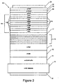
- Figure 2 illustrates further embodiments of the present invention incorporating a multi-quantum well active region.
- the embodiments of the present invention illustrated in Figure 2 include a layered semiconductor structure 100 comprising gallium nitride-based semiconductor layers grown on a substrate 10.
- the substrate 10 may be SiC, sapphire or bulk gallium nitride.
- LEDs may include a conductive buffer layer 11, a first silicon-doped GaN layer 12, a second silicon doped GaN layer 14, a superlattice structure 16 comprising alternating layers of silicon-doped GaN and/or InGaN, an active region 125 comprising a multi-quantum well structure, an undoped GaN or AlGaN layer 22, an AIGaN layer 30 doped with a p-type impurity, and a GaN contact layer 32, also doped with a p-type impurity.
- the LEDs may further include an n-type ohmic contact 23 on the substrate 10 and a p-type ohmic contact 24 on the contact layer 32. In embodiments of the present invention where the substrate 10 is sapphire, the n-type ohmic contact 23 would be provided on n-type GaN layer 12 and/or n-type GaN layer 14.
- buffer layer 11 is preferably n-type AlGaN.
- GaN layer 12 is preferably between about 500 and 4000 nm thick inclusive and is most preferably about 1500 nm thick.
- GaN layer 12 may be doped with silicon at a level of about 5x10 17 to 5x10 18 cm -3 .
- GaN layer 14 is preferably between about 1 and 50 nm (10 and 500 ⁇ ) thick inclusive, and is most preferably about 8 nm (80 ⁇ ) thick.
- GaN layer 14 may be doped with silicon at a level of less than about 5x10 19 cm -3 .
- the superlattice structure 16 may also be provided as described above with reference to Figure 1 .
- the active region 125 comprises a multi-quantum well structure that includes multiple InGaN quantum well layers 120 separated by barrier layers 118.
- the barrier layers 118 comprise In X Ga 1-X N where 0 ⁇ X ⁇ 1.
- the indium composition of the barrier layers 118 is less than that of the quantum well layers 120, so that the barrier layers 118 have a higher bandgap than quantum well layers 120.
- the barrier layers 118 and quantum well layers 120 may be undoped ( i . e . not intentionally doped with an impurity atom such as silicon or magnesium). However, it may be desirable to dope the barrier layers 118 with Si at a level of less than 5x10 19 cm -3 , particularly if ultraviolet emission is desired.
- the barrier layers 118 comprise Al X In Y Ga 1-X-Y N where 0 ⁇ X ⁇ 1, 0 ⁇ Y ⁇ 1 and X+Y ⁇ 1.
- the barrier layers 118 may be lattice-matched to the quantum well layers 120, thereby providing improved crystalline quality in the quantum well layers 120, which increases the luminescent efficiency of the device.
- an active region 225 comprises a periodically repeating structure 221 comprising a well support layer 218a having high crystal quality, a quantum well layer 220 and a cap layer 218b that serves as a protective cap layer for the quantum well layer 220.
- the cap layer 218b and the well support layer 218a together form the barrier layer between adjacent quantum wells 220.
- the high quality well support layer 218a is grown at a higher temperature than that used to grow the InGaN quantum well layer 220.
- the well support layer 218a is grown at a slower growth rate than the cap layer 218b.
- lower growth rates may be used during the lower temperature growth process and higher growth rates utilized during the higher temperature growth process.
- the well support layer 218a may be grown at a growth temperature of between 700 and 900 °C. Then, the temperature of the growth chamber is lowered by up to 200 °C to permit growth of the high-quality InGaN quantum well layer 220. Then, while the temperature is kept at the lower InGaN growth temperature, the cap layer 218b is grown. In that manner, a multi-quantum well region comprising high quality InGaN layers may be fabricated.
- the active regions 125 and 225 of Figures 2 and 3 are preferably grown in a nitrogen atmosphere, which may provide increased InGaN crystal quality.
- the barrier layers 118, the well support layers 218a and/or the cap layers 218b may be between about 50 - 400 ⁇ thick inclusive.
- the combined thickness of corresponding ones of the well support layers 218a and the cap layers 218b may be up to 40 nm (400 ⁇ ) thick inclusive.
- the barrier layers 118 the well support layers 218a and/or the cap layers 218b are greater than 9nm (90 ⁇ ) thick and most preferably are about 22.5nm (225 ⁇ ) thick.
- the cap layers 218b are preferably as thin as possible while still reducing the desorption of Indium from or the degradation of the quantum well layers 220.
- the quantum well layers 120 and 220 may be between about 1-5nm (10 - 50 ⁇ ) thick inclusive.
- the quantum well layers 120 and 220 are greater than 2nm (20 ⁇ ) thick and most preferably are about 2.5 nm (25 ⁇ ) thick.
- the thickness and percentage of indium in the quantum well layers 120 and 220 may be varied to produce light having a desired wavelength. Typically, the percentage of indium in quantum well layers 120 and 220 is about 25-30%, however, depending on the desired wavelength, the percentage of indium has been varied from about 5% to about 50%.
- the bandgap of the superlattice structure 16 exceeds the bandgap of the quantum well layers 120. This may be achieved by by adjusting the average percentage of indium in the superlattice 16.
- the thickness (or period) of the superlattice layers and the average Indium percentage of the layers should be chosen such that the bandgap of the superlattice structure 16 is greater than the bandgap of the quantum wells 120.
- the bandgap of the superlattice structure 16 may be from about 2.95 eV to about 3.35 eV. In a preferred embodiment, the bandgap of the superlattice structure 16 is about 3.15 eV.
- the LED structure illustrated in Figure 2 includes a spacer layer 17 disposed between the superlattice 16 and the active region 125.
- the spacer layer 17 preferably comprises undoped GaN.
- the presence of the optional spacer layer 17 between the doped superlattice 16 and active region 125 may deter silicon impurities from becoming incorporated into the active region 125. This, in turn, may improve the material quality of the active region 125 that provides more consistent device performance and better uniformity.
- a spacer layer may also be provided in the LED structure illustrated in Figure 1 between the superlattice 16 and the active region 18.
- the layer 22 may be provided on the active region 125 and is preferably undoped GaN or AlGaN between about 0 and 12 nm (120 ⁇ ) thick inclusive.
- the layer 22 is preferably about 3.5 nm (35 ⁇ ) thick. If the layer 22 comprises AlGaN, the aluminum percentage in such layer is preferably about 10-30% and most preferably about 24%.
- the level of aluminum in the layer 22 may also be graded in a stepwise or continuously decreasing fashion.
- the layer 22 may be grown at a higher temperature than the growth temperatures in the active region 125 in order to improve the crystal quality of the layer 22. Additional layers of undoped GaN or AlGaN may be included in the vicinity of layer 22.
- the LED illustrated in Figure 2 may include an additional layer of undoped AlGaN about 0.6-0.9nm (6-9 ⁇ ) thick between the active regions 125 and the layer 22.
- An AlGaN layer 30 doped with a p-type impurity such as magnesium is provided on layer 22.
- the AlGaN layer 30 may be between about 0 and 30nm (300 ⁇ ) thick inclusive and is preferably about 13nm (130 ⁇ ) thick.
- a contact layer 32 of p-type GaN is provided on the layer 30 and is preferably about 180nm (1800 ⁇ ) thick.
- Ohmic contacts 24 and 25 are provided on the p-GaN contact layer 32 and the substrate 10, respectively.
- Ohmic contacts 24 and 25 are provided on the p-GaN contact layer 32 and the substrate 10, respectively.
- embodiments of the present invention have been described with reference to gallium nitride based devices, the teachings and benefits of the present invention may also be provided in other Group III nitrides.
- embodiments of the present invention provide Group III nitride based superlattice structures, quantum well structures and/or Group III nitride based light emitting diodes having superlattices and/or quantum wells.
Abstract
Description
- This invention relates to microelectronic devices and fabrication methods therefor, and more particularly to structures which may be utilized in Group III nitride semiconductor devices, such as light emitting diodes (LEDs).
- Light emitting diodes are widely used in consumer and commercial applications. As is well known to those having skill in the art, a light emitting diode generally includes a diode region on a microelectronic substrate. The microelectronic substrate may comprise, for example, gallium arsenide, gallium phosphide, alloys thereof, silicon carbide and/or sapphire. Continued developments in LEDs have resulted in highly efficient and mechanically robust light sources that can cover the visible spectrum and beyond. These attributes, coupled with the potentially long service life of solid state devices, may enable a variety of new display applications, and may place LEDs in a position to compete with the well entrenched incandescent lamp.
-
US-A-6,153,894 discloses technology for obtaining a shortwave light-emitting device made of a group-III nitride semiconductor crystal, and in particular, technology for fabricating a light-emitting layer which results in a high brightness luminescent light and in emission of a longer wavelength of light. The device comprises a light-emitting layer on a superlattice structure as a base layer, resulting in an improved crystallinity of the light-emitting layer. Furthermore, an abruptness of a crystal composition at the interface of the light-emitting layer and the upper junction layer is achieved, thus forming a bending portion of a band structure expedient for allowing the emitting-layer to emit a light with a long wavelength. -
US 6,153 ,894 discloses in particular a method of manufacturing a Group-III nitride-based semiconductor device having a multiple quantum well structure, comprising the steps of repeatedly forming a GaN barrier layer with a thickness of 20 nm and an InGaN quantum well layer with a thickness of 10 nm. -
WO 0076004 -
JP11040850 - One difficultly in fabricating Group III nitride based LEDs, such as gallium nitride based LEDs, has been with the fabrication of high quality gallium nitride. Typically, gallium nitride LEDs have been fabricated on sapphire or silicon carbide substrates. Such substrates may result in mismatches between the crystal lattice of the substrate and the gallium nitride. Various techniques have been employed to overcome potential problems with the growth of gallium nitride on sapphire and/or silicon carbide. For example, aluminum nitride (AIN) may be utilized as a buffer between a silicon carbide substrate and a Group III active layer, particularly a gallium nitride active layer. Typically, however, aluminum nitride is insulating rather than conductive. Thus, structures with aluminum nitride buffer layers typically require shorting contacts that bypass the aluminum nitride buffer to electrically link the conductive silicon carbide substrate to the Group III nitride active layer.
- Alternatively, conductive buffer layer materials such as gallium nitride (GaN), aluminum gallium nitride (AlGaN), or combinations of gallium nitride and aluminum gallium nitride may allow for elimination of the shorting contacts typically utilized with AIN buffer layers. Typically, eliminating the shorting contact reduces the epitaxial layer thickness, decreases the number of fabrication steps required to produce devices, reduces the overall chip size, and/or increases the device efficiency. Accordingly, Group III nitride devices may be produced at lower cost with a higher performance. Nevertheless, although these conductive buffer materials offer these advantages, their crystal lattice match with silicon carbide is less satisfactory than is that of aluminum nitride.
- The above described difficulties in providing high quality gallium nitride may result in reduced efficiency the device. Attempts to improve the output of Group III nitride based devices have included differing configurations of the active regions of the devices. Such attempts have, for example, included the use of single and/or double heterostructure active regions. Similarly, quantum well devices with one or more Group III nitride quantum wells have also been described. While such attempts have improved the efficiency of Group III based devices, further improvements may still be achieved.
- The present invention provides a Group III nitride-based semiconductor device having a multiple quantum well structure (18, 225) consisting of a periodically repeating quantum well structure (221) comprising:
- a Group III nitride-based well support layer (218a);
- a Group III nitride-based quantum well layer (220); and
- a Group III nitride-based cap layer (218b);
- Embodiments of the present invention provide a light emitting diode having a Group III nitride based superlattice and a Group III nitride based active region on the superlattice. The active region has the multiple quantum well structure.
- In further embodiments of the present invention, the light emitting diode may include up to 10 repetitions of the quantum well structure.
- In preferred embodiments of the present invention, the superlattice includes a gallium nitride based superlattice having at least two periods of alternating layers of InxGa1-xN and InyGa1-yN, where 0≤X<1 and 0≤Y<1 and X is not equal to Y. The first Group III nitride based barrier layer provides a well support layer comprising a Group III nitride and the second Group III nitride based barrier layer provides a cap layer comprising a Group III nitride on the quantum well layer.
- In still further embodiments of the present invention, the well support layer comprises a gallium nitride based layer, the quantum well layer comprises an indium gallium nitride layer and the barrier layer comprises a gallium nitride based layer. In such embodiments, the well support layer and the cap layer may be provided by layers of InxGa1-xN where 0≤X. Furthermore, the indium composition of the well support layer and the cap layer
- In still further embodiments of the present invention, the well support layer comprises a gallium nitride based layer, the quantum well layer comprises an indium gallium nitride layer and the barrier layer comprises a gallium nitride based layer. In such embodiments, the well support layer and the cap layer may be provided by layers of InxGa1-xN where 0≤X<1. Furthermore, the indium composition of the well support layer and the cap layer may be less than the indium composition of the quantum well layer.
- The well support layer and the cap layer may also be provided by a layer of AlxInyGa1-x-yN where 0<X<1, 0≤Y<1 and X+Y≤1. Furthermore, the well support layer and the cap layer may be undoped. Alternatively, the well support layer and the cap layer may have an n-type doping level of less than about 5x1019cm-3. The cap layer and the well support layer may also have a higher bandgap than the quantum well layer. The combined thickness of the well support layer and the cap layer may be up to 40nm (400 Å). The thickness of the well support layer may be greater than a thickness of the cap layer. The quantum well layer may have a thickness of from 1 to 5 nm (10 to 50 Å). For example, the quantum well layer may have a thickness of about 2 nm (20 Å). Furthermore, the percentage of indium in the quantum well layer may be from 15% to 40%.
- In additional embodiments of the present invention, a Group III nitride based spacer layer is provided between the well support layer and the superlattice. The spacer layer may be undoped GaN.
- In other embodiments of the present invention, the bandgap of the quantum well is less than the bandgap of the superlattice.
- In additional embodiments of the present invention, the gallium nitride based superlattice comprises from 5 to 50 periods. The alternating layers of InxGa1-xN and InyGa1-yN may have a combined thickness of from 1 to 14 nm (10 to 140 Å).
- In particular embodiments of the present invention, X = 0 for layers of InxGa1-xN of the superlattice. In such embodiments, the InGaN layers may have a thickness of from 0.5 to 4 nm (5 to 40 Å) and the GaN layers may have a thickness of from 0.5 to 10 nm (5 to 100 Å).
- In further embodiments of the present invention, the gallium nitride based superlattice is doped with an n-type impurity to a level of from 1x1017cm-3 to 5x1019cm-3. The doping level of the gallium nitride based superlattice may be an actual doping level of layers of the alternating layers. The doping level may also be an average doping level of layers of the alternating layers. Thus, for example, the light emitting diode may include doped Group III nitride layers adjacent the superlattice where the doped Group III nitride layers are doped with an n-type impurity to provide an average doping of the doped Group III nitride layers and the superlattice of from 1x1017cm-3 to 5x1019cm-3. The bandgap of the superlattice may be from 2.95 eV to 3.35 eV and, in certain embodiments, may be about 3.15 eV.
- In other embodiments of the present invention, a Group III nitride based semiconductor device having an active region comprising a multiple quantum well structure according to claim 1 is provided. The quantum well structure includes a well support layer comprising a Group III nitride, a quantum well layer comprising a Group III nitride on the well support layer and a cap layer comprising a Group III nitride on the quantum well layer.
- The cap layer has a lower crystal quality than the well support layer. The well support layer may be provided by a gallium nitride based layer, the quantum well layer may be provided by an indium gallium nitride layer and the barrier layer may be provided by a gallium nitride based layer. In such embodiments, the well support layer and the cap layer may be provided by layers of InXGa1-XN where 0≤X<1. Furthermore, the indium composition of the well support layer and the cap layer may be less the indium composition of the quantum well layer. Similarly, the well support layer and the cap layer may be provided by layers of AlXInYGa1-X-YN where 0<X<1, 0≤Y<1 and X+Y≤1.
- Furthermore, the well support layer and the cap layer may be undoped. Alternatively, the well support layer and the cap layer may have a doping level of less than about 5x1019 cm-3.
- In further embodiments of the present invention, the cap layer and the well support layer have a higher bandgap than the quantum well layer. The combined thickness of the well support layer and the cap layer may be up to 40 nm (400 Å,), typically about 22.5 nm (225 Å.). The thickness of the well support layer may be greater than the thickness of the cap layer.
- In additional embodiments of the present invention, the quantum well layer has a thickness of from about 1 to 5 nm (10 to about 50 Å.). For example, the quantum well layer may have a thickness of about 2.5 nm (25 Å.). Furthermore, the percentage of indium in the quantum well layer may from about 5% to about 50%.
- In further embodiments of the Group III nitride based semiconductor device according to the present invention, a superlattice is provided and the well support layer is on the superlattice. The superlattice may have a bandgap of about 3.15 eV. Furthermore, a Group III nitride based spacer layer may be provided between the well support layer and the superlattice. The spacer layer may be undoped GaN. Also, the bandgap of the at least one quantum well may be less than the bandgap of the superlattice.
- According to the present invention, a second well support layer comprising a Group III nitride is provided on the cap layer. A second quantum well layer comprising a Group III nitride is provided on the second well support layer; and a second cap layer comprising a Group III nitride is provided on the second quantum well layer.
- In particular embodiments of the present invention, the Group III nitride based semiconductor device includes up to 10 repetitions of the quantum well structures.
- Embodiments of the present invention further provide a Group III nitride based semiconductor device that includes a gallium nitride based superlattice having at least two periods of alternating layers of InXGa1-XN and InYGa1-YN, where 0 ≤ X < 1 and 0 ≤ Y < 1 and X is not equal to Y.
- In further embodiments of the present invention, the gallium nitride based superlattice includes from 5 to 50 periods. For example, the gallium nitride based superlattice may include 25 periods. Similarly, the gallium nitride based superlattice may include 10 periods.
- In additional embodiments of the present invention, the gallium nitride based superlattice comprises from 5 to 50 periods. The alternating layers of InXGa1-XN and InYGa1-YN may have a combined thickness of from 10 to 140 Å.
- In particular embodiments of the present invention, X = 0 for layers of InXGa1-X N of the superlattice. In such embodiments, the InGaN layers may have a thickness of from 0.5 to 4 nm (5 to 40 Å) and the GaN layers may have a thickness of from 0.5 to 10 nm (5 to 100 Å). In still further embodiments of the present invention, the gallium nitride based superlattice is doped with an n-type impurity to a level of from 1x1017 cm-3 to 5x1019cm-3. The doping level of the gallium nitride based superlattice may be an actual doping level of layers of the alternating layers or may be an average doping level of layers of the alternating layers.
- In certain embodiments of the present invention, doped Group III nitride layers are provided adjacent the superlattice. The doped Group III nitride layers are doped with an n-type impurity to provide an average doping of the doped Group III nitride layers and the superlattice of from 1x1017 cm-3 to 5x1019cm-3.
- In additional embodiments ot the present invention, a bandgap of the superlattice is about 3.15 eV.
- In embodiments of the present invention where the Group III nitride based semiconductor device comprises a light emitting diode, the light emitting diode includes a Group III nitride based active region on the superlattice. Additionally, a Group III nitride based spacer layer may also be provided between the active region and the superlattice. Such a spacer layer may be undoped GaN.
- In certain embodiments of the present invention, a bandgap of the quantum well may be less than a bandgap of the superlattice.
- Additional embodiments of the present invention provide a method of fabricating a Group III nitride based semiconductor device having an active region comprising a multiple quantum well structure according to claim 21. Each repetition of the quantum well structure is fabricated by forming a well support layer comprising a Group III nitride, forming a quantum well layer comprising a Group III nitride on the quantum well support layer and forming a cap layer comprising a Group III nitride on the quantum well layer.
- According to the present invention, forming a well support layer comprising a Group III nitride is provided by forming the well support layer at a first temperature. Forming a quantum well layer is provided by forming the quantum well layer at a second temperature which is less than the first temperature. Forming a cap layer is provided by forming the cap layer at a third temperature which is less than the first temperature. In certain embodiments of the present invention, the third temperature is substantially the same as the second temperature.
- In further embodiments of the present invention, the well support layer comprises a gallium nitride based layer, the quantum well layer comprises an indium gallium nitride layer and the cap layer comprises a gallium nitride based layer. In such embodiments, the first temperature may be from 700 to 900°C. Furthermore, the second temperature may be up to 200°C less than the first temperature. The indium gallium nitride layer may be formed in a nitrogen atmosphere or other atmosphere.
- Preferably, forming a well support layer and forming a cap layer are provided by forming a cap layer of InXGa1-XN, where 0≤X<1 and forming a well support layer of InXGa1-XN, where 0≤X<1. Also, the indium composition of the well support layer and the cap layer may be less an indium composition of the quantum well layer.
- In additional embodiments of the present invention, forming a well support layer and forming a cap layer are provided by forming a cap layer of AlXInYGa1-X-YN, where 0<X<1, 0≤Y<1 and X+Y≤1 and forming a well support layer of AlXInYGa1-X-Y N, where 0<X<1, 0≤Y<1 and X+Y≤1.
- Further embodiments of the present invention include forming a superlattice, where the well support layer is on the superlattice. Additional embodiments of the present invention include, forming a Group III nitride based spacer layer between the well support layer and the superlattice. The spacer layer may be undoped GaN. The present invention includes forming a second well support layer comprising a Group III nitride on the cap layer, forming a second quantum well layer comprising a Group III nitride on the second well support layer and forming a second cap layer comprising a Group III nitride on the second quantum well layer. The second well support layer is formed at the first temperature, the second quantum well layer is formed at the second temperature which is less than the first temperature and the second cap layer is formed at the third temperature which is less than the first temperature.
- Other features of the present invention will be more readily understood from the following detailed description of specific embodiments thereof when read in conjunction with the accompanying drawings, in which:
-
Figure 1 is a schematic illustration of a Group III nitride light emitting diode incorporating embodiments of the present invention; -
Figure 2 is a schematic illustration of a Group III nitride light emitting diode incorporating further embodiments of the present invention; and -
Figure 3 is a schematic illustration of a quantum well structure and a multi-quantum well structure according to additional embodiments of the present invention. - The present invention now will be described more fully hereinafter with reference to the accompanying drawings, in which preferred embodiments of the invention are shown. This invention may, however, be embodied in many different forms and should not be construed as limited to the embodiments set forth herein. Rather, these embodiments are provided so that this disclosure will be thorough and complete, and will fully convey the scope of the invention to those skilled in the art. In the drawings, the thickness of layers and regions are exaggerated for clarity. Like numbers refer to like elements throughout. It will be understood that when an element such as a layer, region or substrate is referred to as being "on" or extending "onto" another element, it can be directly on or extend directly onto the other element or intervening elements may also be present. In contrast, when an element is referred to as being "directly on" or extending "directly onto" another element, there are no intervening elements present. Moreover, each embodiment described and illustrated herein includes its complementary conductivity type embodiment as well.
- Embodiments of the present invention will be described with reference to
Figure 1 that illustrates a light emitting diode (LED)structure 40. TheLED structure 40 ofFigure 1 includes asubstrate 10, which is preferably 4H or 6H n-type silicon carbide.Substrate 10 may also comprise sapphire, bulk gallium nitride or another suitable substrate. Also included in theLED structure 40 ofFigure 1 is a layered semiconductor structure comprising gallium nitride-based semiconductor layers onsubstrate 10. Namely, theLED structure 40 illustrated includes the following layers: aconductive buffer layer 11, a first silicon-dopedGaN layer 12, a second silicon dopedGaN layer 14, asuperlattice structure 16 comprising alternating layers of silicon-doped GaN and/or InGaN, anactive region 18, provided by a multi-quantum well structure, an undoped GaN and/orAlGaN layer 22, anAlGaN layer 30 doped with a p-type impurity, and aGaN contact layer 32, also doped with a p-type impurity. The structure further includes an n-type ohmic contact 23 on thesubstrate 10 and a p-type ohmic contact 24 on thecontact layer 32. -
Buffer layer 11 is preferably n-type AlGaN. Examples of buffer layers between silicon carbide and group III-nitride materials are provided inU.S. Patents 5,393,993 and5,523,589 , and6,459,100 entitled "Vertical Geometry InGaN Light Emitting Diode" assigned to the assignee of the present invention. - Similarly, embodiments of the present invention may also include structures such as those described in United States Patent No.
6,201,262 entitled "Group III Nitride Photonic Devices on Silicon Carbide Substrates With Conductive Buffer Interlay Structure,". -
GaN layer 12 is preferably between about 500 and 4000 nm thick inclusive and is most preferably about 1500 nm thick.GaN layer 12 may be doped with silicon at a level of about 5x10¹⁷ to 5x1018 cm-3.GaN layer 14 is preferably between about 1 and 50 nm (10 and 500 Å) thick inclusive, and is most preferably about 8 nm (80 Å) thick.GaN layer 14 may be doped with silicon at a level of less than about 5x1019 cm-3. - As illustrated in
Figure 1 , asuperlattice structure 16 according to embodiments of the present invention includes alternating layers of InXGa1-XN and InYGa1-YN, wherein X is between 0 and 1 inclusive and X is not equal to Y. Preferably, X=0 and the thickness of each of the alternating layers of InGaN is about 0.5-4 nm (5-40 Å) thick inclusive, and the thickness of each of the alternating layers of GaN is about 0.5-10 nm (5-100 Å) thick inclusive. In certain embodiments, the GaN layers are about 3 nm (30 Å) thick and the InGaN layers are about 1.5 nm (15 Å) thick. Thesuperlattice structure 16 may include from about 5 to about 50 periods (where one period equals one repetition each of the InXGa1-XN and InYGa1-YN layers that comprise the superlattice). In one embodiment, thesuperlattice structure 16 comprises 25 periods. In another embodiment, thesuperlattice structure 16 comprises 10 periods. The number of periods, however, may be decreased by, for example, increasing the thickness of the respective layers. Thus, for example, doubling the thickness of the layers may be utilized with half the number of periods. Alternatively, the number and thickness of the periods may be independent of one another. - Preferably, the
superlattice 16 is doped with an n-type impurity such as silicon at a level of from about 1x1017 cm-3 to about 5x1019 cm-3. Such a doping level may be actual doping or average doping of the layers of thesuperlattice 16. If such doping level is an average doping level, then it may be beneficial to provide doped layers adjacent thesuperlattice structure 16 that provide the desired average doping which the doping of the adjacent layers is averaged over the adjacent layers and thesuperlattice structure 16. By providing thesuperlattice 16 betweensubstrate 10 andactive region 18, a better surface may be provided on which to grow InGaN-basedactive region 18. While not wishing to be bound by any theory of operation, the inventors believe that strain effects in thesuperlattice structure 16 provide a growth surface that is conductive to the growth of a high-quality InGaN-containing active region. Further, the superlattice is known to influence the operating voltage of the device. Appropriate choice of superlattice thickness and composition parameters can reduce operating voltage and increase optical efficiency. - The
superlattice structure 16 may be grown in an atmosphere of nitrogen or other gas, which enables growth of higher-quality InGaN layers in the structure. By growing a silicon-doped InGaN/GaN superlattice on a silicon-doped GaN layer in a nitrogen atmosphere, a structure having improved crystallinity and conductivity with optimized strain may be realized. - In particular embodiments of the present invention, the
active region 18 comprises a multi-quantum well structure that includes multiple InGaN quantum well layers separated by barrier layers (not shown inFigure 1 ). -
Layer 22 is provided onactive region 18 and is preferably undoped GaN or AlGaN between about 0 and 12 nm (120 Å) thick inclusive. As used herein, undoped refers to a not intentionally doped.Layer 22 is preferably about 3.5 nm (35 Å) thick. Iflayer 22 comprises AlGaN, the aluminum percentage in such layer is preferably about 10-30% and most preferably about 24%. The level of aluminum inlayer 22 may also be graded in a stepwise or continuously decreasing fashion.Layer 22 may be grown at a higher temperature than the growth temperatures in quantum well region 25 in order to improve the crystal quality oflayer 22. Additional layers of undoped GaN or AlGaN may be included in the vicinity oflayer 22. For example, LED 1 may include an additional layer of undoped AlGaN about 6-9Å thick between theactive region 18 and thelayer 22. - An
AlGaN layer 30 doped with a p-type impurity such as magnesium is provided onlayer 22. TheAlGaN layer 30 may be between about 0 and 30 nm (300 Å) thick inclusive and is preferably about 13 nm (130 Å) thick. Acontact layer 32 of p-type GaN is provided on thelayer 30 and is preferably about 180 nm (1800 Å) thick.Ohmic contacts 24 and 25 are provided on the p-GaN contact layer 32 and thesubstrate 10, respectively. -
Figure 2 illustrates further embodiments of the present invention incorporating a multi-quantum well active region. The embodiments of the present invention illustrated inFigure 2 include alayered semiconductor structure 100 comprising gallium nitride-based semiconductor layers grown on asubstrate 10. As described above, thesubstrate 10 may be SiC, sapphire or bulk gallium nitride. As is illustrated inFigure 2 , LEDs according to particular embodiments of the present invention may include aconductive buffer layer 11, a first silicon-dopedGaN layer 12, a second silicon dopedGaN layer 14, asuperlattice structure 16 comprising alternating layers of silicon-doped GaN and/or InGaN, anactive region 125 comprising a multi-quantum well structure, an undoped GaN orAlGaN layer 22, anAIGaN layer 30 doped with a p-type impurity, and aGaN contact layer 32, also doped with a p-type impurity. The LEDs may further include an n-type ohmic contact 23 on thesubstrate 10 and a p-type ohmic contact 24 on thecontact layer 32. In embodiments of the present invention where thesubstrate 10 is sapphire, the n-type ohmic contact 23 would be provided on n-type GaN layer 12 and/or n-type GaN layer 14. - As described above with reference to
Figure 1 ,buffer layer 11 is preferably n-type AlGaN. Similarly,GaN layer 12 is preferably between about 500 and 4000 nm thick inclusive and is most preferably about 1500 nm thick.GaN layer 12 may be doped with silicon at a level of about 5x10¹⁷ to 5x1018 cm-3.GaN layer 14 is preferably between about 1 and 50 nm (10 and 500 Å) thick inclusive, and is most preferably about 8 nm (80 Å) thick.GaN layer 14 may be doped with silicon at a level of less than about 5x1019 cm-3. Thesuperlattice structure 16 may also be provided as described above with reference toFigure 1 . - The
active region 125 comprises a multi-quantum well structure that includes multiple InGaN quantum well layers 120 separated by barrier layers 118. The barrier layers 118 comprise InXGa1-XN where 0≤X<1. Preferably the indium composition of the barrier layers 118 is less than that of the quantum well layers 120, so that the barrier layers 118 have a higher bandgap than quantum well layers 120. The barrier layers 118 and quantum well layers 120 may be undoped (i.e. not intentionally doped with an impurity atom such as silicon or magnesium). However, it may be desirable to dope the barrier layers 118 with Si at a level of less than 5x1019 cm-3, particularly if ultraviolet emission is desired. - In further embodiments of the present invention, the barrier layers 118 comprise AlXInYGa1-X-YN where 0<X<1, 0≤Y<1 and X+Y ≤1. By including aluminum in the crystal of the barrier layers 118, the barrier layers 118 may be lattice-matched to the quantum well layers 120, thereby providing improved crystalline quality in the quantum well layers 120, which increases the luminescent efficiency of the device.
- Referring to
Figure 3 , embodiments of the present invention that provide a multi-quantum well structure of a gallium nitride based device are illustrated. The multi-quantum well structure illustrated inFigure 3 may provide the active region of the LEDs illustrated inFigure 1 and/orFigure 2 . As seen inFigure 3 , anactive region 225 comprises a periodically repeatingstructure 221 comprising awell support layer 218a having high crystal quality, aquantum well layer 220 and acap layer 218b that serves as a protective cap layer for thequantum well layer 220. When thestructure 221 is grown, thecap layer 218b and thewell support layer 218a together form the barrier layer between adjacentquantum wells 220. The high qualitywell support layer 218a is grown at a higher temperature than that used to grow the InGaNquantum well layer 220. In some embodiments of the present invention, thewell support layer 218a is grown at a slower growth rate than thecap layer 218b. In other embodiments, lower growth rates may be used during the lower temperature growth process and higher growth rates utilized during the higher temperature growth process. For example, in order to achieve a high quality surface for growing the InGaNquantum well layer 220, thewell support layer 218a may be grown at a growth temperature of between 700 and 900 °C. Then, the temperature of the growth chamber is lowered by up to 200 °C to permit growth of the high-quality InGaNquantum well layer 220. Then, while the temperature is kept at the lower InGaN growth temperature, thecap layer 218b is grown. In that manner, a multi-quantum well region comprising high quality InGaN layers may be fabricated. - The
active regions Figures 2 and3 are preferably grown in a nitrogen atmosphere, which may provide increased InGaN crystal quality. The barrier layers 118, thewell support layers 218a and/or the cap layers 218b may be between about 50 - 400 Å thick inclusive. The combined thickness of corresponding ones of thewell support layers 218a and the cap layers 218b may be up to 40 nm (400 Å) thick inclusive. Preferably, the barrier layers 118 thewell support layers 218a and/or the cap layers 218b are greater than 9nm (90 Å) thick and most preferably are about 22.5nm (225 Å) thick. Also, it is preferred that thewell support layers 218a be thicker than the cap layers 218b. Thus, the cap layers 218b are preferably as thin as possible while still reducing the desorption of Indium from or the degradation of the quantum well layers 220. The quantum well layers 120 and 220 may be between about 1-5nm (10 - 50 Å) thick inclusive. Preferably, the quantum well layers 120 and 220 are greater than 2nm (20 Å) thick and most preferably are about 2.5 nm (25 Å) thick. The thickness and percentage of indium in the quantum well layers 120 and 220 may be varied to produce light having a desired wavelength. Typically, the percentage of indium in quantum well layers 120 and 220 is about 25-30%, however, depending on the desired wavelength, the percentage of indium has been varied from about 5% to about 50%. - In preferred embodiments of the present invention, the bandgap of the
superlattice structure 16 exceeds the bandgap of the quantum well layers 120. This may be achieved by by adjusting the average percentage of indium in thesuperlattice 16. The thickness (or period) of the superlattice layers and the average Indium percentage of the layers should be chosen such that the bandgap of thesuperlattice structure 16 is greater than the bandgap of thequantum wells 120. By keeping the bandgap of thesuperlattice 16 higher than the bandgap of thequantum wells 120, unwanted absorption in the device may be minimized and luminescent emission may be maximized. The bandgap of thesuperlattice structure 16 may be from about 2.95 eV to about 3.35 eV. In a preferred embodiment, the bandgap of thesuperlattice structure 16 is about 3.15 eV. - In additional embodiments of the present invention, the LED structure illustrated in
Figure 2 includes aspacer layer 17 disposed between thesuperlattice 16 and theactive region 125. Thespacer layer 17 preferably comprises undoped GaN. The presence of theoptional spacer layer 17 between the dopedsuperlattice 16 andactive region 125 may deter silicon impurities from becoming incorporated into theactive region 125. This, in turn, may improve the material quality of theactive region 125 that provides more consistent device performance and better uniformity. Similarly, a spacer layer may also be provided in the LED structure illustrated inFigure 1 between thesuperlattice 16 and theactive region 18. - Returning to
Figure 2 , thelayer 22 may be provided on theactive region 125 and is preferably undoped GaN or AlGaN between about 0 and 12 nm (120 Å) thick inclusive. Thelayer 22 is preferably about 3.5 nm (35 Å) thick. If thelayer 22 comprises AlGaN, the aluminum percentage in such layer is preferably about 10-30% and most preferably about 24%. The level of aluminum in thelayer 22 may also be graded in a stepwise or continuously decreasing fashion. Thelayer 22 may be grown at a higher temperature than the growth temperatures in theactive region 125 in order to improve the crystal quality of thelayer 22. Additional layers of undoped GaN or AlGaN may be included in the vicinity oflayer 22. For example, the LED illustrated inFigure 2 may include an additional layer of undoped AlGaN about 0.6-0.9nm (6-9Å) thick between theactive regions 125 and thelayer 22. - An
AlGaN layer 30 doped with a p-type impurity such as magnesium is provided onlayer 22. TheAlGaN layer 30 may be between about 0 and 30nm (300 Å) thick inclusive and is preferably about 13nm (130 Å) thick. Acontact layer 32 of p-type GaN is provided on thelayer 30 and is preferably about 180nm (1800 Å) thick.Ohmic contacts 24 and 25 are provided on the p-GaN contact layer 32 and thesubstrate 10, respectively.Ohmic contacts 24 and 25 are provided on the p-GaN contact layer 32 and thesubstrate 10, respectively. - While embodiments of the present invention have been described with reference to gallium nitride based devices, the teachings and benefits of the present invention may also be provided in other Group III nitrides. Thus, embodiments of the present invention provide Group III nitride based superlattice structures, quantum well structures and/or Group III nitride based light emitting diodes having superlattices and/or quantum wells.
Claims (26)
- A Group III nitride-based semiconductor device having a multiple quantum well structure (18, 225) consisting of a periodically repeating quantum well structure (221) comprising:a Group III nitride-based well support layer (218a);a Group III nitride-based quantum well layer (220); anda Group III nitride-based cap layer (218b);wherein in each of said quantum well structures said quantum well layer (220) and said cap layer (218b) have a lower crystal quality than the well support layer (218a) and wherein said cap layer (218b) has a thickness of more than 9nm.
- A Group III nitride-based semiconductor device according to claim 1 wherein the well support layers (218a) are gallium nitride-based layers, the quantum well layers (220) are indium gallium nitride layers and the cap layers (218b) are gallium nitride based layers.
- A Group III nitride-based semiconductor device according to claim 2 wherein the percentage of indium in the quantum well layers is from 5 to 50%.
- A Group III nitride-based semiconductor device according to claim 2 or claim 3, wherein the well support layers and the cap layers are InxGa1-xN layers where 0≤X<1.
- A Group III nitride-based semiconductor device according to claim 2 or claim 3 wherein the well support layers and the cap layers are AℓxInyGa1-x-yN where 0<X<1, 0≤Y<1 and X+Y≤1.
- A group III nitride-based semiconductor device according to claim 6 wherein X≤Y+0.05.
- A Group III nitride-based semiconductor device according to any one of claims 2 to 6 wherein the well support layers and the cap layers are undoped.
- A Group III nitride-based semiconductor device according to any one of claims 2 to 6 wherein the well support layers and the cap layers have a doping level of less than 5x1019cm-3.
- A Group III nitride-based semiconductor device according to any preceding claim wherein the cap layers and the well support layers have a greater bandgap than the quantum well layers.
- A Group III nitride-based semiconductor device according to any preceding claim wherein in each of said quantum well structures the combined thickness of the well support layer and the cap layer is 40nm.
- A Group III nitride-based semiconductor device according to any preceding claim wherein in each of said quantum well structures the thickness of the well support layer is greater than the thickness of the cap layer.
- A Group III nitride-based semiconductor device according to any one of claims 1 to 10 wherein the quantum well layers have a thickness of from 1 to 5nm.
- A Group III nitride-based semiconductor device according to claim 12 wherein the quantum well layers have a thickness of 2.5nm.
- A Group III nitride-based semiconductor device according to any preceding claim further comprising a superlattice and wherein the first well support layer is on the superlattice structure.
- A Group III nitride-based semiconductor device according to claim 14 wherein the superlattice structure has a bandgap of 2.95 to 3.35 eV.
- A Group III nitride-based semiconductor device according to claim 15 wherein the superlattice structure has a bandgap of 3.15 eV.
- A Group III nitride-based semiconductor device according to any one of claims 14 to 16 further comprising a Group III nitride-based spacer layer between the first well support layer and the superlattice structure.
- A Group III nitride-based semiconductor device according to claim 17 wherein the spacer layer is undoped GaN.
- A Group III nitride-based semiconductor device according to any one of claims 15 to 18 wherein the bandgap of each of said quantum wells is less than the bandgap of the superlattice structure.
- A Group III nitride-based semiconductor device according to any preceding claim having from 2 to 10 repetitions of the quantum well structure.
- A method of fabricating a Group III nitride-based semiconductor device according to any preceding claim comprising the steps of forming a multiple quantum well structure (18, 25) consisting of a periodically repeating structure (221) by:forming a Group III nitride-based well support layer (218a) at a first temperature of 700 to 900°C;forming a Group III nitride-based quantum well layer (220) on the quantum well support layer at a second temperature that is less than said first temperature; andforming a Group III nitride-based cap layer (218b) on said quantum well layer at a third temperature that is less than said first temperature;wherein in each of said quantum well structures said cap layer (218b) has a thickness of more than 9nm.
- A method according to claim 21 wherein said second temperature is up to 200°C less than said first temperature.
- A method according to claim 21 or claim 22 wherein the well support layers are gallium nitride based layers, the quantum well layers are indium gallium nitride layers and the cap layer is a gallium nitride based layer and wherein the indium gallium nitride layer is formed in a nitrogen atmosphere.
- A method according to any one of claims 21 to 23 further comprising the step of forming a superlattice structure, wherein the well support layer (218a) is formed on the superlattice structure.
- A method according to claim 24 further comprising the step of forming a Group III nitride-based spacer layer between the first well support layer and the superlattice structure.
- A method according to any one of claims 21 to 25 further comprising forming 2 to 10 repetitions of said quantum well structure.
Priority Applications (4)
| Application Number | Priority Date | Filing Date | Title |
|---|---|---|---|
| EP10180148.8A EP2259347B1 (en) | 2001-05-30 | 2002-05-23 | Group III nitride based light emitting diodes with a quantum well and a superlattice |
| EP09157557.1A EP2075855B1 (en) | 2001-05-30 | 2002-05-23 | Group III nitride based light emitting diode with a superlattice structure |
| EP03078515A EP1401027B1 (en) | 2001-05-30 | 2002-05-23 | Group III nitride based light emitting diode with a superlattice structure |
| EP10169310.9A EP2237334B1 (en) | 2001-05-30 | 2002-05-23 | Group III nitride based light emitting diode |
Applications Claiming Priority (9)
| Application Number | Priority Date | Filing Date | Title |
|---|---|---|---|
| US29430801P | 2001-05-30 | 2001-05-30 | |
| US29444501P | 2001-05-30 | 2001-05-30 | |
| US29437801P | 2001-05-30 | 2001-05-30 | |
| US294378P | 2001-05-30 | ||
| US294308P | 2001-05-30 | ||
| US294445P | 2001-05-30 | ||
| US140796 | 2002-05-07 | ||
| US10/140,796 US6958497B2 (en) | 2001-05-30 | 2002-05-07 | Group III nitride based light emitting diode structures with a quantum well and superlattice, group III nitride based quantum well structures and group III nitride based superlattice structures |
| PCT/US2002/016407 WO2002097904A2 (en) | 2001-05-30 | 2002-05-23 | Group iii nitride based light emitting diode structures with a quantum well and superlattice |
Related Child Applications (4)
| Application Number | Title | Priority Date | Filing Date |
|---|---|---|---|
| EP10169310.9A Division EP2237334B1 (en) | 2001-05-30 | 2002-05-23 | Group III nitride based light emitting diode |
| EP10180148.8A Division EP2259347B1 (en) | 2001-05-30 | 2002-05-23 | Group III nitride based light emitting diodes with a quantum well and a superlattice |
| EP09157557.1A Division EP2075855B1 (en) | 2001-05-30 | 2002-05-23 | Group III nitride based light emitting diode with a superlattice structure |
| EP03078515A Division EP1401027B1 (en) | 2001-05-30 | 2002-05-23 | Group III nitride based light emitting diode with a superlattice structure |
Publications (2)
| Publication Number | Publication Date |
|---|---|
| EP1390990A2 EP1390990A2 (en) | 2004-02-25 |
| EP1390990B1 true EP1390990B1 (en) | 2008-10-22 |
Family
ID=27495441
Family Applications (4)
| Application Number | Title | Priority Date | Filing Date |
|---|---|---|---|
| EP10169310.9A Expired - Lifetime EP2237334B1 (en) | 2001-05-30 | 2002-05-23 | Group III nitride based light emitting diode |
| EP02726917A Expired - Lifetime EP1390990B1 (en) | 2001-05-30 | 2002-05-23 | Group iii nitride based semiconductor device with a multiple quantum well structure |
| EP09157557.1A Expired - Lifetime EP2075855B1 (en) | 2001-05-30 | 2002-05-23 | Group III nitride based light emitting diode with a superlattice structure |
| EP10180148.8A Expired - Lifetime EP2259347B1 (en) | 2001-05-30 | 2002-05-23 | Group III nitride based light emitting diodes with a quantum well and a superlattice |
Family Applications Before (1)
| Application Number | Title | Priority Date | Filing Date |
|---|---|---|---|
| EP10169310.9A Expired - Lifetime EP2237334B1 (en) | 2001-05-30 | 2002-05-23 | Group III nitride based light emitting diode |
Family Applications After (2)
| Application Number | Title | Priority Date | Filing Date |
|---|---|---|---|
| EP09157557.1A Expired - Lifetime EP2075855B1 (en) | 2001-05-30 | 2002-05-23 | Group III nitride based light emitting diode with a superlattice structure |
| EP10180148.8A Expired - Lifetime EP2259347B1 (en) | 2001-05-30 | 2002-05-23 | Group III nitride based light emitting diodes with a quantum well and a superlattice |
Country Status (12)
| Country | Link |
|---|---|
| US (7) | US6958497B2 (en) |
| EP (4) | EP2237334B1 (en) |
| JP (5) | JP2005507155A (en) |
| KR (4) | KR101032847B1 (en) |
| CN (1) | CN100350637C (en) |
| AT (2) | ATE412253T1 (en) |
| AU (1) | AU2002257318A1 (en) |
| CA (1) | CA2441310A1 (en) |
| DE (2) | DE60229514D1 (en) |
| MY (1) | MY137396A (en) |
| TW (1) | TW544952B (en) |
| WO (1) | WO2002097904A2 (en) |
Families Citing this family (388)
| Publication number | Priority date | Publication date | Assignee | Title |
|---|---|---|---|---|
| US6800876B2 (en) | 2001-01-16 | 2004-10-05 | Cree, Inc. | Group III nitride LED with undoped cladding layer (5000.137) |
| US6794684B2 (en) | 2001-02-01 | 2004-09-21 | Cree, Inc. | Reflective ohmic contacts for silicon carbide including a layer consisting essentially of nickel, methods of fabricating same, and light emitting devices including the same |
| US6791119B2 (en) * | 2001-02-01 | 2004-09-14 | Cree, Inc. | Light emitting diodes including modifications for light extraction |
| US7692182B2 (en) * | 2001-05-30 | 2010-04-06 | Cree, Inc. | Group III nitride based quantum well light emitting device structures with an indium containing capping structure |
| US6958497B2 (en) * | 2001-05-30 | 2005-10-25 | Cree, Inc. | Group III nitride based light emitting diode structures with a quantum well and superlattice, group III nitride based quantum well structures and group III nitride based superlattice structures |
| TW546855B (en) * | 2001-06-07 | 2003-08-11 | Sumitomo Chemical Co | Group 3-5 compound semiconductor and light emitting diode |
| JP2004531894A (en) | 2001-06-15 | 2004-10-14 | クリー インコーポレイテッド | UV light emitting diode |
| US7211833B2 (en) | 2001-07-23 | 2007-05-01 | Cree, Inc. | Light emitting diodes including barrier layers/sublayers |
| US6740906B2 (en) * | 2001-07-23 | 2004-05-25 | Cree, Inc. | Light emitting diodes including modifications for submount bonding |
| US7858403B2 (en) | 2001-10-31 | 2010-12-28 | Cree, Inc. | Methods and systems for fabricating broad spectrum light emitting devices |
| US20030090103A1 (en) * | 2001-11-09 | 2003-05-15 | Thomas Becker | Direct mailing device |
| US6893442B2 (en) * | 2002-06-14 | 2005-05-17 | Ablatrics, Inc. | Vacuum coagulation probe for atrial fibrillation treatment |
| US7572257B2 (en) * | 2002-06-14 | 2009-08-11 | Ncontact Surgical, Inc. | Vacuum coagulation and dissection probes |
| US8235990B2 (en) | 2002-06-14 | 2012-08-07 | Ncontact Surgical, Inc. | Vacuum coagulation probes |
| US7063698B2 (en) * | 2002-06-14 | 2006-06-20 | Ncontact Surgical, Inc. | Vacuum coagulation probes |
| US9439714B2 (en) * | 2003-04-29 | 2016-09-13 | Atricure, Inc. | Vacuum coagulation probes |
| SG115549A1 (en) * | 2002-07-08 | 2005-10-28 | Sumitomo Chemical Co | Epitaxial substrate for compound semiconductor light emitting device, method for producing the same and light emitting device |
| GB2416920B (en) * | 2002-07-08 | 2006-09-27 | Sumitomo Chemical Co | Epitaxial substrate for compound semiconductor light - emitting device, method for producing the same and light - emitting device |
| KR100497890B1 (en) * | 2002-08-19 | 2005-06-29 | 엘지이노텍 주식회사 | Nitride semiconductor LED and fabrication method for thereof |
| WO2004027884A1 (en) * | 2002-09-19 | 2004-04-01 | Cree, Inc. | Phosphor-coated light emitting diodes including tapered sidewalls, and fabrication methods therefor |
| US7009199B2 (en) * | 2002-10-22 | 2006-03-07 | Cree, Inc. | Electronic devices having a header and antiparallel connected light emitting diodes for producing light from AC current |
| KR100906921B1 (en) * | 2002-12-09 | 2009-07-10 | 엘지이노텍 주식회사 | Manufacturing method of light emitting diode |
| KR101045160B1 (en) * | 2002-12-20 | 2011-06-30 | 크리 인코포레이티드 | Methods of forming semiconductor devices having self aligned semiconductor mesas and contact layers and related devices |
| US6885033B2 (en) * | 2003-03-10 | 2005-04-26 | Cree, Inc. | Light emitting devices for light conversion and methods and semiconductor chips for fabricating the same |
| US7531380B2 (en) * | 2003-04-30 | 2009-05-12 | Cree, Inc. | Methods of forming light-emitting devices having an active region with electrical contacts coupled to opposing surfaces thereof |
| US7087936B2 (en) * | 2003-04-30 | 2006-08-08 | Cree, Inc. | Methods of forming light-emitting devices having an antireflective layer that has a graded index of refraction |
| US7714345B2 (en) | 2003-04-30 | 2010-05-11 | Cree, Inc. | Light-emitting devices having coplanar electrical contacts adjacent to a substrate surface opposite an active region and methods of forming the same |
| US6995389B2 (en) * | 2003-06-18 | 2006-02-07 | Lumileds Lighting, U.S., Llc | Heterostructures for III-nitride light emitting devices |
| KR100525545B1 (en) * | 2003-06-25 | 2005-10-31 | 엘지이노텍 주식회사 | Nitride semiconductor LED and fabrication method for thereof |
| KR101034055B1 (en) | 2003-07-18 | 2011-05-12 | 엘지이노텍 주식회사 | Light emitting diode and method for manufacturing light emitting diode |
| US20050104072A1 (en) | 2003-08-14 | 2005-05-19 | Slater David B.Jr. | Localized annealing of metal-silicon carbide ohmic contacts and devices so formed |
| JP4110222B2 (en) * | 2003-08-20 | 2008-07-02 | 住友電気工業株式会社 | Light emitting diode |
| US6995403B2 (en) * | 2003-09-03 | 2006-02-07 | United Epitaxy Company, Ltd. | Light emitting device |
| US7183587B2 (en) | 2003-09-09 | 2007-02-27 | Cree, Inc. | Solid metal block mounting substrates for semiconductor light emitting devices |
| US7029935B2 (en) * | 2003-09-09 | 2006-04-18 | Cree, Inc. | Transmissive optical elements including transparent plastic shell having a phosphor dispersed therein, and methods of fabricating same |
| US7915085B2 (en) | 2003-09-18 | 2011-03-29 | Cree, Inc. | Molded chip fabrication method |
| KR100641989B1 (en) * | 2003-10-15 | 2006-11-02 | 엘지이노텍 주식회사 | Nitride semiconductor light emitting device |
| CA2545628A1 (en) * | 2003-11-12 | 2005-05-26 | Cree, Inc. | Methods of processing semiconductor wafer backsides having light emitting devices (leds) thereon and leds so formed |
| TWI250669B (en) * | 2003-11-26 | 2006-03-01 | Sanken Electric Co Ltd | Semiconductor light emitting element and its manufacturing method |
| US7518158B2 (en) * | 2003-12-09 | 2009-04-14 | Cree, Inc. | Semiconductor light emitting devices and submounts |
| US7615689B2 (en) * | 2004-02-12 | 2009-11-10 | Seminis Vegatable Seeds, Inc. | Methods for coupling resistance alleles in tomato |
| US7202181B2 (en) * | 2004-03-26 | 2007-04-10 | Cres, Inc. | Etching of substrates of light emitting devices |
| US7355284B2 (en) | 2004-03-29 | 2008-04-08 | Cree, Inc. | Semiconductor light emitting devices including flexible film having therein an optical element |
| US7326583B2 (en) | 2004-03-31 | 2008-02-05 | Cree, Inc. | Methods for packaging of a semiconductor light emitting device |
| US7279346B2 (en) * | 2004-03-31 | 2007-10-09 | Cree, Inc. | Method for packaging a light emitting device by one dispense then cure step followed by another |
| US7517728B2 (en) * | 2004-03-31 | 2009-04-14 | Cree, Inc. | Semiconductor light emitting devices including a luminescent conversion element |
| US7419912B2 (en) * | 2004-04-01 | 2008-09-02 | Cree, Inc. | Laser patterning of light emitting devices |
| US7868343B2 (en) * | 2004-04-06 | 2011-01-11 | Cree, Inc. | Light-emitting devices having multiple encapsulation layers with at least one of the encapsulation layers including nanoparticles and methods of forming the same |
| KR100678854B1 (en) * | 2004-04-13 | 2007-02-05 | 엘지이노텍 주식회사 | Light emitting diode and method for manufacturing led |
| WO2005106985A2 (en) * | 2004-04-22 | 2005-11-10 | Cree, Inc. | Improved substrate buffer structure for group iii nitride devices |
| US7504274B2 (en) | 2004-05-10 | 2009-03-17 | The Regents Of The University Of California | Fabrication of nonpolar indium gallium nitride thin films, heterostructures and devices by metalorganic chemical vapor deposition |
| EP1787330A4 (en) * | 2004-05-10 | 2011-04-13 | Univ California | Fabrication of nonpolar indium gallium nitride thin films, heterostructures and devices by metalorganic chemical vapor deposition |
| CN100369198C (en) * | 2004-06-15 | 2008-02-13 | 中国科学院半导体研究所 | Production of silicon-base III family nitride thin-membrane without crack from self-adaption flexible layer |
| US7583715B2 (en) * | 2004-06-15 | 2009-09-01 | Stc.Unm | Semiconductor conductive layers |
| US20060002442A1 (en) * | 2004-06-30 | 2006-01-05 | Kevin Haberern | Light emitting devices having current blocking structures and methods of fabricating light emitting devices having current blocking structures |
| US7795623B2 (en) | 2004-06-30 | 2010-09-14 | Cree, Inc. | Light emitting devices having current reducing structures and methods of forming light emitting devices having current reducing structures |
| WO2006005062A2 (en) * | 2004-06-30 | 2006-01-12 | Cree, Inc. | Chip-scale methods for packaging light emitting devices and chip-scale packaged light emitting devices |
| KR20060007123A (en) * | 2004-07-19 | 2006-01-24 | 에피밸리 주식회사 | Method of controlling the conductivivty of n-type nitride semiconductor layer |
| US7118262B2 (en) * | 2004-07-23 | 2006-10-10 | Cree, Inc. | Reflective optical elements for semiconductor light emitting devices |
| US7557380B2 (en) * | 2004-07-27 | 2009-07-07 | Cree, Inc. | Light emitting devices having a reflective bond pad and methods of fabricating light emitting devices having reflective bond pads |
| TWI374552B (en) | 2004-07-27 | 2012-10-11 | Cree Inc | Ultra-thin ohmic contacts for p-type nitride light emitting devices and methods of forming |
| US20060039498A1 (en) * | 2004-08-19 | 2006-02-23 | De Figueiredo Rui J P | Pre-distorter for orthogonal frequency division multiplexing systems and method of operating the same |
| KR100670531B1 (en) * | 2004-08-26 | 2007-01-16 | 엘지이노텍 주식회사 | Nitride semiconductor LED and fabrication method thereof |
| US7217583B2 (en) * | 2004-09-21 | 2007-05-15 | Cree, Inc. | Methods of coating semiconductor light emitting elements by evaporating solvent from a suspension |
| US7372198B2 (en) | 2004-09-23 | 2008-05-13 | Cree, Inc. | Semiconductor light emitting devices including patternable films comprising transparent silicone and phosphor |
| US20090200538A1 (en) * | 2004-09-28 | 2009-08-13 | Sumitomo Chemical Company, Limited | Group lll-V compound semiconductor and a method for producing the same |
| JP2006108585A (en) * | 2004-10-08 | 2006-04-20 | Toyoda Gosei Co Ltd | Group iii nitride compound semiconductor light emitting element |
| US20060097385A1 (en) * | 2004-10-25 | 2006-05-11 | Negley Gerald H | Solid metal block semiconductor light emitting device mounting substrates and packages including cavities and heat sinks, and methods of packaging same |
| US7322732B2 (en) * | 2004-12-23 | 2008-01-29 | Cree, Inc. | Light emitting diode arrays for direct backlighting of liquid crystal displays |
| TWI245440B (en) * | 2004-12-30 | 2005-12-11 | Ind Tech Res Inst | Light emitting diode |
| US8125137B2 (en) | 2005-01-10 | 2012-02-28 | Cree, Inc. | Multi-chip light emitting device lamps for providing high-CRI warm white light and light fixtures including the same |
| US7304694B2 (en) * | 2005-01-12 | 2007-12-04 | Cree, Inc. | Solid colloidal dispersions for backlighting of liquid crystal displays |
| US7335920B2 (en) * | 2005-01-24 | 2008-02-26 | Cree, Inc. | LED with current confinement structure and surface roughening |
| US7939842B2 (en) * | 2005-01-27 | 2011-05-10 | Cree, Inc. | Light emitting device packages, light emitting diode (LED) packages and related methods |
| US7446345B2 (en) * | 2005-04-29 | 2008-11-04 | Cree, Inc. | Light emitting devices with active layers that extend into opened pits |
| JP2006332365A (en) * | 2005-05-26 | 2006-12-07 | Toyoda Gosei Co Ltd | Group iii nitride based compound semiconductor light emitting element and light emitting device using the same |
| US20060267043A1 (en) * | 2005-05-27 | 2006-11-30 | Emerson David T | Deep ultraviolet light emitting devices and methods of fabricating deep ultraviolet light emitting devices |
| US9331192B2 (en) * | 2005-06-29 | 2016-05-03 | Cree, Inc. | Low dislocation density group III nitride layers on silicon carbide substrates and methods of making the same |
| TWI422044B (en) * | 2005-06-30 | 2014-01-01 | Cree Inc | Chip-scale methods for packaging light emitting devices and chip-scale packaged light emitting devices |
| CN100550443C (en) * | 2005-07-06 | 2009-10-14 | Lg伊诺特有限公司 | Nitride semiconductor LED and manufacture method thereof |
| KR100565894B1 (en) | 2005-07-06 | 2006-03-31 | (주)룩셀런트 | Method of controlling active layer of iii-nitride semiconductor light emitting device |
| US7365371B2 (en) * | 2005-08-04 | 2008-04-29 | Cree, Inc. | Packages for semiconductor light emitting devices utilizing dispensed encapsulants |
| US8835952B2 (en) | 2005-08-04 | 2014-09-16 | Cree, Inc. | Submounts for semiconductor light emitting devices and methods of forming packaged light emitting devices including dispensed encapsulants |
| JP4913375B2 (en) | 2005-08-08 | 2012-04-11 | 昭和電工株式会社 | Manufacturing method of semiconductor device |
| KR100691283B1 (en) * | 2005-09-23 | 2007-03-12 | 삼성전기주식회사 | Nitride semiconductor device |
| KR100649749B1 (en) * | 2005-10-25 | 2006-11-27 | 삼성전기주식회사 | Nitride semiconductor light emitting device |
| US7547925B2 (en) | 2005-11-14 | 2009-06-16 | Palo Alto Research Center Incorporated | Superlattice strain relief layer for semiconductor devices |
| JP5255759B2 (en) * | 2005-11-14 | 2013-08-07 | パロ・アルト・リサーチ・センター・インコーポレーテッド | Superlattice strain buffer layer for semiconductor devices |
| US7547939B2 (en) * | 2005-11-23 | 2009-06-16 | Sensor Electronic Technology, Inc. | Semiconductor device and circuit having multiple voltage controlled capacitors |
| GB2432715A (en) * | 2005-11-25 | 2007-05-30 | Sharp Kk | Nitride semiconductor light emitting devices |
| CN101460779A (en) * | 2005-12-21 | 2009-06-17 | 科锐Led照明技术公司 | Lighting device |
| US7614759B2 (en) | 2005-12-22 | 2009-11-10 | Cree Led Lighting Solutions, Inc. | Lighting device |
| JP2009530798A (en) | 2006-01-05 | 2009-08-27 | イルミテックス, インコーポレイテッド | Independent optical device for directing light from an LED |
| US7442564B2 (en) * | 2006-01-19 | 2008-10-28 | Cree, Inc. | Dispensed electrical interconnections |
| US7521728B2 (en) * | 2006-01-20 | 2009-04-21 | Cree, Inc. | Packages for semiconductor light emitting devices utilizing dispensed reflectors and methods of forming the same |
| US8441179B2 (en) | 2006-01-20 | 2013-05-14 | Cree, Inc. | Lighting devices having remote lumiphors that are excited by lumiphor-converted semiconductor excitation sources |
| US8264138B2 (en) * | 2006-01-20 | 2012-09-11 | Cree, Inc. | Shifting spectral content in solid state light emitters by spatially separating lumiphor films |
| KR100735488B1 (en) * | 2006-02-03 | 2007-07-04 | 삼성전기주식회사 | Method for forming the gan type led device |
| US8969908B2 (en) | 2006-04-04 | 2015-03-03 | Cree, Inc. | Uniform emission LED package |
| US8373195B2 (en) | 2006-04-12 | 2013-02-12 | SemiLEDs Optoelectronics Co., Ltd. | Light-emitting diode lamp with low thermal resistance |
| US7863639B2 (en) * | 2006-04-12 | 2011-01-04 | Semileds Optoelectronics Co. Ltd. | Light-emitting diode lamp with low thermal resistance |
| US8033692B2 (en) * | 2006-05-23 | 2011-10-11 | Cree, Inc. | Lighting device |
| JP2009538531A (en) * | 2006-05-23 | 2009-11-05 | クリー エル イー ディー ライティング ソリューションズ インコーポレイテッド | LIGHTING DEVICE AND MANUFACTURING METHOD |
| WO2007139894A2 (en) | 2006-05-26 | 2007-12-06 | Cree Led Lighting Solutions, Inc. | Solid state light emitting device and method of making same |
| US8698184B2 (en) | 2011-01-21 | 2014-04-15 | Cree, Inc. | Light emitting diodes with low junction temperature and solid state backlight components including light emitting diodes with low junction temperature |
| KR101234783B1 (en) * | 2006-07-13 | 2013-02-20 | 삼성전자주식회사 | Nitride-based semiconducter light emitting device and method of manufacturing the same |
| KR100850950B1 (en) * | 2006-07-26 | 2008-08-08 | 엘지전자 주식회사 | Nitride based light emitting diode |
| EP1883141B1 (en) * | 2006-07-27 | 2017-05-24 | OSRAM Opto Semiconductors GmbH | LD or LED with superlattice cladding layer |
| PL1883119T3 (en) * | 2006-07-27 | 2016-04-29 | Osram Opto Semiconductors Gmbh | Semiconductor layer structure with overlay grid |
| EP1883140B1 (en) * | 2006-07-27 | 2013-02-27 | OSRAM Opto Semiconductors GmbH | LD or LED with superlattice clad layer and graded doping |
| US7943952B2 (en) | 2006-07-31 | 2011-05-17 | Cree, Inc. | Method of uniform phosphor chip coating and LED package fabricated using method |
| US7646024B2 (en) * | 2006-08-18 | 2010-01-12 | Cree, Inc. | Structure and method for reducing forward voltage across a silicon carbide-group III nitride interface |
| US7763478B2 (en) * | 2006-08-21 | 2010-07-27 | Cree, Inc. | Methods of forming semiconductor light emitting device packages by liquid injection molding |
| EP3624560A1 (en) | 2006-08-23 | 2020-03-18 | IDEAL Industries Lighting LLC | Lighting device and lighting method |
| KR100785374B1 (en) * | 2006-09-25 | 2007-12-18 | 서울옵토디바이스주식회사 | Light emitting diode and method for manufacturing the same |
| WO2008042351A2 (en) | 2006-10-02 | 2008-04-10 | Illumitex, Inc. | Led system and method |
| US7518139B2 (en) * | 2006-10-31 | 2009-04-14 | Lehigh University | Gallium nitride-based device and method |
| US7808013B2 (en) * | 2006-10-31 | 2010-10-05 | Cree, Inc. | Integrated heat spreaders for light emitting devices (LEDs) and related assemblies |
| US10295147B2 (en) | 2006-11-09 | 2019-05-21 | Cree, Inc. | LED array and method for fabricating same |
| JP4948134B2 (en) * | 2006-11-22 | 2012-06-06 | シャープ株式会社 | Nitride semiconductor light emitting device |
| KR100835717B1 (en) * | 2006-12-07 | 2008-06-05 | 삼성전기주식회사 | Nitride semiconductor light emitting device |
| US8030641B2 (en) * | 2006-12-19 | 2011-10-04 | Lehigh University | Graded in content gallium nitride-based device and method |
| CN101207167B (en) * | 2006-12-22 | 2010-05-19 | 上海蓝光科技有限公司 | Nitride semiconductor light emitting element |
| WO2009082404A1 (en) | 2006-12-24 | 2009-07-02 | Lehigh University | Staggered composition quantum well method and device |
| WO2008133756A1 (en) * | 2006-12-24 | 2008-11-06 | Lehigh University | Efficient light extraction method and device |
| KR100920915B1 (en) | 2006-12-28 | 2009-10-12 | 서울옵토디바이스주식회사 | Light emitting diode having barrier layer of superlattice structure |
| US9024349B2 (en) | 2007-01-22 | 2015-05-05 | Cree, Inc. | Wafer level phosphor coating method and devices fabricated utilizing method |
| US8232564B2 (en) | 2007-01-22 | 2012-07-31 | Cree, Inc. | Wafer level phosphor coating technique for warm light emitting diodes |
| US9159888B2 (en) | 2007-01-22 | 2015-10-13 | Cree, Inc. | Wafer level phosphor coating method and devices fabricated utilizing method |
| TWI440210B (en) | 2007-01-22 | 2014-06-01 | Cree Inc | Illumination devices using externally interconnected arrays of light emitting devices, and methods of fabricating same |
| US7709853B2 (en) * | 2007-02-12 | 2010-05-04 | Cree, Inc. | Packaged semiconductor light emitting devices having multiple optical elements |
| US9061450B2 (en) | 2007-02-12 | 2015-06-23 | Cree, Inc. | Methods of forming packaged semiconductor light emitting devices having front contacts by compression molding |
| US20080198572A1 (en) | 2007-02-21 | 2008-08-21 | Medendorp Nicholas W | LED lighting systems including luminescent layers on remote reflectors |
| JP2008244121A (en) * | 2007-03-27 | 2008-10-09 | Rohm Co Ltd | Method of manufacturing nitride semiconductor device |
| EP1976031A3 (en) | 2007-03-29 | 2010-09-08 | Seoul Opto Device Co., Ltd. | Light emitting diode having well and/or barrier layers with superlattice structure |
| US7910944B2 (en) * | 2007-05-04 | 2011-03-22 | Cree, Inc. | Side mountable semiconductor light emitting device packages and panels |
| US20090002979A1 (en) * | 2007-06-27 | 2009-01-01 | Cree, Inc. | Light emitting device (led) lighting systems for emitting light in multiple directions and related methods |
| US8042971B2 (en) | 2007-06-27 | 2011-10-25 | Cree, Inc. | Light emitting device (LED) lighting systems for emitting light in multiple directions and related methods |
| KR100864609B1 (en) * | 2007-07-04 | 2008-10-22 | 우리엘에스티 주식회사 | Compound semiconductor light emitting device |
| DE102007031926A1 (en) * | 2007-07-09 | 2009-01-15 | Osram Opto Semiconductors Gmbh | Radiation-emitting semiconductor body |
| US10505083B2 (en) | 2007-07-11 | 2019-12-10 | Cree, Inc. | Coating method utilizing phosphor containment structure and devices fabricated using same |
| CN101743488B (en) * | 2007-07-17 | 2014-02-26 | 科锐公司 | Optical elements with internal optical features and methods of fabricating same |
| US20090039375A1 (en) * | 2007-08-07 | 2009-02-12 | Cree, Inc. | Semiconductor light emitting devices with separated wavelength conversion materials and methods of forming the same |
| US7863635B2 (en) * | 2007-08-07 | 2011-01-04 | Cree, Inc. | Semiconductor light emitting devices with applied wavelength conversion materials |
| KR101438806B1 (en) | 2007-08-28 | 2014-09-12 | 엘지이노텍 주식회사 | Semiconductor light emitting device and fabrication method thereof |
| KR100877774B1 (en) | 2007-09-10 | 2009-01-16 | 서울옵토디바이스주식회사 | Light emitting diode with improved structure |
| DE102007046027A1 (en) * | 2007-09-26 | 2009-04-02 | Osram Opto Semiconductors Gmbh | Optoelectronic semiconductor chip with a multiple quantum well structure |
| WO2009055079A1 (en) * | 2007-10-26 | 2009-04-30 | Cree Led Lighting Solutions, Inc. | Illumination device having one or more lumiphors, and methods of fabricating same |
| US9754926B2 (en) | 2011-01-31 | 2017-09-05 | Cree, Inc. | Light emitting diode (LED) arrays including direct die attach and related assemblies |
| US9660153B2 (en) | 2007-11-14 | 2017-05-23 | Cree, Inc. | Gap engineering for flip-chip mounted horizontal LEDs |
| US8119028B2 (en) | 2007-11-14 | 2012-02-21 | Cree, Inc. | Cerium and europium doped single crystal phosphors |
| KR100961107B1 (en) | 2007-11-19 | 2010-06-07 | 삼성엘이디 주식회사 | Nitride semiconductor device having double hetero-junction structure active layer |
| KR100972978B1 (en) * | 2007-12-13 | 2010-07-29 | 삼성엘이디 주식회사 | Nitride semiconductor device |
| US8167674B2 (en) | 2007-12-14 | 2012-05-01 | Cree, Inc. | Phosphor distribution in LED lamps using centrifugal force |
| US9041285B2 (en) | 2007-12-14 | 2015-05-26 | Cree, Inc. | Phosphor distribution in LED lamps using centrifugal force |
| US8058088B2 (en) | 2008-01-15 | 2011-11-15 | Cree, Inc. | Phosphor coating systems and methods for light emitting structures and packaged light emitting diodes including phosphor coating |
| US8940561B2 (en) * | 2008-01-15 | 2015-01-27 | Cree, Inc. | Systems and methods for application of optical materials to optical elements |
| US10008637B2 (en) | 2011-12-06 | 2018-06-26 | Cree, Inc. | Light emitter devices and methods with reduced dimensions and improved light output |
| US8178888B2 (en) * | 2008-02-01 | 2012-05-15 | Cree, Inc. | Semiconductor light emitting devices with high color rendering |
| WO2009100358A1 (en) | 2008-02-08 | 2009-08-13 | Illumitex, Inc. | System and method for emitter layer shaping |
| KR100961109B1 (en) * | 2008-02-11 | 2010-06-07 | 삼성엘이디 주식회사 | GaN-based semiconductor light emitting device |
| US8637883B2 (en) | 2008-03-19 | 2014-01-28 | Cree, Inc. | Low index spacer layer in LED devices |
| US8664747B2 (en) * | 2008-04-28 | 2014-03-04 | Toshiba Techno Center Inc. | Trenched substrate for crystal growth and wafer bonding |
| US9147812B2 (en) * | 2008-06-24 | 2015-09-29 | Cree, Inc. | Methods of assembly for a semiconductor light emitting device package |
| US8240875B2 (en) | 2008-06-25 | 2012-08-14 | Cree, Inc. | Solid state linear array modules for general illumination |
| EP2332185A2 (en) * | 2008-09-08 | 2011-06-15 | 3M Innovative Properties Company | Electrically pixelated luminescent device |
| US7955875B2 (en) * | 2008-09-26 | 2011-06-07 | Cree, Inc. | Forming light emitting devices including custom wavelength conversion structures |
| WO2010056596A2 (en) * | 2008-11-13 | 2010-05-20 | 3M Innovative Properties Company | Electrically pixelated luminescent device incorporating optical elements |
| WO2010059132A1 (en) * | 2008-11-21 | 2010-05-27 | Agency For Science, Technology And Research | A light emitting diode structure and a method of forming a light emitting diode structure |
| TW201034256A (en) | 2008-12-11 | 2010-09-16 | Illumitex Inc | Systems and methods for packaging light-emitting diode devices |
| US8096671B1 (en) | 2009-04-06 | 2012-01-17 | Nmera, Llc | Light emitting diode illumination system |
| US8921876B2 (en) * | 2009-06-02 | 2014-12-30 | Cree, Inc. | Lighting devices with discrete lumiphor-bearing regions within or on a surface of remote elements |
| US8207547B2 (en) | 2009-06-10 | 2012-06-26 | Brudgelux, Inc. | Thin-film LED with P and N contacts electrically isolated from the substrate |
| US20110012141A1 (en) | 2009-07-15 | 2011-01-20 | Le Toquin Ronan P | Single-color wavelength-converted light emitting devices |
| KR20120085743A (en) | 2009-08-12 | 2012-08-01 | 조지아 스테이트 유니버시티 리서치 파운데이션, 인코포레이티드 | High pressure chemical vapor deposition apparatuses, methods, and compositions produced therewith |
| US8585253B2 (en) | 2009-08-20 | 2013-11-19 | Illumitex, Inc. | System and method for color mixing lens array |
| US8449128B2 (en) | 2009-08-20 | 2013-05-28 | Illumitex, Inc. | System and method for a lens and phosphor layer |
| TWI405409B (en) * | 2009-08-27 | 2013-08-11 | Novatek Microelectronics Corp | Low voltage differential signal output stage |
| US9502612B2 (en) | 2009-09-20 | 2016-11-22 | Viagan Ltd. | Light emitting diode package with enhanced heat conduction |
| US8525221B2 (en) * | 2009-11-25 | 2013-09-03 | Toshiba Techno Center, Inc. | LED with improved injection efficiency |
| US8466611B2 (en) | 2009-12-14 | 2013-06-18 | Cree, Inc. | Lighting device with shaped remote phosphor |
| US8604461B2 (en) * | 2009-12-16 | 2013-12-10 | Cree, Inc. | Semiconductor device structures with modulated doping and related methods |
| US8536615B1 (en) | 2009-12-16 | 2013-09-17 | Cree, Inc. | Semiconductor device structures with modulated and delta doping and related methods |
| JP5060656B2 (en) * | 2009-12-21 | 2012-10-31 | 株式会社東芝 | Nitride semiconductor light emitting device and manufacturing method thereof |
| WO2011083940A2 (en) * | 2010-01-05 | 2011-07-14 | 서울옵토디바이스주식회사 | Light-emitting diode and method for manufacturing same |
| KR100999780B1 (en) | 2010-01-07 | 2010-12-08 | 엘지이노텍 주식회사 | Optical assembly, backlight unit having the same, and display apparatus thereof |
| KR101710892B1 (en) * | 2010-11-16 | 2017-02-28 | 엘지이노텍 주식회사 | Light-emitting device |
| US8575592B2 (en) * | 2010-02-03 | 2013-11-05 | Cree, Inc. | Group III nitride based light emitting diode structures with multiple quantum well structures having varying well thicknesses |
| JP5306254B2 (en) * | 2010-02-12 | 2013-10-02 | 株式会社東芝 | Semiconductor light emitting device |
| US9275979B2 (en) | 2010-03-03 | 2016-03-01 | Cree, Inc. | Enhanced color rendering index emitter through phosphor separation |
| US8508127B2 (en) * | 2010-03-09 | 2013-08-13 | Cree, Inc. | High CRI lighting device with added long-wavelength blue color |
| JP2011187862A (en) * | 2010-03-11 | 2011-09-22 | Toyoda Gosei Co Ltd | Method of manufacturing group iii nitride semiconductor light emitting device |
| CN101807523A (en) * | 2010-03-17 | 2010-08-18 | 中国科学院半导体研究所 | Method for growing GaN film without crack on surface on large mismatch substrate |
| US20110233521A1 (en) * | 2010-03-24 | 2011-09-29 | Cree, Inc. | Semiconductor with contoured structure |
| KR101754900B1 (en) * | 2010-04-09 | 2017-07-06 | 엘지이노텍 주식회사 | Light Emitting Device |
| KR101051326B1 (en) * | 2010-04-23 | 2011-07-22 | 주식회사 세미콘라이트 | Compound semiconductor light emitting device |
| TWI649895B (en) * | 2010-04-30 | 2019-02-01 | 美國波士頓大學信託會 | High-efficiency ultraviolet light-emitting diode with variable structure position |
| CN102315341B (en) * | 2010-06-30 | 2014-03-12 | 比亚迪股份有限公司 | Luminous device with superlattice structure active layer |
| US9293678B2 (en) * | 2010-07-15 | 2016-03-22 | Micron Technology, Inc. | Solid-state light emitters having substrates with thermal and electrical conductivity enhancements and method of manufacture |
| US10546846B2 (en) | 2010-07-23 | 2020-01-28 | Cree, Inc. | Light transmission control for masking appearance of solid state light sources |
| JP2010251810A (en) * | 2010-08-11 | 2010-11-04 | Sumitomo Electric Ind Ltd | Semiconductor light emitting device |
| US9515229B2 (en) | 2010-09-21 | 2016-12-06 | Cree, Inc. | Semiconductor light emitting devices with optical coatings and methods of making same |
| US8410679B2 (en) | 2010-09-21 | 2013-04-02 | Cree, Inc. | Semiconductor light emitting devices with densely packed phosphor layer at light emitting surface |
| US8192051B2 (en) | 2010-11-01 | 2012-06-05 | Quarkstar Llc | Bidirectional LED light sheet |
| US8772817B2 (en) | 2010-12-22 | 2014-07-08 | Cree, Inc. | Electronic device submounts including substrates with thermally conductive vias |
| US8653542B2 (en) * | 2011-01-13 | 2014-02-18 | Tsmc Solid State Lighting Ltd. | Micro-interconnects for light-emitting diodes |
| CN102097555A (en) * | 2011-01-14 | 2011-06-15 | 武汉迪源光电科技有限公司 | Epitaxial structure of diode |
| US8589120B2 (en) | 2011-01-28 | 2013-11-19 | Cree, Inc. | Methods, systems, and apparatus for determining optical properties of elements of lighting components having similar color points |
| US9831220B2 (en) | 2011-01-31 | 2017-11-28 | Cree, Inc. | Light emitting diode (LED) arrays including direct die attach and related assemblies |
| US9508904B2 (en) | 2011-01-31 | 2016-11-29 | Cree, Inc. | Structures and substrates for mounting optical elements and methods and devices for providing the same background |
| US9673363B2 (en) | 2011-01-31 | 2017-06-06 | Cree, Inc. | Reflective mounting substrates for flip-chip mounted horizontal LEDs |
| US9166126B2 (en) | 2011-01-31 | 2015-10-20 | Cree, Inc. | Conformally coated light emitting devices and methods for providing the same |
| US9053958B2 (en) | 2011-01-31 | 2015-06-09 | Cree, Inc. | Light emitting diode (LED) arrays including direct die attach and related assemblies |
| US9401103B2 (en) | 2011-02-04 | 2016-07-26 | Cree, Inc. | LED-array light source with aspect ratio greater than 1 |
| US11251164B2 (en) | 2011-02-16 | 2022-02-15 | Creeled, Inc. | Multi-layer conversion material for down conversion in solid state lighting |
| US10098197B2 (en) | 2011-06-03 | 2018-10-09 | Cree, Inc. | Lighting devices with individually compensating multi-color clusters |
| US8314566B2 (en) | 2011-02-22 | 2012-11-20 | Quarkstar Llc | Solid state lamp using light emitting strips |
| US8410726B2 (en) | 2011-02-22 | 2013-04-02 | Quarkstar Llc | Solid state lamp using modular light emitting elements |
| CN102683538B (en) | 2011-03-06 | 2016-06-08 | 维亚甘有限公司 | LED package and manufacture method |
| KR101781435B1 (en) | 2011-04-13 | 2017-09-25 | 삼성전자주식회사 | Nitride Semiconductor Light Emitting Device |
| US9263636B2 (en) | 2011-05-04 | 2016-02-16 | Cree, Inc. | Light-emitting diode (LED) for achieving an asymmetric light output |
| CN102185056B (en) * | 2011-05-05 | 2012-10-03 | 中国科学院半导体研究所 | Gallium-nitride-based light emitting diode capable of improving electron injection efficiency |
| US8921875B2 (en) | 2011-05-10 | 2014-12-30 | Cree, Inc. | Recipient luminophoric mediums having narrow spectrum luminescent materials and related semiconductor light emitting devices and methods |
| US8906263B2 (en) | 2011-06-03 | 2014-12-09 | Cree, Inc. | Red nitride phosphors |
| US8729790B2 (en) | 2011-06-03 | 2014-05-20 | Cree, Inc. | Coated phosphors and light emitting devices including the same |
| US8814621B2 (en) | 2011-06-03 | 2014-08-26 | Cree, Inc. | Methods of determining and making red nitride compositions |
| US8747697B2 (en) | 2011-06-07 | 2014-06-10 | Cree, Inc. | Gallium-substituted yttrium aluminum garnet phosphor and light emitting devices including the same |
| US8684569B2 (en) | 2011-07-06 | 2014-04-01 | Cree, Inc. | Lens and trim attachment structure for solid state downlights |
| US8395165B2 (en) | 2011-07-08 | 2013-03-12 | Bridelux, Inc. | Laterally contacted blue LED with superlattice current spreading layer |
| US10686107B2 (en) | 2011-07-21 | 2020-06-16 | Cree, Inc. | Light emitter devices and components with improved chemical resistance and related methods |
| US10211380B2 (en) | 2011-07-21 | 2019-02-19 | Cree, Inc. | Light emitting devices and components having improved chemical resistance and related methods |
| JP2014525146A (en) | 2011-07-21 | 2014-09-25 | クリー インコーポレイテッド | Light emitting device, package, component, and method for improved chemical resistance and related methods |
| US20130026480A1 (en) | 2011-07-25 | 2013-01-31 | Bridgelux, Inc. | Nucleation of Aluminum Nitride on a Silicon Substrate Using an Ammonia Preflow |
| US8916906B2 (en) | 2011-07-29 | 2014-12-23 | Kabushiki Kaisha Toshiba | Boron-containing buffer layer for growing gallium nitride on silicon |
| US8865565B2 (en) | 2011-08-02 | 2014-10-21 | Kabushiki Kaisha Toshiba | LED having a low defect N-type layer that has grown on a silicon substrate |
| US9343641B2 (en) | 2011-08-02 | 2016-05-17 | Manutius Ip, Inc. | Non-reactive barrier metal for eutectic bonding process |
| US9142743B2 (en) | 2011-08-02 | 2015-09-22 | Kabushiki Kaisha Toshiba | High temperature gold-free wafer bonding for light emitting diodes |
| US9012939B2 (en) | 2011-08-02 | 2015-04-21 | Kabushiki Kaisha Toshiba | N-type gallium-nitride layer having multiple conductive intervening layers |
| US20130032810A1 (en) | 2011-08-03 | 2013-02-07 | Bridgelux, Inc. | Led on silicon substrate using zinc-sulfide as buffer layer |
| US8564010B2 (en) | 2011-08-04 | 2013-10-22 | Toshiba Techno Center Inc. | Distributed current blocking structures for light emitting diodes |
| US8624482B2 (en) | 2011-09-01 | 2014-01-07 | Toshiba Techno Center Inc. | Distributed bragg reflector for reflecting light of multiple wavelengths from an LED |
| US8669585B1 (en) | 2011-09-03 | 2014-03-11 | Toshiba Techno Center Inc. | LED that has bounding silicon-doped regions on either side of a strain release layer |
| US8558247B2 (en) | 2011-09-06 | 2013-10-15 | Toshiba Techno Center Inc. | GaN LEDs with improved area and method for making the same |
| US8686430B2 (en) | 2011-09-07 | 2014-04-01 | Toshiba Techno Center Inc. | Buffer layer for GaN-on-Si LED |
| CN103022288B (en) * | 2011-09-27 | 2017-02-01 | 比亚迪股份有限公司 | Light emitting diode and manufacturing method thereof |
| US8853668B2 (en) | 2011-09-29 | 2014-10-07 | Kabushiki Kaisha Toshiba | Light emitting regions for use with light emitting devices |
| US20130082274A1 (en) | 2011-09-29 | 2013-04-04 | Bridgelux, Inc. | Light emitting devices having dislocation density maintaining buffer layers |
| US8698163B2 (en) | 2011-09-29 | 2014-04-15 | Toshiba Techno Center Inc. | P-type doping layers for use with light emitting devices |
| US8664679B2 (en) | 2011-09-29 | 2014-03-04 | Toshiba Techno Center Inc. | Light emitting devices having light coupling layers with recessed electrodes |
| US9012921B2 (en) | 2011-09-29 | 2015-04-21 | Kabushiki Kaisha Toshiba | Light emitting devices having light coupling layers |
| US9178114B2 (en) | 2011-09-29 | 2015-11-03 | Manutius Ip, Inc. | P-type doping layers for use with light emitting devices |
| US8957440B2 (en) | 2011-10-04 | 2015-02-17 | Cree, Inc. | Light emitting devices with low packaging factor |
| US8581267B2 (en) | 2011-11-09 | 2013-11-12 | Toshiba Techno Center Inc. | Series connected segmented LED |
| US8552465B2 (en) | 2011-11-09 | 2013-10-08 | Toshiba Techno Center Inc. | Method for reducing stress in epitaxial growth |
| WO2013082592A1 (en) | 2011-12-03 | 2013-06-06 | Sensor Electronic Technology, Inc. | Epitaxy technique for growing semiconductor compounds |
| US10490697B2 (en) | 2011-12-03 | 2019-11-26 | Sensor Electronic Technology, Inc. | Epitaxy technique for growing semiconductor compounds |
| US10158044B2 (en) | 2011-12-03 | 2018-12-18 | Sensor Electronic Technology, Inc. | Epitaxy technique for growing semiconductor compounds |
| US9496466B2 (en) | 2011-12-06 | 2016-11-15 | Cree, Inc. | Light emitter devices and methods, utilizing light emitting diodes (LEDs), for improved light extraction |
| KR20130078345A (en) * | 2011-12-30 | 2013-07-10 | 일진엘이디(주) | Nitride based light emitting device with excellent light efficiency using strain buffer layer |
| US9318669B2 (en) | 2012-01-30 | 2016-04-19 | Cree, Inc. | Methods of determining and making red nitride compositions |
| WO2013116622A1 (en) * | 2012-02-01 | 2013-08-08 | Sensor Electronic Technology, Inc. | Epitaxy technique for reducing threading dislocations in stressed semiconductor compounds |
| US9343441B2 (en) | 2012-02-13 | 2016-05-17 | Cree, Inc. | Light emitter devices having improved light output and related methods |
| US9240530B2 (en) | 2012-02-13 | 2016-01-19 | Cree, Inc. | Light emitter devices having improved chemical and physical resistance and related methods |
| US9735198B2 (en) | 2012-03-30 | 2017-08-15 | Cree, Inc. | Substrate based light emitter devices, components, and related methods |
| JP6211057B2 (en) | 2012-04-16 | 2017-10-11 | センサー エレクトロニック テクノロジー インコーポレイテッド | Inhomogeneous multiple quantum well structure |
| KR101461602B1 (en) * | 2012-06-25 | 2014-11-20 | 청주대학교 산학협력단 | Quantum well structured solar cells and method for manufacturing same |
| JP5383876B1 (en) | 2012-08-01 | 2014-01-08 | 株式会社東芝 | Semiconductor light emitting device and manufacturing method thereof |
| KR20140019635A (en) * | 2012-08-06 | 2014-02-17 | 엘지이노텍 주식회사 | Light emitting device and light emitting device package |
| JP5881560B2 (en) * | 2012-08-30 | 2016-03-09 | 株式会社東芝 | Semiconductor light emitting device and manufacturing method thereof |
| US9171826B2 (en) * | 2012-09-04 | 2015-10-27 | Micron Technology, Inc. | High voltage solid-state transducers and solid-state transducer arrays having electrical cross-connections and associated systems and methods |
| US8814376B2 (en) | 2012-09-26 | 2014-08-26 | Apogee Translite, Inc. | Lighting devices |
| TWI535055B (en) | 2012-11-19 | 2016-05-21 | 新世紀光電股份有限公司 | Nitride semiconductor structure and semiconductor light-emitting element |
| TWI524551B (en) | 2012-11-19 | 2016-03-01 | 新世紀光電股份有限公司 | Nitride semiconductor structure and semiconductor light-emitting element |
| US10153394B2 (en) * | 2012-11-19 | 2018-12-11 | Genesis Photonics Inc. | Semiconductor structure |
| US9182091B2 (en) | 2012-12-14 | 2015-11-10 | Remphos Technologies Llc | LED panel light fixture |
| US8882298B2 (en) | 2012-12-14 | 2014-11-11 | Remphos Technologies Llc | LED module for light distribution |
| WO2014110195A1 (en) | 2013-01-09 | 2014-07-17 | Sensor Electronic Technology, Inc. | Light emitting heterostructure with partially relaxed semiconductor layer |
| US9960315B2 (en) | 2013-01-09 | 2018-05-01 | Sensor Electronic Technology, Inc. | Light emitting heterostructure with partially relaxed semiconductor layer |
| US9316382B2 (en) | 2013-01-31 | 2016-04-19 | Cree, Inc. | Connector devices, systems, and related methods for connecting light emitting diode (LED) modules |
| US9030103B2 (en) | 2013-02-08 | 2015-05-12 | Cree, Inc. | Solid state light emitting devices including adjustable scotopic / photopic ratio |
| US9039746B2 (en) | 2013-02-08 | 2015-05-26 | Cree, Inc. | Solid state light emitting devices including adjustable melatonin suppression effects |
| US9565782B2 (en) | 2013-02-15 | 2017-02-07 | Ecosense Lighting Inc. | Field replaceable power supply cartridge |
| US9055643B2 (en) | 2013-03-13 | 2015-06-09 | Cree, Inc. | Solid state lighting apparatus and methods of forming |
| WO2014151264A1 (en) * | 2013-03-15 | 2014-09-25 | Crystal Is, Inc. | Planar contacts to pseudomorphic electronic and optoelectronic devices |
| KR102108196B1 (en) * | 2013-04-05 | 2020-05-08 | 서울바이오시스 주식회사 | Deep ultraviolet light emitting device separated from growth substrate and method for fabricating the same |
| CN103236477B (en) * | 2013-04-19 | 2015-08-12 | 安徽三安光电有限公司 | A kind of LED epitaxial structure and preparation method thereof |
| US11435064B1 (en) | 2013-07-05 | 2022-09-06 | DMF, Inc. | Integrated lighting module |
| US10753558B2 (en) | 2013-07-05 | 2020-08-25 | DMF, Inc. | Lighting apparatus and methods |
| US11060705B1 (en) | 2013-07-05 | 2021-07-13 | DMF, Inc. | Compact lighting apparatus with AC to DC converter and integrated electrical connector |
| US9964266B2 (en) | 2013-07-05 | 2018-05-08 | DMF, Inc. | Unified driver and light source assembly for recessed lighting |
| US11255497B2 (en) | 2013-07-05 | 2022-02-22 | DMF, Inc. | Adjustable electrical apparatus with hangar bars for installation in a building |
| US10139059B2 (en) | 2014-02-18 | 2018-11-27 | DMF, Inc. | Adjustable compact recessed lighting assembly with hangar bars |
| US10551044B2 (en) | 2015-11-16 | 2020-02-04 | DMF, Inc. | Recessed lighting assembly |
| US10591120B2 (en) | 2015-05-29 | 2020-03-17 | DMF, Inc. | Lighting module for recessed lighting systems |
| US10563850B2 (en) | 2015-04-22 | 2020-02-18 | DMF, Inc. | Outer casing for a recessed lighting fixture |
| US9412911B2 (en) | 2013-07-09 | 2016-08-09 | The Silanna Group Pty Ltd | Optical tuning of light emitting semiconductor junctions |
| US9240528B2 (en) | 2013-10-03 | 2016-01-19 | Cree, Inc. | Solid state lighting apparatus with high scotopic/photopic (S/P) ratio |
| CN103872198B (en) * | 2014-03-24 | 2016-09-28 | 天津三安光电有限公司 | A kind of multi-quantum pit structure and use the light emitting diode of this structure |
| TWI550902B (en) * | 2014-04-02 | 2016-09-21 | 國立交通大學 | Light emitting diode device |
| WO2015181657A1 (en) | 2014-05-27 | 2015-12-03 | The Silanna Group Pty Limited | Advanced electronic device structures using semiconductor structures and superlattices |
| US11322643B2 (en) | 2014-05-27 | 2022-05-03 | Silanna UV Technologies Pte Ltd | Optoelectronic device |
| JP6986349B2 (en) | 2014-05-27 | 2021-12-22 | シランナ・ユー・ブイ・テクノロジーズ・プライベート・リミテッドSilanna Uv Technologies Pte Ltd | Electronic device with n-type superlattice and p-type superlattice |
| KR102439708B1 (en) | 2014-05-27 | 2022-09-02 | 실라나 유브이 테크놀로지스 피티이 리미티드 | An optoelectronic device |
| US10797204B2 (en) | 2014-05-30 | 2020-10-06 | Cree, Inc. | Submount based light emitter components and methods |
| JPWO2016002419A1 (en) * | 2014-07-04 | 2017-04-27 | シャープ株式会社 | Nitride semiconductor light emitting device |
| KR102227772B1 (en) | 2014-08-19 | 2021-03-16 | 삼성전자주식회사 | Semiconductor light emitting device |
| US10477636B1 (en) | 2014-10-28 | 2019-11-12 | Ecosense Lighting Inc. | Lighting systems having multiple light sources |
| WO2016073678A1 (en) | 2014-11-06 | 2016-05-12 | Koninklijke Philips N.V. | Light emitting device with trench beneath a top contact |
| US9985168B1 (en) | 2014-11-18 | 2018-05-29 | Cree, Inc. | Group III nitride based LED structures including multiple quantum wells with barrier-well unit interface layers |
| US10431568B2 (en) | 2014-12-18 | 2019-10-01 | Cree, Inc. | Light emitting diodes, components and related methods |
| US11306897B2 (en) | 2015-02-09 | 2022-04-19 | Ecosense Lighting Inc. | Lighting systems generating partially-collimated light emissions |
| US9869450B2 (en) | 2015-02-09 | 2018-01-16 | Ecosense Lighting Inc. | Lighting systems having a truncated parabolic- or hyperbolic-conical light reflector, or a total internal reflection lens; and having another light reflector |
| US9651216B2 (en) | 2015-03-03 | 2017-05-16 | Ecosense Lighting Inc. | Lighting systems including asymmetric lens modules for selectable light distribution |
| US9746159B1 (en) | 2015-03-03 | 2017-08-29 | Ecosense Lighting Inc. | Lighting system having a sealing system |
| US9568665B2 (en) | 2015-03-03 | 2017-02-14 | Ecosense Lighting Inc. | Lighting systems including lens modules for selectable light distribution |
| US9651227B2 (en) | 2015-03-03 | 2017-05-16 | Ecosense Lighting Inc. | Low-profile lighting system having pivotable lighting enclosure |
| CN104701432A (en) * | 2015-03-20 | 2015-06-10 | 映瑞光电科技(上海)有限公司 | GaN-based LED epitaxial structure and preparation method thereof |
| CN113130725A (en) | 2015-03-31 | 2021-07-16 | 科锐Led公司 | Light emitting diode with encapsulation and method |
| WO2016176625A1 (en) | 2015-04-30 | 2016-11-03 | Cree, Inc. | Solid state lighting components |
| KR102322692B1 (en) * | 2015-05-29 | 2021-11-05 | 쑤저우 레킨 세미컨덕터 컴퍼니 리미티드 | Ultraviolet light emitting device |
| USD785218S1 (en) | 2015-07-06 | 2017-04-25 | Ecosense Lighting Inc. | LED luminaire having a mounting system |
| US10074635B2 (en) | 2015-07-17 | 2018-09-11 | Cree, Inc. | Solid state light emitter devices and methods |
| USD782093S1 (en) | 2015-07-20 | 2017-03-21 | Ecosense Lighting Inc. | LED luminaire having a mounting system |
| USD782094S1 (en) | 2015-07-20 | 2017-03-21 | Ecosense Lighting Inc. | LED luminaire having a mounting system |
| US9651232B1 (en) | 2015-08-03 | 2017-05-16 | Ecosense Lighting Inc. | Lighting system having a mounting device |
| JP6896708B2 (en) | 2015-09-17 | 2021-06-30 | クリスタル アイエス,インコーポレーテッドCrystal Is,Inc. | Ultraviolet light emitting device incorporating two-dimensional hole gas |
| USD851046S1 (en) | 2015-10-05 | 2019-06-11 | DMF, Inc. | Electrical Junction Box |
| US20170207365A1 (en) * | 2016-01-20 | 2017-07-20 | Google Inc. | Layered active region light emitting diode |
| TWI738640B (en) | 2016-03-08 | 2021-09-11 | 新世紀光電股份有限公司 | Semiconductor structure |
| KR20170124439A (en) * | 2016-05-02 | 2017-11-10 | 서울바이오시스 주식회사 | High efficiency long wavelength light emitting device |
| TWI577842B (en) * | 2016-05-30 | 2017-04-11 | 光鋐科技股份有限公司 | Growth method of aluminum gallium nitride |
| JP7118427B2 (en) | 2016-06-20 | 2022-08-16 | スージョウ レキン セミコンダクター カンパニー リミテッド | semiconductor element |
| JP6870228B2 (en) | 2016-07-18 | 2021-05-12 | 豊田合成株式会社 | Group III nitride semiconductor light emitting device and its manufacturing method |
| CN109791968A (en) | 2016-07-26 | 2019-05-21 | 克利公司 | Light emitting diode, component and correlation technique |
| US10340415B2 (en) | 2016-09-01 | 2019-07-02 | Lg Innotek Co., Ltd. | Semiconductor device and semiconductor device package including the same |
| JP7178712B2 (en) | 2016-09-10 | 2022-11-28 | スージョウ レキン セミコンダクター カンパニー リミテッド | semiconductor element |
| CN115498078A (en) | 2016-09-13 | 2022-12-20 | 苏州立琻半导体有限公司 | Semiconductor device and semiconductor device package including the same |
| WO2018052902A1 (en) | 2016-09-13 | 2018-03-22 | Cree, Inc. | Light emitting diodes, components and related methods |
| TWI717386B (en) | 2016-09-19 | 2021-02-01 | 新世紀光電股份有限公司 | Semiconductor device containing nitrogen |
| US10804251B2 (en) | 2016-11-22 | 2020-10-13 | Cree, Inc. | Light emitting diode (LED) devices, components and methods |
| US10903395B2 (en) * | 2016-11-24 | 2021-01-26 | Lg Innotek Co., Ltd. | Semiconductor device having varying concentrations of aluminum |
| US10121932B1 (en) * | 2016-11-30 | 2018-11-06 | The United States Of America As Represented By The Secretary Of The Navy | Tunable graphene light-emitting device |
| KR102604739B1 (en) * | 2017-01-05 | 2023-11-22 | 삼성전자주식회사 | Semiconductor Light Emitting Device |
| US10439114B2 (en) | 2017-03-08 | 2019-10-08 | Cree, Inc. | Substrates for light emitting diodes and related methods |
| US10410997B2 (en) | 2017-05-11 | 2019-09-10 | Cree, Inc. | Tunable integrated optics LED components and methods |
| CN109148661B (en) * | 2017-06-19 | 2022-11-15 | 新世纪光电股份有限公司 | Semiconductor structure |
| WO2018237294A2 (en) | 2017-06-22 | 2018-12-27 | DMF, Inc. | Thin profile surface mount lighting apparatus |
| US10488000B2 (en) | 2017-06-22 | 2019-11-26 | DMF, Inc. | Thin profile surface mount lighting apparatus |
| USD905327S1 (en) | 2018-05-17 | 2020-12-15 | DMF, Inc. | Light fixture |
| US10672957B2 (en) | 2017-07-19 | 2020-06-02 | Cree, Inc. | LED apparatuses and methods for high lumen output density |
| KR102390828B1 (en) | 2017-08-14 | 2022-04-26 | 쑤저우 레킨 세미컨덕터 컴퍼니 리미티드 | Semiconductor device |
| US11101248B2 (en) | 2017-08-18 | 2021-08-24 | Creeled, Inc. | Light emitting diodes, components and related methods |
| US11107857B2 (en) | 2017-08-18 | 2021-08-31 | Creeled, Inc. | Light emitting diodes, components and related methods |
| US11067231B2 (en) | 2017-08-28 | 2021-07-20 | DMF, Inc. | Alternate junction box and arrangement for lighting apparatus |
| US10361349B2 (en) | 2017-09-01 | 2019-07-23 | Cree, Inc. | Light emitting diodes, components and related methods |
| US10541353B2 (en) | 2017-11-10 | 2020-01-21 | Cree, Inc. | Light emitting devices including narrowband converters for outdoor lighting applications |
| CN114719211A (en) | 2017-11-28 | 2022-07-08 | Dmf股份有限公司 | Adjustable hanger rod assembly |
| US10734560B2 (en) | 2017-11-29 | 2020-08-04 | Cree, Inc. | Configurable circuit layout for LEDs |
| CA3087187A1 (en) | 2017-12-27 | 2019-07-04 | DMF, Inc. | Methods and apparatus for adjusting a luminaire |
| US10516076B2 (en) | 2018-02-01 | 2019-12-24 | Silanna UV Technologies Pte Ltd | Dislocation filter for semiconductor devices |
| WO2019188318A1 (en) * | 2018-03-26 | 2019-10-03 | パナソニック株式会社 | Semiconductor light emitting element |
| US10573543B2 (en) | 2018-04-30 | 2020-02-25 | Cree, Inc. | Apparatus and methods for mass transfer of electronic die |
| USD877957S1 (en) | 2018-05-24 | 2020-03-10 | DMF Inc. | Light fixture |
| US11024785B2 (en) * | 2018-05-25 | 2021-06-01 | Creeled, Inc. | Light-emitting diode packages |
| US10453827B1 (en) | 2018-05-30 | 2019-10-22 | Cree, Inc. | LED apparatuses and methods |
| US11101410B2 (en) | 2018-05-30 | 2021-08-24 | Creeled, Inc. | LED systems, apparatuses, and methods |
| EP3776674A1 (en) | 2018-06-04 | 2021-02-17 | Cree, Inc. | Led apparatuses, and method |
| CA3103255A1 (en) | 2018-06-11 | 2019-12-19 | DMF, Inc. | A polymer housing for a recessed lighting system and methods for using same |
| USD903605S1 (en) | 2018-06-12 | 2020-12-01 | DMF, Inc. | Plastic deep electrical junction box |
| US10964866B2 (en) | 2018-08-21 | 2021-03-30 | Cree, Inc. | LED device, system, and method with adaptive patterns |
| US11233183B2 (en) | 2018-08-31 | 2022-01-25 | Creeled, Inc. | Light-emitting diodes, light-emitting diode arrays and related devices |
| US11335833B2 (en) | 2018-08-31 | 2022-05-17 | Creeled, Inc. | Light-emitting diodes, light-emitting diode arrays and related devices |
| US11393948B2 (en) | 2018-08-31 | 2022-07-19 | Creeled, Inc. | Group III nitride LED structures with improved electrical performance |
| CA3115146A1 (en) | 2018-10-02 | 2020-04-09 | Ver Lighting Llc | A bar hanger assembly with mating telescoping bars |
| USD1012864S1 (en) | 2019-01-29 | 2024-01-30 | DMF, Inc. | Portion of a plastic deep electrical junction box |
| USD864877S1 (en) | 2019-01-29 | 2019-10-29 | DMF, Inc. | Plastic deep electrical junction box with a lighting module mounting yoke |
| USD901398S1 (en) | 2019-01-29 | 2020-11-10 | DMF, Inc. | Plastic deep electrical junction box |
| USD966877S1 (en) | 2019-03-14 | 2022-10-18 | Ver Lighting Llc | Hanger bar for a hanger bar assembly |
| KR102160881B1 (en) * | 2019-04-29 | 2020-09-28 | 숭실대학교산학협력단 | Micro light emitting diode |
| US11101411B2 (en) | 2019-06-26 | 2021-08-24 | Creeled, Inc. | Solid-state light emitting devices including light emitting diodes in package structures |
| WO2021051101A1 (en) | 2019-09-12 | 2021-03-18 | DMF, Inc. | Miniature lighting module and lighting fixtures using same |
| CN114730818A (en) * | 2019-11-26 | 2022-07-08 | 日亚化学工业株式会社 | Nitride semiconductor element |
| CN115668519A (en) * | 2020-05-19 | 2023-01-31 | 谷歌有限责任公司 | Combination of strain management layers for light emitting devices |
| US11621370B2 (en) | 2020-06-19 | 2023-04-04 | Seoul Viosys Co., Ltd. | Single chip multi band led and application thereof |
| USD990030S1 (en) | 2020-07-17 | 2023-06-20 | DMF, Inc. | Housing for a lighting system |
| CA3124976A1 (en) | 2020-07-17 | 2022-01-17 | DMF, Inc. | Polymer housing for a lighting system and methods for using same |
| CA3125954A1 (en) | 2020-07-23 | 2022-01-23 | DMF, Inc. | Lighting module having field-replaceable optics, improved cooling, and tool-less mounting features |
| CN115050866B (en) * | 2022-08-16 | 2022-11-08 | 江苏第三代半导体研究院有限公司 | Polarization-controllable quantum dot Micro-LED homoepitaxial structure and preparation method thereof |
Family Cites Families (139)
| Publication number | Priority date | Publication date | Assignee | Title |
|---|---|---|---|---|
| US691268A (en) * | 1901-09-09 | 1902-01-14 | William Jankowsky | Enameling metal ware. |
| JPH0614564B2 (en) | 1987-07-13 | 1994-02-23 | 日本電信電話株式会社 | Semiconductor light emitting element |
| US5319657A (en) | 1991-10-08 | 1994-06-07 | Matsushita Electric Industrial Co., Ltd. | Semiconductor laser of modulation doping quantum well structure with stopper against dopant dispersion and manufacturing method thereof |
| US5351255A (en) * | 1992-05-12 | 1994-09-27 | North Carolina State University Of Raleigh | Inverted integrated heterostructure of group II-VI semiconductor materials including epitaxial ohmic contact and method of fabricating same |
| US5818072A (en) * | 1992-05-12 | 1998-10-06 | North Carolina State University | Integrated heterostructure of group II-VI semiconductor materials including epitaxial ohmic contact and method of fabricating same |
| US5323022A (en) * | 1992-09-10 | 1994-06-21 | North Carolina State University | Platinum ohmic contact to p-type silicon carbide |
| EP0606093B1 (en) | 1993-01-07 | 1997-12-17 | Nec Corporation | Semiconductor optical integrated circuits and method for fabricating the same |
| JP2932467B2 (en) | 1993-03-12 | 1999-08-09 | 日亜化学工業株式会社 | Gallium nitride based compound semiconductor light emitting device |
| JP2932468B2 (en) | 1993-12-10 | 1999-08-09 | 日亜化学工業株式会社 | Gallium nitride based compound semiconductor light emitting device |
| US5393993A (en) * | 1993-12-13 | 1995-02-28 | Cree Research, Inc. | Buffer structure between silicon carbide and gallium nitride and resulting semiconductor devices |
| JP2800666B2 (en) | 1993-12-17 | 1998-09-21 | 日亜化学工業株式会社 | Gallium nitride based compound semiconductor laser device |
| US5679152A (en) * | 1994-01-27 | 1997-10-21 | Advanced Technology Materials, Inc. | Method of making a single crystals Ga*N article |
| US6130147A (en) | 1994-04-07 | 2000-10-10 | Sdl, Inc. | Methods for forming group III-V arsenide-nitride semiconductor materials |
| JP2956489B2 (en) | 1994-06-24 | 1999-10-04 | 日亜化学工業株式会社 | Crystal growth method of gallium nitride based compound semiconductor |
| JP2890390B2 (en) | 1994-07-06 | 1999-05-10 | 日亜化学工業株式会社 | Gallium nitride based compound semiconductor light emitting device |
| US5838029A (en) * | 1994-08-22 | 1998-11-17 | Rohm Co., Ltd. | GaN-type light emitting device formed on a silicon substrate |
| US5523589A (en) * | 1994-09-20 | 1996-06-04 | Cree Research, Inc. | Vertical geometry light emitting diode with group III nitride active layer and extended lifetime |
| JP2790242B2 (en) | 1994-10-07 | 1998-08-27 | 日亜化学工業株式会社 | Nitride semiconductor light emitting diode |
| US5777350A (en) * | 1994-12-02 | 1998-07-07 | Nichia Chemical Industries, Ltd. | Nitride semiconductor light-emitting device |
| US5766981A (en) * | 1995-01-04 | 1998-06-16 | Xerox Corporation | Thermally processed, phosphorus- or arsenic-containing semiconductor laser with selective IILD |
| JP2921746B2 (en) | 1995-01-31 | 1999-07-19 | 日亜化学工業株式会社 | Nitride semiconductor laser device |
| US5661074A (en) * | 1995-02-03 | 1997-08-26 | Advanced Technology Materials, Inc. | High brightness electroluminescent device emitting in the green to ultraviolet spectrum and method of making the same |
| US5585648A (en) * | 1995-02-03 | 1996-12-17 | Tischler; Michael A. | High brightness electroluminescent device, emitting in the green to ultraviolet spectrum, and method of making the same |
| JP2890396B2 (en) | 1995-03-27 | 1999-05-10 | 日亜化学工業株式会社 | Nitride semiconductor light emitting device |
| US5670798A (en) * | 1995-03-29 | 1997-09-23 | North Carolina State University | Integrated heterostructures of Group III-V nitride semiconductor materials including epitaxial ohmic contact non-nitride buffer layer and methods of fabricating same |
| US5679965A (en) * | 1995-03-29 | 1997-10-21 | North Carolina State University | Integrated heterostructures of Group III-V nitride semiconductor materials including epitaxial ohmic contact, non-nitride buffer layer and methods of fabricating same |
| JP3728332B2 (en) | 1995-04-24 | 2005-12-21 | シャープ株式会社 | Compound semiconductor light emitting device |
| JP3373975B2 (en) | 1995-05-24 | 2003-02-04 | 三洋電機株式会社 | Semiconductor light emitting device |
| JP3135041B2 (en) | 1995-09-29 | 2001-02-13 | 日亜化学工業株式会社 | Nitride semiconductor light emitting device |
| JP2891348B2 (en) | 1995-11-24 | 1999-05-17 | 日亜化学工業株式会社 | Nitride semiconductor laser device |
| JP2900990B2 (en) | 1995-11-24 | 1999-06-02 | 日亜化学工業株式会社 | Nitride semiconductor light emitting device |
| JP3371830B2 (en) | 1995-11-24 | 2003-01-27 | 日亜化学工業株式会社 | Nitride semiconductor light emitting device |
| JP3298390B2 (en) | 1995-12-11 | 2002-07-02 | 日亜化学工業株式会社 | Method for manufacturing nitride semiconductor multicolor light emitting device |
| JP3635757B2 (en) * | 1995-12-28 | 2005-04-06 | 昭和電工株式会社 | AlGaInP light emitting diode |
| EP0817283A1 (en) * | 1996-01-19 | 1998-01-07 | Matsushita Electric Industrial Co., Ltd. | Gallium nitride compound semiconductor light emitting device and process for producing gallium nitride compound semiconductor |
| US5874747A (en) * | 1996-02-05 | 1999-02-23 | Advanced Technology Materials, Inc. | High brightness electroluminescent device emitting in the green to ultraviolet spectrum and method of making the same |
| JPH09232629A (en) | 1996-02-26 | 1997-09-05 | Toshiba Corp | Semiconductor element |
| JP3336855B2 (en) | 1996-03-27 | 2002-10-21 | 豊田合成株式会社 | Group III nitride compound semiconductor light emitting device |
| JP3314620B2 (en) | 1996-04-11 | 2002-08-12 | 日亜化学工業株式会社 | Nitride semiconductor light emitting device |
| JP3576743B2 (en) | 1996-04-22 | 2004-10-13 | 東芝電子エンジニアリング株式会社 | Light emitting element |
| JP3448450B2 (en) | 1996-04-26 | 2003-09-22 | 三洋電機株式会社 | Light emitting device and method for manufacturing the same |
| JP3366188B2 (en) | 1996-05-21 | 2003-01-14 | 日亜化学工業株式会社 | Nitride semiconductor device |
| US5771256A (en) * | 1996-06-03 | 1998-06-23 | Bell Communications Research, Inc. | InP-based lasers with reduced blue shifts |
| JPH1012969A (en) | 1996-06-19 | 1998-01-16 | Nichia Chem Ind Ltd | Nitride semiconductor laser element |
| US5684309A (en) * | 1996-07-11 | 1997-11-04 | North Carolina State University | Stacked quantum well aluminum indium gallium nitride light emitting diodes |
| JPH1065271A (en) * | 1996-08-13 | 1998-03-06 | Toshiba Corp | Gallium nitride based semiconductor light-emitting element |
| JP3304787B2 (en) * | 1996-09-08 | 2002-07-22 | 豊田合成株式会社 | Semiconductor light emitting device and method of manufacturing the same |
| JP3304782B2 (en) | 1996-09-08 | 2002-07-22 | 豊田合成株式会社 | Semiconductor light emitting device |
| JP3660446B2 (en) | 1996-11-07 | 2005-06-15 | 日亜化学工業株式会社 | Nitride semiconductor device and manufacturing method thereof |
| JP3424465B2 (en) | 1996-11-15 | 2003-07-07 | 日亜化学工業株式会社 | Nitride semiconductor device and method of growing nitride semiconductor |
| CN100530719C (en) | 1997-01-09 | 2009-08-19 | 日亚化学工业株式会社 | Nitride semiconductor device |
| JP3478090B2 (en) * | 1997-05-26 | 2003-12-10 | 日亜化学工業株式会社 | Nitride semiconductor device |
| JP3374737B2 (en) | 1997-01-09 | 2003-02-10 | 日亜化学工業株式会社 | Nitride semiconductor device |
| JPH10209569A (en) * | 1997-01-16 | 1998-08-07 | Hewlett Packard Co <Hp> | P-type nitride semiconductor device and its manufacture |
| JP3679914B2 (en) * | 1997-02-12 | 2005-08-03 | 株式会社東芝 | Semiconductor light emitting device and manufacturing method thereof |
| CN1195895A (en) * | 1997-04-10 | 1998-10-14 | 李炳辉 | Semiconductor quantum oscillator device |
| WO1998047170A1 (en) * | 1997-04-11 | 1998-10-22 | Nichia Chemical Industries, Ltd. | Method of growing nitride semiconductors, nitride semiconductor substrate and nitride semiconductor device |
| JP3642157B2 (en) * | 1997-05-26 | 2005-04-27 | ソニー株式会社 | P-type group III nitride compound semiconductor, light-emitting diode, and semiconductor laser |
| JP3646502B2 (en) | 1997-06-13 | 2005-05-11 | 豊田合成株式会社 | Method for manufacturing group 3 nitride semiconductor device |
| JPH1174562A (en) | 1997-06-30 | 1999-03-16 | Nichia Chem Ind Ltd | Nitride semiconductor element |
| JP3606015B2 (en) | 1997-07-23 | 2005-01-05 | 豊田合成株式会社 | Method for manufacturing group 3 nitride semiconductor device |
| JP3744211B2 (en) | 1997-09-01 | 2006-02-08 | 日亜化学工業株式会社 | Nitride semiconductor device |
| EP1014455B1 (en) | 1997-07-25 | 2006-07-12 | Nichia Corporation | Nitride semiconductor device |
| JP3651260B2 (en) | 1997-10-01 | 2005-05-25 | 日亜化学工業株式会社 | Nitride semiconductor device |
| US6201262B1 (en) * | 1997-10-07 | 2001-03-13 | Cree, Inc. | Group III nitride photonic devices on silicon carbide substrates with conductive buffer interlay structure |
| JP4122552B2 (en) | 1997-11-12 | 2008-07-23 | 日亜化学工業株式会社 | Light emitting device |
| JPH11238945A (en) | 1997-12-18 | 1999-08-31 | Nichia Chem Ind Ltd | Nitride semiconductor light-emitting device |
| JP3647236B2 (en) | 1997-12-22 | 2005-05-11 | 日亜化学工業株式会社 | Nitride semiconductor laser device |
| JP3468082B2 (en) | 1998-02-26 | 2003-11-17 | 日亜化学工業株式会社 | Nitride semiconductor device |
| CA2322490C (en) | 1998-03-12 | 2010-10-26 | Nichia Chemical Industries, Ltd. | Nitride semiconductor device |
| JPH11298090A (en) | 1998-04-09 | 1999-10-29 | Nichia Chem Ind Ltd | Nitride semiconductor element |
| JPH11308964A (en) | 1998-04-27 | 1999-11-09 | Shigeru Matoba | Stirring and dew removing apparatus for steamed leaf |
| JPH11330552A (en) | 1998-05-18 | 1999-11-30 | Nichia Chem Ind Ltd | Nitride semiconductor light-emitting element and light-emitting device |
| JPH11340573A (en) * | 1998-05-28 | 1999-12-10 | Sharp Corp | Gallium nitride based semiconductor laser element |
| US6657300B2 (en) | 1998-06-05 | 2003-12-02 | Lumileds Lighting U.S., Llc | Formation of ohmic contacts in III-nitride light emitting devices |
| JP3279266B2 (en) | 1998-09-11 | 2002-04-30 | 日本電気株式会社 | Gallium nitride based semiconductor light emitting device |
| US6459100B1 (en) | 1998-09-16 | 2002-10-01 | Cree, Inc. | Vertical geometry ingan LED |
| US6608330B1 (en) | 1998-09-21 | 2003-08-19 | Nichia Corporation | Light emitting device |
| WO2000021143A1 (en) | 1998-10-05 | 2000-04-13 | Osram Opto Semiconductors Gmbh & Co. Ohg | Radiation emitting semiconductor chip |
| JP3063756B1 (en) | 1998-10-06 | 2000-07-12 | 日亜化学工業株式会社 | Nitride semiconductor device |
| JP4629178B2 (en) | 1998-10-06 | 2011-02-09 | 日亜化学工業株式会社 | Nitride semiconductor device |
| JP2000133883A (en) | 1998-10-22 | 2000-05-12 | Nichia Chem Ind Ltd | Nitride semiconductor element |
| JP2000150957A (en) | 1998-11-12 | 2000-05-30 | Showa Denko Kk | Group iii nitride semiconductor light emitting element |
| US6153894A (en) * | 1998-11-12 | 2000-11-28 | Showa Denko Kabushiki Kaisha | Group-III nitride semiconductor light-emitting device |
| JP3063757B1 (en) | 1998-11-17 | 2000-07-12 | 日亜化学工業株式会社 | Nitride semiconductor device |
| JP3470622B2 (en) | 1998-11-18 | 2003-11-25 | 日亜化学工業株式会社 | Nitride semiconductor light emitting device |
| JP3519990B2 (en) | 1998-12-09 | 2004-04-19 | 三洋電機株式会社 | Light emitting device and manufacturing method thereof |
| JP3705047B2 (en) | 1998-12-15 | 2005-10-12 | 日亜化学工業株式会社 | Nitride semiconductor light emitting device |
| JP3868136B2 (en) * | 1999-01-20 | 2007-01-17 | 日亜化学工業株式会社 | Gallium nitride compound semiconductor light emitting device |
| US6838705B1 (en) | 1999-03-29 | 2005-01-04 | Nichia Corporation | Nitride semiconductor device |
| JP3567790B2 (en) * | 1999-03-31 | 2004-09-22 | 豊田合成株式会社 | Group III nitride compound semiconductor light emitting device |
| JP2000286448A (en) * | 1999-03-31 | 2000-10-13 | Toyoda Gosei Co Ltd | Iii group nitride compound semiconductor luminous element |
| JP3656456B2 (en) * | 1999-04-21 | 2005-06-08 | 日亜化学工業株式会社 | Nitride semiconductor device |
| US6407407B1 (en) * | 1999-05-05 | 2002-06-18 | The United States Of America As Represented By The Director Of The National Security Agency | Ridge laser with oxidized strain-compensated superlattice of group III-V semiconductor |
| GB9912583D0 (en) * | 1999-05-28 | 1999-07-28 | Arima Optoelectronics Corp | A light emitting diode having a two well system with asymmetric tunneling |
| JP3719047B2 (en) | 1999-06-07 | 2005-11-24 | 日亜化学工業株式会社 | Nitride semiconductor device |
| US6133589A (en) * | 1999-06-08 | 2000-10-17 | Lumileds Lighting, U.S., Llc | AlGaInN-based LED having thick epitaxial layer for improved light extraction |
| GB9913950D0 (en) * | 1999-06-15 | 1999-08-18 | Arima Optoelectronics Corp | Unipolar light emitting devices based on iii-nitride semiconductor superlattices |
| JP2001050956A (en) | 1999-08-05 | 2001-02-23 | Matsushita Electric Ind Co Ltd | Urine analyzer |
| JP4854829B2 (en) | 1999-11-22 | 2012-01-18 | 日亜化学工業株式会社 | Nitride semiconductor laser device |
| JP4032636B2 (en) | 1999-12-13 | 2008-01-16 | 日亜化学工業株式会社 | Light emitting element |
| KR100628200B1 (en) | 2000-02-03 | 2006-09-27 | 엘지전자 주식회사 | nitride light emitting device |
| TW497277B (en) * | 2000-03-10 | 2002-08-01 | Toshiba Corp | Semiconductor light emitting device and method for manufacturing the same |
| US6447604B1 (en) * | 2000-03-13 | 2002-09-10 | Advanced Technology Materials, Inc. | Method for achieving improved epitaxy quality (surface texture and defect density) on free-standing (aluminum, indium, gallium) nitride ((al,in,ga)n) substrates for opto-electronic and electronic devices |
| CA2341979A1 (en) | 2000-03-24 | 2001-09-24 | Contentguard Holdings, Inc. | System and method for protection of digital works |
| JP3624794B2 (en) * | 2000-05-24 | 2005-03-02 | 豊田合成株式会社 | Method for manufacturing group III nitride compound semiconductor light emitting device |
| US6586762B2 (en) | 2000-07-07 | 2003-07-01 | Nichia Corporation | Nitride semiconductor device with improved lifetime and high output power |
| JP2002190621A (en) * | 2000-10-12 | 2002-07-05 | Sharp Corp | Semiconductor light emitting element and manufacturing method of it |
| US6534797B1 (en) * | 2000-11-03 | 2003-03-18 | Cree, Inc. | Group III nitride light emitting devices with gallium-free layers |
| JP3864735B2 (en) | 2000-12-28 | 2007-01-10 | ソニー株式会社 | Semiconductor light emitting device and manufacturing method thereof |
| US6906352B2 (en) * | 2001-01-16 | 2005-06-14 | Cree, Inc. | Group III nitride LED with undoped cladding layer and multiple quantum well |
| US6794684B2 (en) * | 2001-02-01 | 2004-09-21 | Cree, Inc. | Reflective ohmic contacts for silicon carbide including a layer consisting essentially of nickel, methods of fabricating same, and light emitting devices including the same |
| US6791119B2 (en) * | 2001-02-01 | 2004-09-14 | Cree, Inc. | Light emitting diodes including modifications for light extraction |
| US6608328B2 (en) | 2001-02-05 | 2003-08-19 | Uni Light Technology Inc. | Semiconductor light emitting diode on a misoriented substrate |
| US7095051B2 (en) * | 2001-03-28 | 2006-08-22 | Nichia Corporation | Nitride semiconductor element |
| KR100902109B1 (en) | 2001-04-12 | 2009-06-09 | 니치아 카가쿠 고교 가부시키가이샤 | Gallium nitride compound semiconductor element |
| US7692182B2 (en) * | 2001-05-30 | 2010-04-06 | Cree, Inc. | Group III nitride based quantum well light emitting device structures with an indium containing capping structure |
| US6958497B2 (en) * | 2001-05-30 | 2005-10-25 | Cree, Inc. | Group III nitride based light emitting diode structures with a quantum well and superlattice, group III nitride based quantum well structures and group III nitride based superlattice structures |
| JP3876649B2 (en) | 2001-06-05 | 2007-02-07 | ソニー株式会社 | Nitride semiconductor laser and manufacturing method thereof |
| JP2004531894A (en) * | 2001-06-15 | 2004-10-14 | クリー インコーポレイテッド | UV light emitting diode |
| US6833564B2 (en) * | 2001-11-02 | 2004-12-21 | Lumileds Lighting U.S., Llc | Indium gallium nitride separate confinement heterostructure light emitting devices |
| DE60225322T2 (en) | 2001-11-05 | 2009-02-26 | Nichia Corp., Anan | SEMICONDUCTOR ELEMENT |
| US6618413B2 (en) | 2001-12-21 | 2003-09-09 | Xerox Corporation | Graded semiconductor layers for reducing threshold voltage for a nitride-based laser diode structure |
| JP2003298192A (en) | 2002-02-04 | 2003-10-17 | Sanyo Electric Co Ltd | Nitride based semiconductor laser element |
| WO2004017433A1 (en) | 2002-08-02 | 2004-02-26 | Massachusetts Institute Of Technology | Yellow-green light emitting diodes and laser based on strained-ingap quantum well grown on a transparent indirect bandgap substrate |
| US7245559B2 (en) * | 2003-01-17 | 2007-07-17 | Science Applications Incorporated Corporation | Acoustic fence |
| US6943381B2 (en) * | 2004-01-30 | 2005-09-13 | Lumileds Lighting U.S., Llc | III-nitride light-emitting devices with improved high-current efficiency |
| JP3933637B2 (en) | 2004-03-17 | 2007-06-20 | シャープ株式会社 | Gallium nitride semiconductor laser device |
| US7791061B2 (en) * | 2004-05-18 | 2010-09-07 | Cree, Inc. | External extraction light emitting diode based upon crystallographic faceted surfaces |
| US20060002442A1 (en) * | 2004-06-30 | 2006-01-05 | Kevin Haberern | Light emitting devices having current blocking structures and methods of fabricating light emitting devices having current blocking structures |
| US7557380B2 (en) * | 2004-07-27 | 2009-07-07 | Cree, Inc. | Light emitting devices having a reflective bond pad and methods of fabricating light emitting devices having reflective bond pads |
| TWI374552B (en) * | 2004-07-27 | 2012-10-11 | Cree Inc | Ultra-thin ohmic contacts for p-type nitride light emitting devices and methods of forming |
| US7244630B2 (en) | 2005-04-05 | 2007-07-17 | Philips Lumileds Lighting Company, Llc | A1InGaP LED having reduced temperature dependence |
| US20070018198A1 (en) * | 2005-07-20 | 2007-01-25 | Brandes George R | High electron mobility electronic device structures comprising native substrates and methods for making the same |
| US20080258130A1 (en) * | 2007-04-23 | 2008-10-23 | Bergmann Michael J | Beveled LED Chip with Transparent Substrate |
| CN101821861B (en) | 2007-10-12 | 2012-02-01 | 新加坡科技研究局 | Fabrication of phosphor free red and white nitride-based LEDs |
| US20090283746A1 (en) * | 2008-05-15 | 2009-11-19 | Palo Alto Research Center Incorporated | Light-emitting devices with modulation doped active layers |
| JP2011009524A (en) * | 2009-06-26 | 2011-01-13 | Hitachi Cable Ltd | Light-emitting element, and method of making the light-emitting element |
| US8575592B2 (en) * | 2010-02-03 | 2013-11-05 | Cree, Inc. | Group III nitride based light emitting diode structures with multiple quantum well structures having varying well thicknesses |
-
2002
- 2002-05-07 US US10/140,796 patent/US6958497B2/en not_active Expired - Lifetime
- 2002-05-23 CN CNB028110897A patent/CN100350637C/en not_active Expired - Lifetime
- 2002-05-23 AU AU2002257318A patent/AU2002257318A1/en not_active Abandoned
- 2002-05-23 JP JP2003500987A patent/JP2005507155A/en active Pending
- 2002-05-23 EP EP10169310.9A patent/EP2237334B1/en not_active Expired - Lifetime
- 2002-05-23 KR KR1020097022150A patent/KR101032847B1/en active IP Right Grant
- 2002-05-23 DE DE60229514T patent/DE60229514D1/en not_active Expired - Lifetime
- 2002-05-23 KR KR1020037012710A patent/KR100899133B1/en active IP Right Grant
- 2002-05-23 EP EP02726917A patent/EP1390990B1/en not_active Expired - Lifetime
- 2002-05-23 AT AT02726917T patent/ATE412253T1/en not_active IP Right Cessation
- 2002-05-23 AT AT03078515T patent/ATE428189T1/en not_active IP Right Cessation
- 2002-05-23 KR KR1020107022242A patent/KR101066760B1/en active IP Right Grant
- 2002-05-23 WO PCT/US2002/016407 patent/WO2002097904A2/en active Application Filing
- 2002-05-23 CA CA002441310A patent/CA2441310A1/en not_active Abandoned
- 2002-05-23 EP EP09157557.1A patent/EP2075855B1/en not_active Expired - Lifetime
- 2002-05-23 DE DE60231877T patent/DE60231877D1/en not_active Expired - Lifetime
- 2002-05-23 EP EP10180148.8A patent/EP2259347B1/en not_active Expired - Lifetime
- 2002-05-23 KR KR1020087026427A patent/KR20080098693A/en active Search and Examination
- 2002-05-29 TW TW091111618A patent/TW544952B/en not_active IP Right Cessation
- 2002-05-30 MY MYPI20022001A patent/MY137396A/en unknown
-
2004
- 2004-10-13 US US10/963,666 patent/US7312474B2/en not_active Expired - Lifetime
-
2007
- 2007-10-19 US US11/875,353 patent/US8227268B2/en not_active Expired - Lifetime
-
2009
- 2009-08-07 JP JP2009184911A patent/JP5363236B2/en not_active Expired - Lifetime
- 2009-08-07 JP JP2009184910A patent/JP2009260397A/en active Pending
-
2010
- 2010-02-02 US US12/698,658 patent/US8044384B2/en not_active Expired - Fee Related
-
2011
- 2011-09-30 US US13/250,715 patent/US8546787B2/en not_active Expired - Lifetime
-
2012
- 2012-01-04 JP JP2012000057A patent/JP2012070008A/en active Pending
- 2012-01-04 JP JP2012000065A patent/JP5426696B2/en not_active Expired - Lifetime
- 2012-06-27 US US13/535,026 patent/US9112083B2/en not_active Expired - Fee Related
-
2013
- 2013-08-30 US US14/015,466 patent/US9054253B2/en not_active Expired - Fee Related
Also Published As
Similar Documents
| Publication | Publication Date | Title |
|---|---|---|
| EP1390990B1 (en) | Group iii nitride based semiconductor device with a multiple quantum well structure | |
| EP2259341B1 (en) | Group III nitride based quantum well light emitting device structures with an indium containing capping structure | |
| EP1401027B1 (en) | Group III nitride based light emitting diode with a superlattice structure |
Legal Events
| Date | Code | Title | Description |
|---|---|---|---|
| PUAI | Public reference made under article 153(3) epc to a published international application that has entered the european phase |
Free format text: ORIGINAL CODE: 0009012 |
|
| 17P | Request for examination filed |
Effective date: 20030919 |
|
| AK | Designated contracting states |
Kind code of ref document: A2 Designated state(s): AT BE CH CY DE DK ES FI FR GB GR IE IT LI LU MC NL PT SE TR |
|
| AX | Request for extension of the european patent |
Extension state: AL LT LV MK RO SI |
|
| RIN1 | Information on inventor provided before grant (corrected) |
Inventor name: DOVERSPIKE, KATHLEEN, MARIE Inventor name: BERGMANN, MICHAEL, JOHN Inventor name: ABARE, AMBER, CHRISTINE Inventor name: NORDBY, HOWARD, DEAN, JR. Inventor name: O'LOUGHLIN, MICHAEL, JOHN Inventor name: IBBETSON, JAMES Inventor name: EMERSON, DAVID, TODD |
|
| REG | Reference to a national code |
Ref country code: HK Ref legal event code: DE Ref document number: 1061114 Country of ref document: HK |
|
| 17Q | First examination report despatched |
Effective date: 20041215 |
|
| 17Q | First examination report despatched |
Effective date: 20041215 |
|
| GRAP | Despatch of communication of intention to grant a patent |
Free format text: ORIGINAL CODE: EPIDOSNIGR1 |
|
| RIC1 | Information provided on ipc code assigned before grant |
Ipc: H01L 33/00 20060101ALI20080421BHEP Ipc: H01L 29/20 20060101ALI20080421BHEP Ipc: H01L 29/15 20060101AFI20080421BHEP |
|
| RTI1 | Title (correction) |
Free format text: GROUP III NITRIDE BASED SEMICONDUCTOR DEVICE WITH A MULTIPLE QUANTUM WELL STRUCTURE |
|
| GRAS | Grant fee paid |
Free format text: ORIGINAL CODE: EPIDOSNIGR3 |
|
| GRAA | (expected) grant |
Free format text: ORIGINAL CODE: 0009210 |
|
| AK | Designated contracting states |
Kind code of ref document: B1 Designated state(s): AT BE CH CY DE DK ES FI FR GB GR IE IT LI LU MC NL PT SE TR |
|
| REG | Reference to a national code |
Ref country code: GB Ref legal event code: FG4D |
|
| REG | Reference to a national code |
Ref country code: CH Ref legal event code: EP |
|
| REG | Reference to a national code |
Ref country code: IE Ref legal event code: FG4D |
|
| REF | Corresponds to: |
Ref document number: 60229514 Country of ref document: DE Date of ref document: 20081204 Kind code of ref document: P |
|
| NLV1 | Nl: lapsed or annulled due to failure to fulfill the requirements of art. 29p and 29m of the patents act | ||
| PG25 | Lapsed in a contracting state [announced via postgrant information from national office to epo] |
Ref country code: ES Free format text: LAPSE BECAUSE OF FAILURE TO SUBMIT A TRANSLATION OF THE DESCRIPTION OR TO PAY THE FEE WITHIN THE PRESCRIBED TIME-LIMIT Effective date: 20090202 Ref country code: AT Free format text: LAPSE BECAUSE OF FAILURE TO SUBMIT A TRANSLATION OF THE DESCRIPTION OR TO PAY THE FEE WITHIN THE PRESCRIBED TIME-LIMIT Effective date: 20081022 |
|
| PG25 | Lapsed in a contracting state [announced via postgrant information from national office to epo] |
Ref country code: PT Free format text: LAPSE BECAUSE OF FAILURE TO SUBMIT A TRANSLATION OF THE DESCRIPTION OR TO PAY THE FEE WITHIN THE PRESCRIBED TIME-LIMIT Effective date: 20090323 Ref country code: NL Free format text: LAPSE BECAUSE OF FAILURE TO SUBMIT A TRANSLATION OF THE DESCRIPTION OR TO PAY THE FEE WITHIN THE PRESCRIBED TIME-LIMIT Effective date: 20081022 Ref country code: FI Free format text: LAPSE BECAUSE OF FAILURE TO SUBMIT A TRANSLATION OF THE DESCRIPTION OR TO PAY THE FEE WITHIN THE PRESCRIBED TIME-LIMIT Effective date: 20081022 |
|
| REG | Reference to a national code |
Ref country code: HK Ref legal event code: WD Ref document number: 1061114 Country of ref document: HK |
|
| PG25 | Lapsed in a contracting state [announced via postgrant information from national office to epo] |
Ref country code: DK Free format text: LAPSE BECAUSE OF FAILURE TO SUBMIT A TRANSLATION OF THE DESCRIPTION OR TO PAY THE FEE WITHIN THE PRESCRIBED TIME-LIMIT Effective date: 20081022 Ref country code: BE Free format text: LAPSE BECAUSE OF FAILURE TO SUBMIT A TRANSLATION OF THE DESCRIPTION OR TO PAY THE FEE WITHIN THE PRESCRIBED TIME-LIMIT Effective date: 20081022 |
|
| PLBE | No opposition filed within time limit |
Free format text: ORIGINAL CODE: 0009261 |
|
| STAA | Information on the status of an ep patent application or granted ep patent |
Free format text: STATUS: NO OPPOSITION FILED WITHIN TIME LIMIT |
|
| PG25 | Lapsed in a contracting state [announced via postgrant information from national office to epo] |
Ref country code: SE Free format text: LAPSE BECAUSE OF FAILURE TO SUBMIT A TRANSLATION OF THE DESCRIPTION OR TO PAY THE FEE WITHIN THE PRESCRIBED TIME-LIMIT Effective date: 20090122 Ref country code: IT Free format text: LAPSE BECAUSE OF FAILURE TO SUBMIT A TRANSLATION OF THE DESCRIPTION OR TO PAY THE FEE WITHIN THE PRESCRIBED TIME-LIMIT Effective date: 20081022 |
|
| 26N | No opposition filed |
Effective date: 20090723 |
|
| PG25 | Lapsed in a contracting state [announced via postgrant information from national office to epo] |
Ref country code: MC Free format text: LAPSE BECAUSE OF NON-PAYMENT OF DUE FEES Effective date: 20090531 |
|
| REG | Reference to a national code |
Ref country code: CH Ref legal event code: PL |
|
| PG25 | Lapsed in a contracting state [announced via postgrant information from national office to epo] |
Ref country code: LI Free format text: LAPSE BECAUSE OF NON-PAYMENT OF DUE FEES Effective date: 20090531 Ref country code: CH Free format text: LAPSE BECAUSE OF NON-PAYMENT OF DUE FEES Effective date: 20090531 |
|
| REG | Reference to a national code |
Ref country code: IE Ref legal event code: MM4A |
|
| PG25 | Lapsed in a contracting state [announced via postgrant information from national office to epo] |
Ref country code: IE Free format text: LAPSE BECAUSE OF NON-PAYMENT OF DUE FEES Effective date: 20090523 |
|
| PG25 | Lapsed in a contracting state [announced via postgrant information from national office to epo] |
Ref country code: GR Free format text: LAPSE BECAUSE OF FAILURE TO SUBMIT A TRANSLATION OF THE DESCRIPTION OR TO PAY THE FEE WITHIN THE PRESCRIBED TIME-LIMIT Effective date: 20090123 |
|
| PG25 | Lapsed in a contracting state [announced via postgrant information from national office to epo] |
Ref country code: LU Free format text: LAPSE BECAUSE OF NON-PAYMENT OF DUE FEES Effective date: 20090523 |
|
| PG25 | Lapsed in a contracting state [announced via postgrant information from national office to epo] |
Ref country code: TR Free format text: LAPSE BECAUSE OF FAILURE TO SUBMIT A TRANSLATION OF THE DESCRIPTION OR TO PAY THE FEE WITHIN THE PRESCRIBED TIME-LIMIT Effective date: 20081022 |
|
| PG25 | Lapsed in a contracting state [announced via postgrant information from national office to epo] |
Ref country code: CY Free format text: LAPSE BECAUSE OF FAILURE TO SUBMIT A TRANSLATION OF THE DESCRIPTION OR TO PAY THE FEE WITHIN THE PRESCRIBED TIME-LIMIT Effective date: 20081022 |
|
| REG | Reference to a national code |
Ref country code: FR Ref legal event code: PLFP Year of fee payment: 14 |
|
| REG | Reference to a national code |
Ref country code: FR Ref legal event code: PLFP Year of fee payment: 15 |
|
| REG | Reference to a national code |
Ref country code: FR Ref legal event code: PLFP Year of fee payment: 16 |
|
| REG | Reference to a national code |
Ref country code: FR Ref legal event code: PLFP Year of fee payment: 17 |
|
| REG | Reference to a national code |
Ref country code: GB Ref legal event code: 732E Free format text: REGISTERED BETWEEN 20210701 AND 20210707 |
|
| PGFP | Annual fee paid to national office [announced via postgrant information from national office to epo] |
Ref country code: FR Payment date: 20210525 Year of fee payment: 20 Ref country code: DE Payment date: 20210527 Year of fee payment: 20 |
|
| REG | Reference to a national code |
Ref country code: DE Ref legal event code: R081 Ref document number: 60229514 Country of ref document: DE Owner name: CREELED, INC. (N. D. GES. D. STAATES DELAWARE), US Free format text: FORMER OWNER: CREE, INC., CHARLOTTE, N.C., US |
|
| PGFP | Annual fee paid to national office [announced via postgrant information from national office to epo] |
Ref country code: GB Payment date: 20210527 Year of fee payment: 20 |
|
| REG | Reference to a national code |
Ref country code: DE Ref legal event code: R071 Ref document number: 60229514 Country of ref document: DE |
|
| REG | Reference to a national code |
Ref country code: GB Ref legal event code: PE20 Expiry date: 20220522 |
|
| PG25 | Lapsed in a contracting state [announced via postgrant information from national office to epo] |
Ref country code: GB Free format text: LAPSE BECAUSE OF EXPIRATION OF PROTECTION Effective date: 20220522 |