EP1389832A1 - 5 volt tolerant IO scheme using low-voltage devices - Google Patents
5 volt tolerant IO scheme using low-voltage devices Download PDFInfo
- Publication number
- EP1389832A1 EP1389832A1 EP03018263A EP03018263A EP1389832A1 EP 1389832 A1 EP1389832 A1 EP 1389832A1 EP 03018263 A EP03018263 A EP 03018263A EP 03018263 A EP03018263 A EP 03018263A EP 1389832 A1 EP1389832 A1 EP 1389832A1
- Authority
- EP
- European Patent Office
- Prior art keywords
- voltage
- pad
- circuit
- node
- detect
- Prior art date
- Legal status (The legal status is an assumption and is not a legal conclusion. Google has not performed a legal analysis and makes no representation as to the accuracy of the status listed.)
- Granted
Links
- 238000000034 method Methods 0.000 claims abstract description 32
- 229910003460 diamond Inorganic materials 0.000 description 9
- 239000010432 diamond Substances 0.000 description 9
- 238000010586 diagram Methods 0.000 description 6
- 230000008901 benefit Effects 0.000 description 5
- 238000013459 approach Methods 0.000 description 1
- 238000002347 injection Methods 0.000 description 1
- 239000007924 injection Substances 0.000 description 1
- 238000004519 manufacturing process Methods 0.000 description 1
- 238000012986 modification Methods 0.000 description 1
- 230000004048 modification Effects 0.000 description 1
- 230000002265 prevention Effects 0.000 description 1
- 230000007704 transition Effects 0.000 description 1
Images





Classifications
-
- H—ELECTRICITY
- H03—ELECTRONIC CIRCUITRY
- H03K—PULSE TECHNIQUE
- H03K19/00—Logic circuits, i.e. having at least two inputs acting on one output; Inverting circuits
- H03K19/003—Modifications for increasing the reliability for protection
- H03K19/00315—Modifications for increasing the reliability for protection in field-effect transistor circuits
Definitions
- the present invention relates to a voltage tolerant circuit device or method. More specifically, the present invention relates to a 5V tolerant IO scheme using low voltage devices adapted to adjust bias conditions.
- CMOS ASIC complementary metal-oxide-semiconductor
- the core circuitry In modern CMOS ASIC design, the core circuitry generally operates at a lower voltage than the IO circuits. This provides a core circuitry design that operates at higher speeds with lower power consumption than previous circuitry designs. However, since the maximum operating voltage of such current CMOS ASIC core circuitry designs is also lower, these devices may not be used directly with currently known IO circuits without special design considerations.
- one embodiment of the present invention enables the core circuitry to be operated at lower voltages than its IO circuitry by changing the IO circuitry transistor bias voltages based on the PAD voltage.
- the IO circuit is adapted to adjust the bias conditions such that the transistor's maximum gate to source (Vgs), gate to drain (Vgd), and drain to source (Vds) voltages are not exceeded.
- the voltage tolerant circuit comprises a voltage detect module or device adapted to detect when a voltage is sufficient to switch bias conditions without violating maximum transistor operating conditions and a comparator adapted to detect when a PAD voltage is greater than an IO power supply voltage.
- Another embodiment of the present invention relates to a voltage tolerant circuit.
- This embodiment comprises a voltage detect module or device adapted to detect when a voltage is sufficient to switch bias conditions without violating maximum transistor operating conditions and a comparator adapted to detect when a PAD voltage is greater than an IO power supply voltage.
- a tri-state module or circuit is adapted to ensure that a PMOS transistor device will not turn on when the pad voltage exceeds an IO power supply voltage and an overstress module or circuit is adapted to prevent overstress of a floating well.
- the integrated circuit comprises core circuitry, a PAD device and a voltage tolerant circuit coupled to the core circuitry and the PAD device.
- the voltage tolerant circuit comprises a voltage detect module or device adapted to detect when a voltage is sufficient to switch bias conditions without violating maximum transistor operating conditions and a comparator adapted to detect when a PAD voltage is greater than an IO power supply voltage.
- Still another embodiment of the present invention relates to a method of operating an integrated circuit using a voltage tolerant circuit. This embodiment comprises a step of detecting when a voltage is sufficient to switch bias conditions without violating maximum transistor operating conditions using a voltage detect module of the voltage tolerant circuit. This method further comprises a step of detecting when a PAD voltage is greater than an IO power supply voltage using a comparator.
- Fig. 1 illustrates a block diagram of one embodiment of an integrated circuit, generally designated 10, in accordance with the present invention.
- the integrated circuit 10 comprises at least core circuitry 12 and PAD 16 adapted to be coupled to, and driven by, external circuitry via a bus (not shown).
- the core circuitry 12 In CMOS design, the core circuitry 12 generally operates at a lower voltage than the PAD voltage. For example, a high voltage (about 5.5V) may be applied to the PAD 16, but a lower voltage (less than about 3.3V, for example 2.5V) is applied across the junctions in the core circuitry 12.
- a 5V tolerant circuit or module, generally designated 14, is illustrated coupled to both the core circuitry 12 and the PAD 16.
- the 5V tolerant circuit 14 is adapted to enable the core circuitry to utilize more efficient transistors (for example using 2.5V transistor devices, rather than 3.3V transistor devices, which are more efficient for analog applications) without violating the transistor maximum voltage.
- An exemplary embodiment of the circuit 14 enables the core circuitry 12 to operate at a lower voltage (2.5V for example) than the PAD voltage by changing the transistor bias voltage based on the PAD voltage.
- Fig. 2 illustrates one example of an existing 5V tolerant circuit 20 comprising three transistor devices, one PMOS device 22 and two NMOS devices 24 and 26, which, in this example, form sensitive IC core logic circuit.
- a tri-stated bi-directional PAD 30 is shown coupled to at least devices 22 and 26. It is contemplated that the PAD 30 is coupled to, and driven by, external circuitry via a bus (not shown).
- Two pre-driver devices 32 and 34 are illustrated, coupled to PMOS device 22 and NMOS device 26. It is contemplated that, in this embodiment, device 22 is a floating well transistor device.
- Fig. 3 illustrates one embodiment of a block diagram of circuit, generally designated 100, using a 5V tolerant circuit or module 110 in accordance with the present invention.
- the present invention is adapted to switch nodes (switch gate node voltages for example) in the circuit depending on the voltage of PAD 116.
- Fig, 3 illustrates the 5V tolerant module 110 is coupled to input circuit or module 112, output driver circuit or module 114 and the PAD 116.
- circuit 100 comprises a pre-driver circuit or module 118 coupled to the output driver module 114.
- circuit 100 has at least two nodes, data node 120 and output enable node 122, coupled to at least the predriver module 118 and the 5V tolerant module 110.
- circuit 100 is adapted to drive the PAD when the output enable node 122 is enabled, where the voltage of the PAD 116 follows the data node 120; and an external bus drives the PAD when the enable node 122 is not enabled as illustrated in Table 1 as follows: Output Enable DATA PAD 1 0 0 1 1 1 0 0 Z 0 1 Z
- Table 1 illustrates that, when the output enable node is enabled, the voltage of the PAD follows the data node. For example, when the output enable node is enabled, PAD is high when the data node is high, but the PAD is low when the data node is low. However, when the output enable node is not enabled, the PAD is tristated, so where the PAD is driven by an external bus. In one embodiment, the external bus traverses between 5V and ground.
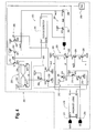
- FIG. 4 One embodiment of an integrated circuit, generally designated 200, is illustrated in Fig. 4.
- this embodiment comprises at least a voltage detect circuit or module, generally designated 202, adapted to detect when a voltage is sufficient to switch the bias conditions without violating the maximum transistor operating conditions for the process; a comparator or comparator circuit or module, generally designated 230, adapted to determine when the PAD voltage is greater than the IO power supply voltage; a switching transistor device or module 262; input circuit or module 264; a tri-state circuit or module 212 adapted to ensure one or more device(s) coupled to at least the PAD will not turn on when the PAD voltage exceeds the IO power supply voltage: an overstress prevention circuit, 203, designed to prevent overstress when the output is disabled and the pad is driven to 5V.
- an overstress prevention circuit 203, designed to prevent overstress when the output is disabled and the pad is driven to 5V.
- an overstress circuit or module prevents overstressing devices 238 and 240 of the circuit 200 when the floating well (alternatively referred to as "fw") is greater than or equal to the higher of the PAD voltage or the highest voltage in the circuit (i.e., VDDO).
- the overstress circuit 203 may prevent such overstress enabling the source of device 236 to rise to VDDO-V t (the threshold of an NMOS device), when node fw > VDDO.
- the overstress circuit 203 comprises at least one, but generally three, transistor devices, such as three NMOS or n-channel transistor devices 236, 238 and 240 for example.
- the voltage detect circuit 202 is adapted to detect when a voltage is sufficient to switch the bias conditions without violating maximum transistor operating conditions for the process.
- the voltage detect circuit comprises a voltage detect device 246 having an input coupled to device 248 and node "inp", an output labeled "out” coupled to node p3h, and PMOS devices 242 and 252, and output labeled "outb” coupled to NMOS device 240 and PMOS device 244.
- the voltage detect device 246 is adapted to determine whether the PAD voltage is high or low (i.e., in one embodiment the input node inp and output node p3h of the detect device 246 are the same logic state and output node p2h is the opposite logic state of output node p3h).
- the integrated circuit 200 also comprises the comparator circuit or module 230 adapted to determine when the PAD voltage is greater than the IO power supply voltage.
- the comparator 230 comprises at least one, but generally two or more devices, such as two PMOS or p-channel transistor devices 232 and 234 for example.
- This embodiment further comprises tri-state circuit or module 212 adapted to guarantee that a device, such as a PMOS or p-channel transistor device 222 for example, will not turn on when the PAD voltage exceeds the IO power supply voltage.
- the tri-state circuit 212 comprises at least one, but generally three, devices, such as a PMOS or p-channel transistor device 214 and two NMOS or n-channel transistor devices 216 and 218.
- One embodiment of the present invention comprises at least one, but generally two or more power supplies. Such power supplies may be externally supplied or generated internally. In the illustrated embodiment, three power supplies are contemplated; the core power supply or VDDC, the intermediate power supply, or VDDP, and the IO power supply or VDDO. VDDP is set to the maximum IO device voltage (i.e., less than VDDO for example). It is contemplated that utilizing 3 power supplies, limits the maximum voltage across any device, maintaining gate oxide reliability and avoiding hot carrier injection (alternatively referred to as "HCI").
- HCI hot carrier injection
- the circuit 200 further comprises a node sw23, coupled to at least one but generally two or more devices, PMOS or p-channel transistor 242 and 244 for example.
- Node sw23 and devices 242 and 244 are adapted to pull the gates of the transistor devices 224 and 250 to VDDO if the PAD voltage is high, and to VDDP if the PAD voltage is low.
- PAD 256 is illustrated coupled to transistor device 250 and to sw23 through circuit 202 and devices 242 and 244.
- the circuit 200 further comprises a pre-driver logic device 210, which is adapted to generate one or more logic states that drive the stacked output devices, 220 and 226.
- the pre-driver logic device 210 is coupled to nodes 253 (alternatively referred to as "data") and node 254 (alternatively referred to as “oe” or “output enable”), and the gates of the stacked output devices, 220 and 226.
- nodes data and oe are coupled from the core circuitry (not shown).
- the output device circuit or module 260 comprise at least one, but generally two or more transistor devices, for example two PMOS transistor devices 220 and 222, and two NMOS devices 224 and 226, where devices 222 and 224 are coupled to the PAD 256.
- Node oe 254 drives the gate of transistor device 218 turning device 218 on. Turning device 218 on pulls the node pt to VDDC. When node pt reaches VDDC, PAD 256 may switch between VSSC and VDDO without causing overstress on transistor device 222.
- transistor device 242 When node p3h reaches VDDC, transistor device 242 is turned on and node sw23 is pulled to VDDP. When node sw23 reaches VDDP, the gate of transistor devices 250 and 224 are driven to VDDP, lowering the voltage across transistor devices 250 and 224 when the PAD Voltage is driven to VSSC. In one embodiment of the present invention, transistor device 252 decouples the PAD 256 (and the PAD voltage) from the gate of transistor device 232 when the PAD voltage is less than VDDO+Vt. This prevents overstress on transistor device 232 when the PAD voltage is driven to VSSC.
- Transistor devices 238 and 236 are added to pull the gate of transistor device 232 to VDDC when node oe is enabled, preventing overstress on device 232.
- transistor device 224 is on and 226 is off and transistor devices 220 and 222 are turned on.
- Turning on devices 220 and 222 drives the PAD voltage to VDDO.
- the PAD voltage is communicated or fed back through the voltage detector 246, resulting in node p3h being driven to VDDO and node p2h being driven to VDDC.
- transistor device 244 is turned on and node sw23 is driven to VDDO.
- node sw23 reaches VDDO, the gates of devices 250 and 224 are driven to VDDO, lowering the voltage across transistor devices 250 and 224 when PAD is driven to VDDO.
- node oe 254 drives the gate of transistor devices 238, turning device 238 on or off.
- transistor devices 218 and 238 are off.
- Transistor devices 224, 226, 220, 222 and hence the PAD node are driven to a high impedance state.
- the PAD node may, in this embodiment, be driven by an external bus.
- the bus drives PAD 256 to VSSC.
- the PAD voltage is communicated or fed back through the voltage detector 246 resulting in node p3h being driven to VDDC and node p2h being driven to VDDO.
- transistor device 242 is turned on and node sw23 is driven to VDDP.
- Node sw23 drives the gates of devices 250 and 224 to VDDP, lowering the voltage across devices 250 and 224 when the PAD Voltage is driven to VSSC.
- node p2h When node p2h is driven to VDDO, it turns on the device 240 pulling the gate of transistor device 232 low. Pulling the gate of device 232 low turns it on, pulling node fw to VDDO.
- PAD 256 is coupled to transistor device 252.
- Device 252 turns on when PAD Voltage is at >VDDO + Vt and the gate of device 252 is at VDDO, which pulls the gate of transistor device 232 to the PAD voltage, turning off device 232, turning on device 234 and pulling node fw to PAD.
- transistor device 214 turns on, pulling node pt to the fw node or the PAD voltage. This prevents voltage stress on device 222 and keeps node PAD in high impendance state.
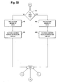
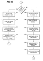
- Figs. 5A, 5B, 5C, 6A, 6B, 6C and 6D illustrate methods of operating a core circuit of an integrated circuit at a lower voltage than the coupled IO circuitry using a voltage tolerant circuit in accordance with the present invention.
- the method comprises using a voltage tolerant circuit (a 5V tolerant circuit for example) to prevent overstress on at least one device of a circuit when the floating well or fw equal to the higher of the PAD voltage or the highest voltage in the circuit (VDDO for example).
- a voltage tolerant circuit a 5V tolerant circuit for example
- the voltage tolerant circuit operates in one or more possible operating conditions.
- Figs. 5A, 5B and 5C illustrate a high level flow chart depicting a method of operating a core circuit of an integrated circuit at a lower voltage than the coupled IO circuitry using a voltage tolerant circuit (a 5V tolerant circuit for example) in accordance with the present invention, generally designated 400.
- the PAD voltage is driven to VDDO as illustrated by block 426.
- the gates of devices 250 and 224 are driven to VDDO, lowering the voltage across transistor devices 250 and 224 as illustrated by block 428.
- the bus drives the PAD voltage to > VDDO + Vt as illustrated by block 450.
- the gates of transistor devices 250 and 224 are driven to VDDO, lowering the voltage across devices 250 and 224 as illustrated by block 452.
- Node fw is pulled to the PAD voltage as illustrated by block 456.
- transistor device 214 turns on, pulling node pt to the voltage of node fw or the PAD Voltage as illustrated by block 458.
- Device 216 prevents voltage stress on device 218 and overstress is prevented on device 222 as illustrated by blocks 459 and 460.
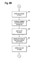
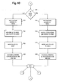
- Figs. 6A, 6B, 6C and 6D illustrate a flow chart depicting one method of operating a core circuit of an integrated circuit at a lower voltage than the coupled IO circuitry using a voltage tolerant circuit (a 5V tolerant circuit for example) in accordance with the present invention, generally designated 500.
- method 500 comprises determining if node oe is enabled as illustrated by diamond 510. If node oe is enabled, the gate of device 232 is pulled to VDDC as illustrated by block 509 and voltage stress is prevented on device 232 as illustrated by block 511. Node fw is pulled to VDDO as illustrated by block 512.
- node 254 drives the gate of transistor device 238, turning device 238 on, which pulls down the gate of transistor device 232, turning device 232 on and pulling node fw equal to VDDO as illustrated by block 512.
- VDDO is the highest voltage seen by the circuit.
- Node pt is pulled to VDDC as illustrated by block 514.
- node oe drives the gate of transistor device 218 turning device 218 on which pulls the node pt to VDDC.
- the PAD voltage may switch between VSSC and VDDO without causing overstress on transistor device 222 as illustrated by blocks 516 and 518.
- the PAD voltage is communicated or fed back through the voltage detector 246, resulting in nodes p3h being pulled to VDDC and p2h being pulled to VDDO as illustrated by block 524.
- transistor device 242 is turned on and node sw23 is pulled to VDDP as illustrated by block 526.
- node sw23 reaches VDDP the gate of transistor devices 250 and 224 are driven to VDDP, lowering the voltage across transistor devices 250 and 224 as illustrated by block 528.
- transistor device 252 decouples the PAD Voltage from the gate of transistor device 232 when the PAD voltage is less than VDDO+Vt.
- transistor device 226 is off and transistor devices 220 and 222 are turned on, which drives the PAD voltage to VDDO as illustrated by block 534.
- the PAD voltage is communicated or fed back through the voltage detector 246, resulting in node p3h being driven to VDDO and node p2h being driven to VDDC as illustrated by block 536.
- Node sw23 is pulled to VDDO as illustrated by block 538.
- transistor device 244 when node p2h reaches VDDC, transistor device 244 is turned on and node sw23 is driven to VDDO as illustrated by block 538. When node sw23 reaches VDDO, the gates of devices 250 and 224 are driven to VDDO, lowering the voltage across transistor devices 250 and 224 as illustrated by block 540.
- the PAD Voltage is driven to VSSO by the bus as illustrated by block 550.
- Node sw23 is driven to VDDP as illustrated by block 552.
- the PAD voltage is communicated or fed back through the voltage detector 246 resulting in node p3h being driven to VDDC and node p2h being driven to VDDO.
- transistor device 242 is turned on and node sw23 is driven to VDDP.
- Node sw23 drives the gates of devices 250 and 224 to VDDP, lowering the voltage across devices 250 and 224 as illustrated by block 554. Further, when node p2h is driven to VDDO, it turns on the device 240 pulling the gate of transistor device 232 low. Pulling the gate of device 232 low turns it on, pulling node fw to VDDO as illustrated in blocks 580, 581 and 582.
- Method 500 further comprises determining if node oe is not enabled and the PAD Voltage ⁇ VDDO + Vt as illustrated by diamond 556.
- Block 557 illustrates that, when node oe is not enabled, the bus drives the PAD Voltage to ⁇ VDDO + Vt.
- the PAD voltage is communicated or fed back through the voltage detector 246, resulting in node p3h being driven to VDDO and node p2h being driven to VDDC.
- transistor device 244 is turned on and sw23 is driven to VDDO as illustrated by block 558.
- Node sw23 drives the gates of transistor devices 250 and 224 to VDDO, lowering the voltage across devices 250 and 224 as illustrated by block 560.
- node fw floats between VDDO ⁇ Vt due to transistor device 232 and the drain to bulk diode, fw, of device 222 as illustrated by block 562.
- method 500 comprises determining if node oe is not enabled and the PAD Voltage > VDDO + Vt as illustrated by diamond 556.
- the bus drives the PAD voltage to > VDDO + Vt as illustrated by block 566.
- the PAD voltage is communicated or fed back through the voltage detector 246, such that node p3h is driven to VDDO and node p2h is driven to VDDC.
- transistor device 244 is turned on and node sw23 is driven to VDDO as illustrated by block 568.
- Node sw23 drives the gates of transistor devices 250 and 224 to VDDO, lowering the voltage across devices 250 and 224 as illustrated by block 570.
- Transistor device 252 turns on as the PAD Voltage is at > VDDO + Vt and the gate of device 252 is at VDDO, which pulls the gate of transistor device 232 to the PAD voltage, turning it off and device 234 on, pulling node fw to the PAD voltage as illustrated by block 572.
- transistor device 214 turns on, pulling node pt to the voltage of node fw or the PAD Voltage as illustrated by block 574. This prevents voltage stress on device 222 as illustrated by block 576.
- HCI may be significantly reduced when the output transitions from dissabled to enabled with the pad at 5.5V and the data is low. For example, if the pad is at 5.5V and the enable goes from low to high, with the data low, there will be a very large Vds on devices 224 and 226 resulting in possible HCI stress since 224 and 226 are on.
- the tolerant circuit the integrated circuit including at least a tolerant circuit and a method of operating a core circuit of an integrated circuit at a lower voltage than the coupled IO circuitry using a tolerant circuit in accordance with the present invention provides/includes one or more of the following advantages and features: (1) enables lower power higher speed and more efficient design of core/analog while still utilizing 5V tolerant IOs; (2) simplifies fabrication process and cost as three gate oxides may no longer be needed for optimum performance and 5V tolerance; and (3) reduces HCI stress on the NMOS output driver; and (4) Allows the use of the more efficient 2.5V device, while still enabling the output pad to be driven by a 5V bus
- One embodiment eliminates the tri-state circuit 212 and ties node pt to the gate of device 232.
Landscapes
- Physics & Mathematics (AREA)
- Engineering & Computer Science (AREA)
- Computer Hardware Design (AREA)
- Computing Systems (AREA)
- General Engineering & Computer Science (AREA)
- Mathematical Physics (AREA)
- Semiconductor Integrated Circuits (AREA)
- Logic Circuits (AREA)
Abstract
Description
| Output | DATA | PAD | |
| 1 | 0 | 0 | |
| 1 | 1 | 1 | |
| 0 | 0 | | |
| 0 | 1 | Z |
Claims (20)
- A voltage tolerant circuit comprising:a voltage detect module adapted to detect when a voltage is sufficient to switch bias conditions without violating maximum transistor operating conditions; anda comparator adapted to detect when a PAD voltage is greater than an 10 power supply voltage.
- The voltage tolerant circuit of Claim 1, wherein said voltage detect module comprises a voltage detect device adapted to determine whether said PAD voltage is high or low.
- The voltage tolerant circuit of Claim 1, wherein said comparator comprises at least one device.
- The voltage tolerant circuit of Claim 1, wherein said comparator comprises two PMOS transistor devices.
- The voltage tolerant circuit of Claim 1, further comprising a tri-state module adapted to ensure that a PMOS transistor device will not turn on when said pad voltage exceeds said IO power supply voltage.
- The voltage tolerant circuit of Claim 5, wherein said tri-state module comprises at least one device.
- The voltage tolerant circuit of Claim 5, wherein said tri-state module comprises at least one PMOS transistor device.
- The voltage tolerant circuit of Claim 5, wherein said tri-state module comprises at least one NMOS transistor device.
- The voltage tolerant circuit of Claim 1, further comprising an overstress module.
- The voltage tolerant circuit of Claim 9, wherein said overstress module comprises at least one device.
- The voltage tolerant circuit of Claim 9, wherein said overstress module comprises three NMOS transistor devices.
- The voltage tolerant circuit of Claim 9, wherein said overstress module is further adapted to prevent at least one transistor device from being overstressed.
- The voltage tolerant circuit of Claim 12, wherein said overstress module prevents said overstress when a voltage of a floating well is greater than said PAD Voltage.
- The voltage tolerant circuit of Claim 12, wherein said overstress module prevents said overstress when a voltage of a floating well is greater than said IO Power Supply Voltage.
- The voltage tolerant circuit of Claim 1, further comprising a switching transistor device adapted to switch between an intermediate power voltage and an IO power voltage.
- The voltage tolerant circuit of Claim 1, further comprising a transistor device adapted to decouple said PAD Voltage from at least one device in said comparator when said PAD voltage is less than a predetermined voltage.
- The voltage tolerant circuit of Claim 1, wherein said predetermined voltage comprises a voltage of a core power supply plus a threshold voltage of said voltage detect circuit.
- A voltage tolerant circuit comprising:a voltage detect module adapted to detect when a voltage is sufficient to switch bias conditions without violating maximum transistor operating conditions;a comparator adapted to detect when a PAD voltage is greater than an IO power supply voltage;a tri-state module adapted to ensure that a PMOS transistor device will not turn on when said pad voltage exceeds said IO power supply voltage; andan overstress module adapted to prevent overstress of at least one device in a comparator module.
- An integrated circuit comprising:core circuitry;a PAD device; anda voltage tolerant circuit coupled to said core circuitry and said PAD device, said voltage tolerant circuit comprising:a voltage detect module adapted to detect when a voltage is sufficient to switch bias conditions without violating maximum transistor operating conditions; anda comparator adapted to detect when a PAD voltage is greater than an IO power supply voltage.
- A method of operating an integrated circuit using a voltage tolerant circuit comprising:a step of detecting when a voltage is sufficient to switch bias conditions without violating maximum transistor operating conditions using a voltage detect module of the voltage tolerant circuit; anda step of detecting when a PAD voltage is greater than an IO power supply voltage using a comparator of the voltage detect circuit.
Applications Claiming Priority (4)
| Application Number | Priority Date | Filing Date | Title |
|---|---|---|---|
| US40277102P | 2002-08-12 | 2002-08-12 | |
| US10/370,392 US6856168B2 (en) | 2002-08-12 | 2003-02-19 | 5 Volt tolerant IO scheme using low-voltage devices |
| US370392 | 2003-02-19 | ||
| US402771P | 2010-09-03 |
Publications (2)
| Publication Number | Publication Date |
|---|---|
| EP1389832A1 true EP1389832A1 (en) | 2004-02-18 |
| EP1389832B1 EP1389832B1 (en) | 2009-07-29 |
Family
ID=30772803
Family Applications (1)
| Application Number | Title | Priority Date | Filing Date |
|---|---|---|---|
| EP03018263A Expired - Lifetime EP1389832B1 (en) | 2002-08-12 | 2003-08-11 | 5 volt tolerant IO scheme using low-voltage devices |
Country Status (3)
| Country | Link |
|---|---|
| US (2) | US6856168B2 (en) |
| EP (1) | EP1389832B1 (en) |
| DE (1) | DE60328568D1 (en) |
Cited By (1)
| Publication number | Priority date | Publication date | Assignee | Title |
|---|---|---|---|---|
| EP3053271B1 (en) * | 2013-10-01 | 2025-06-25 | Texas Instruments Incorporated | Controlling current during power-up and power -down sequences |
Families Citing this family (13)
| Publication number | Priority date | Publication date | Assignee | Title |
|---|---|---|---|---|
| US7236002B2 (en) * | 2005-09-15 | 2007-06-26 | Dialog Semiconductor Gmbh | Digital CMOS-input with N-channel extended drain transistor for high-voltage protection |
| US8238068B2 (en) * | 2009-04-24 | 2012-08-07 | Silicon Laboratories Inc. | Electrical over-stress detection circuit |
| US9166591B1 (en) | 2012-02-03 | 2015-10-20 | Altera Corporation | High speed IO buffer |
| KR101993192B1 (en) | 2012-10-04 | 2019-06-27 | 삼성전자주식회사 | Multi-voltage supplied input buffer |
| US9391618B2 (en) * | 2014-08-06 | 2016-07-12 | Broadcom Corporation | High voltage fail-safe IO design using thin oxide devices |
| US9871373B2 (en) | 2015-03-27 | 2018-01-16 | Analog Devices Global | Electrical overstress recording and/or harvesting |
| US10557881B2 (en) | 2015-03-27 | 2020-02-11 | Analog Devices Global | Electrical overstress reporting |
| US10090838B2 (en) * | 2015-09-30 | 2018-10-02 | Silicon Laboratories Inc. | Over voltage tolerant circuit |
| US10365322B2 (en) | 2016-04-19 | 2019-07-30 | Analog Devices Global | Wear-out monitor device |
| US10338132B2 (en) | 2016-04-19 | 2019-07-02 | Analog Devices Global | Wear-out monitor device |
| US11024525B2 (en) | 2017-06-12 | 2021-06-01 | Analog Devices International Unlimited Company | Diffusion temperature shock monitor |
| TWI847475B (en) * | 2023-01-05 | 2024-07-01 | 瑞昱半導體股份有限公司 | Input circuit having adaptive voltage-receiving mechanism |
| TW202437699A (en) | 2023-03-01 | 2024-09-16 | 聯華電子股份有限公司 | Input/output circuit |
Citations (3)
| Publication number | Priority date | Publication date | Assignee | Title |
|---|---|---|---|---|
| EP0862267A2 (en) * | 1997-02-07 | 1998-09-02 | Silicon Systems Research Ltd. | 5V tolerant I/O circuit |
| US6081412A (en) * | 1998-07-20 | 2000-06-27 | National Semiconductor Corporation | Gate oxide breakdown protection circuit for deep submicron processes |
| US6130556A (en) * | 1998-06-16 | 2000-10-10 | Lsi Logic Corporation | Integrated circuit I/O buffer with 5V well and passive gate voltage |
Family Cites Families (13)
| Publication number | Priority date | Publication date | Assignee | Title |
|---|---|---|---|---|
| US5406140A (en) * | 1993-06-07 | 1995-04-11 | National Semiconductor Corporation | Voltage translation and overvoltage protection |
| US5543733A (en) * | 1995-06-26 | 1996-08-06 | Vlsi Technology, Inc. | High voltage tolerant CMOS input/output circuit |
| US5721508A (en) | 1996-01-24 | 1998-02-24 | Cypress Semiconductor Corporation | 5 Volt tolerant 3.3 volt output buffer |
| US5825206A (en) * | 1996-08-14 | 1998-10-20 | Intel Corporation | Five volt safe output buffer circuit that controls the substrate and gates of the pull-up devices |
| US6028450A (en) * | 1998-03-17 | 2000-02-22 | Xilinx, Inc. | Programmable input/output circuit with pull-up bias control |
| US6018257A (en) | 1998-03-23 | 2000-01-25 | Lsi Logic Corporation | Output drive circuit tolerant of higher voltage signals |
| US6118301A (en) * | 1998-05-26 | 2000-09-12 | Analog Devices, Inc. | High voltage tolerant and compliant driver circuit |
| US6265926B1 (en) * | 1998-05-27 | 2001-07-24 | Altera Corporation | Programmable PCI overvoltage input clamp |
| US6388469B1 (en) * | 1999-08-13 | 2002-05-14 | Cypress Semiconductor Corp. | Multiple power supply output driver |
| US6414515B1 (en) * | 1999-12-20 | 2002-07-02 | Texas Instruments Incorporated | Failsafe interface circuit with extended drain devices |
| US6388470B1 (en) * | 2000-03-30 | 2002-05-14 | Philips Electronics North American Corporation | High voltage CMOS signal driver with minimum power dissipation |
| WO2002056473A2 (en) * | 2001-01-09 | 2002-07-18 | Broadcom Corp | Sub-micron high input voltage tolerant input output (i/o) circuit |
| US6803789B1 (en) * | 2002-10-04 | 2004-10-12 | Semiconductor Manufacturing International Corporation | High voltage tolerant output buffer |
-
2003
- 2003-02-19 US US10/370,392 patent/US6856168B2/en not_active Expired - Lifetime
- 2003-08-11 EP EP03018263A patent/EP1389832B1/en not_active Expired - Lifetime
- 2003-08-11 DE DE60328568T patent/DE60328568D1/en not_active Expired - Lifetime
-
2005
- 2005-02-04 US US11/051,146 patent/US7521965B2/en not_active Expired - Fee Related
Patent Citations (3)
| Publication number | Priority date | Publication date | Assignee | Title |
|---|---|---|---|---|
| EP0862267A2 (en) * | 1997-02-07 | 1998-09-02 | Silicon Systems Research Ltd. | 5V tolerant I/O circuit |
| US6130556A (en) * | 1998-06-16 | 2000-10-10 | Lsi Logic Corporation | Integrated circuit I/O buffer with 5V well and passive gate voltage |
| US6081412A (en) * | 1998-07-20 | 2000-06-27 | National Semiconductor Corporation | Gate oxide breakdown protection circuit for deep submicron processes |
Cited By (1)
| Publication number | Priority date | Publication date | Assignee | Title |
|---|---|---|---|---|
| EP3053271B1 (en) * | 2013-10-01 | 2025-06-25 | Texas Instruments Incorporated | Controlling current during power-up and power -down sequences |
Also Published As
| Publication number | Publication date |
|---|---|
| EP1389832B1 (en) | 2009-07-29 |
| US20040027159A1 (en) | 2004-02-12 |
| DE60328568D1 (en) | 2009-09-10 |
| US6856168B2 (en) | 2005-02-15 |
| US7521965B2 (en) | 2009-04-21 |
| US20050127953A1 (en) | 2005-06-16 |
Similar Documents
| Publication | Publication Date | Title |
|---|---|---|
| US6040708A (en) | Output buffer having quasi-failsafe operation | |
| EP0663727B1 (en) | Output buffer circuit, input buffer circuit and bi-directional buffer circuit for plural voltage systems | |
| EP1356590B1 (en) | Sub-micron high input voltage tolerant input output (i/o) circuit | |
| US6856168B2 (en) | 5 Volt tolerant IO scheme using low-voltage devices | |
| US6353333B1 (en) | Simplified 5V tolerance circuit for 3.3V I/O design | |
| US20040105201A1 (en) | Scheme for eliminating the channel unexpected turn-on during ESD zapping | |
| JPH08237102A (en) | I / O buffer circuit device | |
| US5914844A (en) | Overvoltage-tolerant input-output buffers having a switch configured to isolate a pull up transistor from a voltage supply | |
| US7978001B2 (en) | Microprocessor with selective substrate biasing for clock-gated functional blocks | |
| US6580291B1 (en) | High voltage output buffer using low voltage transistors | |
| US6265931B1 (en) | Voltage reference source for an overvoltage-tolerant bus interface | |
| US20080106836A1 (en) | Io clamping circuit method utilizing output driver transistors | |
| EP0874462B1 (en) | Pull-up circuit and semiconductor device using the same | |
| US6222387B1 (en) | Overvoltage tolerant integrated circuit input/output interface | |
| US7199612B2 (en) | Method and circuit for reducing HCI stress | |
| US5903180A (en) | Voltage tolerant bus hold latch | |
| US7920019B2 (en) | Microprocessor with substrate bias clamps | |
| JP3940743B2 (en) | Semiconductor integrated circuit device and level conversion circuit | |
| EP0735686B1 (en) | Three-state CMOS output buffer circuit | |
| EP1389833B1 (en) | Method and circuit for reducing hot-carrier injection stress | |
| JP4473293B2 (en) | Semiconductor device input / output circuit | |
| JP4034178B2 (en) | Output buffer circuit | |
| JP3801519B2 (en) | Output buffer circuit | |
| US10541684B2 (en) | Input/output circuit | |
| JP3983704B2 (en) | Output buffer circuit |
Legal Events
| Date | Code | Title | Description |
|---|---|---|---|
| PUAI | Public reference made under article 153(3) epc to a published international application that has entered the european phase |
Free format text: ORIGINAL CODE: 0009012 |
|
| AK | Designated contracting states |
Kind code of ref document: A1 Designated state(s): AT BE BG CH CY CZ DE DK EE ES FI FR GB GR HU IE IT LI LU MC NL PT RO SE SI SK TR |
|
| AX | Request for extension of the european patent |
Extension state: AL LT LV MK |
|
| 17P | Request for examination filed |
Effective date: 20040818 |
|
| AKX | Designation fees paid |
Designated state(s): DE FR GB |
|
| RAP1 | Party data changed (applicant data changed or rights of an application transferred) |
Owner name: BROADCOM CORPORATION |
|
| 17Q | First examination report despatched |
Effective date: 20070913 |
|
| GRAP | Despatch of communication of intention to grant a patent |
Free format text: ORIGINAL CODE: EPIDOSNIGR1 |
|
| GRAS | Grant fee paid |
Free format text: ORIGINAL CODE: EPIDOSNIGR3 |
|
| GRAA | (expected) grant |
Free format text: ORIGINAL CODE: 0009210 |
|
| AK | Designated contracting states |
Kind code of ref document: B1 Designated state(s): DE FR GB |
|
| REG | Reference to a national code |
Ref country code: GB Ref legal event code: FG4D |
|
| REF | Corresponds to: |
Ref document number: 60328568 Country of ref document: DE Date of ref document: 20090910 Kind code of ref document: P |
|
| PLBE | No opposition filed within time limit |
Free format text: ORIGINAL CODE: 0009261 |
|
| STAA | Information on the status of an ep patent application or granted ep patent |
Free format text: STATUS: NO OPPOSITION FILED WITHIN TIME LIMIT |
|
| 26N | No opposition filed |
Effective date: 20100503 |
|
| REG | Reference to a national code |
Ref country code: FR Ref legal event code: ST Effective date: 20110502 |
|
| PG25 | Lapsed in a contracting state [announced via postgrant information from national office to epo] |
Ref country code: FR Free format text: LAPSE BECAUSE OF NON-PAYMENT OF DUE FEES Effective date: 20090929 |
|
| PGFP | Annual fee paid to national office [announced via postgrant information from national office to epo] |
Ref country code: GB Payment date: 20160830 Year of fee payment: 14 |
|
| REG | Reference to a national code |
Ref country code: DE Ref legal event code: R082 Ref document number: 60328568 Country of ref document: DE Representative=s name: BOSCH JEHLE PATENTANWALTSGESELLSCHAFT MBH, DE Ref country code: DE Ref legal event code: R081 Ref document number: 60328568 Country of ref document: DE Owner name: AVAGO TECHNOLOGIES INTERNATIONAL SALES PTE. LT, SG Free format text: FORMER OWNER: BROADCOM CORP., IRVINE, CALIF., US Ref country code: DE Ref legal event code: R081 Ref document number: 60328568 Country of ref document: DE Owner name: AVAGO TECHNOLOGIES GENERAL IP (SINGAPORE) PTE., SG Free format text: FORMER OWNER: BROADCOM CORP., IRVINE, CALIF., US |
|
| REG | Reference to a national code |
Ref country code: GB Ref legal event code: 732E Free format text: REGISTERED BETWEEN 20171005 AND 20171011 |
|
| GBPC | Gb: european patent ceased through non-payment of renewal fee |
Effective date: 20170811 |
|
| PG25 | Lapsed in a contracting state [announced via postgrant information from national office to epo] |
Ref country code: GB Free format text: LAPSE BECAUSE OF NON-PAYMENT OF DUE FEES Effective date: 20170811 |
|
| REG | Reference to a national code |
Ref country code: DE Ref legal event code: R082 Ref document number: 60328568 Country of ref document: DE Representative=s name: BOSCH JEHLE PATENTANWALTSGESELLSCHAFT MBH, DE Ref country code: DE Ref legal event code: R081 Ref document number: 60328568 Country of ref document: DE Owner name: AVAGO TECHNOLOGIES INTERNATIONAL SALES PTE. LT, SG Free format text: FORMER OWNER: AVAGO TECHNOLOGIES GENERAL IP (SINGAPORE) PTE. LTD., SINGAPORE, SG |
|
| PGFP | Annual fee paid to national office [announced via postgrant information from national office to epo] |
Ref country code: DE Payment date: 20200831 Year of fee payment: 18 |
|
| REG | Reference to a national code |
Ref country code: DE Ref legal event code: R119 Ref document number: 60328568 Country of ref document: DE |
|
| PG25 | Lapsed in a contracting state [announced via postgrant information from national office to epo] |
Ref country code: DE Free format text: LAPSE BECAUSE OF NON-PAYMENT OF DUE FEES Effective date: 20220301 |