EP1389805A1 - Multi-slit actuator, ink jet head, and method of manufacturing multi-slit actuator - Google Patents
Multi-slit actuator, ink jet head, and method of manufacturing multi-slit actuator Download PDFInfo
- Publication number
- EP1389805A1 EP1389805A1 EP02714486A EP02714486A EP1389805A1 EP 1389805 A1 EP1389805 A1 EP 1389805A1 EP 02714486 A EP02714486 A EP 02714486A EP 02714486 A EP02714486 A EP 02714486A EP 1389805 A1 EP1389805 A1 EP 1389805A1
- Authority
- EP
- European Patent Office
- Prior art keywords
- piezoelectric material
- slit
- material green
- comb teeth
- multislit
- Prior art date
- Legal status (The legal status is an assumption and is not a legal conclusion. Google has not performed a legal analysis and makes no representation as to the accuracy of the status listed.)
- Granted
Links
Images




Classifications
-
- B—PERFORMING OPERATIONS; TRANSPORTING
- B41—PRINTING; LINING MACHINES; TYPEWRITERS; STAMPS
- B41J—TYPEWRITERS; SELECTIVE PRINTING MECHANISMS, i.e. MECHANISMS PRINTING OTHERWISE THAN FROM A FORME; CORRECTION OF TYPOGRAPHICAL ERRORS
- B41J2/00—Typewriters or selective printing mechanisms characterised by the printing or marking process for which they are designed
- B41J2/005—Typewriters or selective printing mechanisms characterised by the printing or marking process for which they are designed characterised by bringing liquid or particles selectively into contact with a printing material
- B41J2/01—Ink jet
- B41J2/135—Nozzles
- B41J2/16—Production of nozzles
- B41J2/1607—Production of print heads with piezoelectric elements
- B41J2/1609—Production of print heads with piezoelectric elements of finger type, chamber walls consisting integrally of piezoelectric material
-
- B—PERFORMING OPERATIONS; TRANSPORTING
- B41—PRINTING; LINING MACHINES; TYPEWRITERS; STAMPS
- B41J—TYPEWRITERS; SELECTIVE PRINTING MECHANISMS, i.e. MECHANISMS PRINTING OTHERWISE THAN FROM A FORME; CORRECTION OF TYPOGRAPHICAL ERRORS
- B41J2/00—Typewriters or selective printing mechanisms characterised by the printing or marking process for which they are designed
- B41J2/005—Typewriters or selective printing mechanisms characterised by the printing or marking process for which they are designed characterised by bringing liquid or particles selectively into contact with a printing material
- B41J2/01—Ink jet
- B41J2/135—Nozzles
- B41J2/16—Production of nozzles
- B41J2/1621—Manufacturing processes
- B41J2/1632—Manufacturing processes machining
-
- H—ELECTRICITY
- H10—SEMICONDUCTOR DEVICES; ELECTRIC SOLID-STATE DEVICES NOT OTHERWISE PROVIDED FOR
- H10N—ELECTRIC SOLID-STATE DEVICES NOT OTHERWISE PROVIDED FOR
- H10N30/00—Piezoelectric or electrostrictive devices
- H10N30/01—Manufacture or treatment
- H10N30/08—Shaping or machining of piezoelectric or electrostrictive bodies
- H10N30/085—Shaping or machining of piezoelectric or electrostrictive bodies by machining
- H10N30/089—Shaping or machining of piezoelectric or electrostrictive bodies by machining by punching
-
- H—ELECTRICITY
- H10—SEMICONDUCTOR DEVICES; ELECTRIC SOLID-STATE DEVICES NOT OTHERWISE PROVIDED FOR
- H10N—ELECTRIC SOLID-STATE DEVICES NOT OTHERWISE PROVIDED FOR
- H10N39/00—Integrated devices, or assemblies of multiple devices, comprising at least one piezoelectric, electrostrictive or magnetostrictive element covered by groups H10N30/00 – H10N35/00
-
- H—ELECTRICITY
- H02—GENERATION; CONVERSION OR DISTRIBUTION OF ELECTRIC POWER
- H02N—ELECTRIC MACHINES NOT OTHERWISE PROVIDED FOR
- H02N2/00—Electric machines in general using piezoelectric effect, electrostriction or magnetostriction
- H02N2/02—Electric machines in general using piezoelectric effect, electrostriction or magnetostriction producing linear motion, e.g. actuators; Linear positioners ; Linear motors
- H02N2/021—Electric machines in general using piezoelectric effect, electrostriction or magnetostriction producing linear motion, e.g. actuators; Linear positioners ; Linear motors using intermittent driving, e.g. step motors, piezoleg motors
Definitions
- the present invention relates to amultislit type actuator formed by aligning and allocating a plurality of actuators made of a piezoelectric material in comb teeth shape. Particularly, it relates to a method for manufacturing a multislit type actuator allowing mass production with no need of cleaning to drying process and in which slits having a width of 50 ⁇ m or less or having an aspect ratio of 10 or more can be formed, and a multislit type actuator hardly generating the destruction of crystal grains in the wall surfaces of the slits formed by the manufacturing method, and an inkjet head.
- a shear mode piezoelectric actuator for use in an inkjet head.
- This has the structure as shown in Fig. 11 in which a plurality of wall parts 22 made of a piezoelectric material formed of comb teeth shape on a substrate 21, rectangular ink chambers 23 adjacently formed between the wall parts, and the wall parts 22 deformed to vary the volume of the ink chambers for discharge operation.
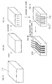
- Such the actuator is formed by the steps shown in Fig. 7.
- a piezoelectric material 17 is prepared in Fig. 7A, and is fired in Fig. 7B.
- the piezoelectric material are polarized in Fig. 7C.
- fine slits are formed by a dicing saw and the like to form driving portions 18 in comb teeth shape and a plurality of slits 19 for storing ink is formed and arranged in Fig. 7D.
- electrodes 20 are formed on the wall surfaces inside the slits in Fig. 7E.
- the ink chambers are closed with a cover plate 24 made of a glass plate and the like, and the opening parts at the tip ends are closed with a nozzle plate 25 formed with nozzles 26.
- the corner parts tend to be chipped because a hard plate made of piezoelectric material is machined, having the following problems.
- limitation is imposed on the slits being the ink chamber by a dicer blade used for machining, not allowing a width of about 70 ⁇ m or less.
- a limit value is self-determined to a depth of the slits because the wall thickness also requires the strength against the dicer blade cutting, and it is difficult to form at an aspect ratio of 10 or more. On this account, it is impossible to obtain a comb-tooth type actuator of high density, or of high strength and high power output.
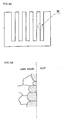
- Fig. 8 is an explanatory drawing illustrating this.
- Fig. 8A is an end view illustrating seen from Q shown in Fig. 7, and
- Fig. 8B is an enlarged sectional view of N part.
- a part thereof is chipped by cutting with the dicing saw to generate transgranular fracture, causing deterioration in the property.
- micro-cracks are occurred between the crystal grains or inside the grains by cutting, sometimes causing deterioration in the property.
- a manuf acturing method shown in Fig. 9 as a me thod without using a dicer blade.
- This is a manufacturing method that a predetermined number of piezoelectric material green sheets 1 is separately punched in comb teeth in Fig. 9A, a jig is used to align and laminate them on a substrate 4 and they are heated and compressed in Fig. 9B. Then they are fired and integrated in a unitary body in Fig. 9C, polarized in Fig. 9D, and then electrodes 6 and the like are formed in Fig. 9E.
- a method for aligning the green sheets includes the following steps. First, holes for positioning are formed in each of the green sheets 1. Then a jigwithpins for positioning is prepared, and it penetrates the pins through the holes in the green sheets 1 for lamination. In this method, however, a clearance between the hole and the pin is required to be at least 10 ⁇ m. Further, due to the softness of the green sheet 1, an alignment deviation of nearly 20 ⁇ m is inevitably generated between the piezoelectric layers when 10 layers or more are laminated.
- the present invention has been made based on the experimental results. There is provided a multislit type actuator hardly generating the destruction of crystal grains in the wall surfaces of the slits and an inkjet head. Moreover, there is provided a method for manufacturing a multislit type actuator allowing mass production with no need of cleaning to drying process in which slits other than a linear form and slits having a width of 50 ⁇ m or less or having an aspect ratio of 10 or more can be formed.
- a multislit type actuator is characterized by having a plurality of piezoelectric actuators aligned and allocated in comb teeth formed on a substrate, wherein a condition of crystal grains in side surfaces of the piezoelectric actuators forming wall surfaces of a slit between the comb teeth is that the crystal grains under transgranular fracture are 1% or less.
- a surface roughness Rt of the wall surfaces of the slit is 10 ⁇ m or less and an amount of convexo-concave in the wall surfaces of the slit is 10 ⁇ m or less.
- a slit width between the comb teeth may be not a simple linear groove but varied from a back to a tip end of the comb teeth. Consequently, when the slits are used as the ink path of the inkjet head, it is possible to obtain comb teeth shape suitable for fluid, which reduces the piezoelectric deforming stress of the tip end parts of the comb teeth. As a result, a long lifetime can be obtained without interposing another component.
- the slit width between each of the comb teeth is not the same and has at least two kinds of width, and minimum slit width is less than 70 ⁇ m. Consequently, the optimum slit width can be formed in accordance with the purpose, and the actuator having the optimum characteristics can be provided.
- One of the inkjet heads according to the invention there is an inkjet head driven by a shear mode characterized in that a top surface of the actuator opposite to the substrate of the multislit type actuator with the above configuration is closed by a closing plate, and the slit is formed as an ink chamber to allow ink to be discharged in a tip direction of the comb teeth.
- Another inkjet head there is an inkjet head driven by a shear mode characterized in that side surfaces of two multislit type actuators with the above mentioned configuration, are joined so as to align with comb tooth parts each other, and slit parts formed in a chamber shape as ink chambers to allow ink to be discharged in a tip direction of the comb teeth.
- the ink path can be formed in a shape suitable for fluid, and long lifetime can be obtained.
- a method for manufacturing a multislit type actuator according to the invention is a method for manufacturing a multislit type actuator in which a plurality of actuators, each comprising a piezoelectric material, are aligned and allocated on a substrate in the shape of comb teeth, characterized by including, a first process in which a plurality of piezoelectric material green sheets are prepared, and slit apertures are formed on a first piezoelectric material green sheet among the above plural piezoelectric material green sheets by use of a punch and a die, a second process in which the above first piezoelectric material green sheet is pulled up by use of a stripper, a third process in which a top portion of the above punch is pulled up to the extent that it is pulled in slightly from the lowest portion of the above pulled up first piezoelectric material green sheet, a fourth process in which second slit apertures are formed into in a second piezoelectric material green sheet by the above punch, a fifth process in which the above second piezoelectric material green sheet is pulled
- the punch itself is used as a laminating axis of the piezoelectric material green sheets, and without moving the punched-out piezoelectric material green sheet, the comb teeth are formed by stacking them in order. Therefore, there occurs no transformation of slit apertures and laminating is carried out with high precision so that a side surface of the comb teeth with little convexo-concave can be formed. Therefore, it is possible to make an actuator with excellent characteristic, even in case of the comb teeth with slit width of less than 70 ⁇ m, or depth of the slits with an aspect ratio of 10 or more.
- a slit width may be varied from a back to a tip end of the comb teeth. Moreover, the slit width shrinks at the time of firing which is almost the same as the punching width of the punch at the time of punching the sheet. Therefore, it is possible to finally form refined slits with width of 30-50 ⁇ m.
- the wall surfaces of the slits remain as the surfaces fired at high temperature. Further, since they are not subject to transgranular fracture, compressive residual stress is not generated, and the excellent properties can be maintained. Further, as the cutting process is unnecessary to form the slits, cleaning and drying processes are not needed and the process is simplified.
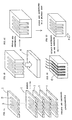
- Fig. 1 depicts one example of a multislit type actuator according to the invention.
- Fig. 1A to Fig. 1D depict the outline of manufacturing processes and
- Fig. 1E depicts the outline of the completed actuator.
- piezoelectric material green sheets 1 (hereinafter, simply called sheets) are formed with slits 2 and laminated simultaneously by a method described later.
- the sheets 1 are laminated to form comb teeth 3, and the lamination is completed at the same time when punching is finished in Fig. 1A.
- the laminated sheets 1, 1... are placed on a substrate 3 made of a sheet separately prepared, so that the comb teeth 3 are formed thereon at the same time in Fig. 1B. They are heated and compressed to closely contact each layer in Fig. 1C, and the entire sheets 1, 1- and the substrate 4 are integrated in a unitary body by firing to complete drive portions in Fig. 1D.
- electrodes 6 are formed on the wall surfaces and the like inside the slits to obtain a complete multislit type actuator in Fig. 1E.
- the sheets described above are formed by a well-known tape forming technique such as a doctor blade method and the like.
- Fig. 2 shows a concrete manufacturing method for carrying out formation and laminating of the comb teeth 3 at the same moment.
- a metal mold is used which comprises a punch 8 around which a stripper 10 for operating sheet laminating is disposed, and a die 9.
- Fig. 2A shows a before punching-out state in which a first sheet 1a is mounted on the die, and in Fig. 2B, the punch 8 and the stripper 10 are lowered and the sheet 1a is punched out slit apertures to form comb teeth (first process).
- a method for contacting the sheet 1 to the stripper 10 can be performed by forming a suction aperture in the stripper 10 to perform vacuum suction.
- the punch 8 and the stripper 10 are pulled up from the die 9. At mid-flow of the pulling-up, it is preferable that a top portion of the punch 8 is not returned to inside of the slit aperture of the first sheet 1a which was pulled up jointly.
- the top portion of the punch is stopped at a position where it is pulled in slightly from the lowest portion of the sheet 1a which was pulled up jointly (third process). If the punch 8 is returned to inside of the aperture of the first sheet 1a, or is housed completely in the stripper 10, the formed apertures are deformed since the sheet 1 is soft. Thus, flatness of a side surface is deteriorated when the sheets are laminated to form the comb teeth.
- Fig. 2D shows a process for punching out the second sheet 1b, and by closely contacting the first sheet 1a to the stripper 10, the second sheet 1b can be mounted easily on the die 9 and then punched out as shown in Fig. 2B. Further, the second sheet 1b can be overlapped on the first sheet 1a simultaneously ( fourth process).
- the first sheet 1a and the second sheet 1b which are punched out by repeating processes of Fig. 2C and Fig. 2D, are overlapped and pulled up by the stripper 10 (fifth process), and punching-out of a third sheet 1c is prepared.
- Fig. 2E shows a state where punching-out is completed.
- punching-out and laminating of sheets 1 as required are completed, holding of the sheet by the stripper 10 is released, and it becomes possible that the sheet 1 which was punched out and laminated is separated from the stripper 10, as shown in the figure.
- the separation can be surely carried out by disposing a separation jig 11 on an under surface of the stripper.
- the operation described above is one to which a manufacturing method described in Japanese Patent Application No. 2000-280573 is applied.
- a multislit type laminated body in comb teeth with desirable thickness can be obtained.
- the laminated body is disposed on the substrate 4 made of a piezoelectric material green sheet in the same manner.
- compressing and laminating process is performed to form a laminated body which is capable of handling, and then, on the condition which is suitable to characteristics of the sheet, the laminated body is fired and integrated (eighth process).
- Fig. 3A depicts an end view seen from P shown in Fig. 1D
- Fig. 3B depicts an enlarged schematic cross section of M part in the wall surface of the slit.
- the experimental results of alignment precision of stacking accuracy according to the manufacturing method described above will be shown. For example, when comb teeth having a slit of 70 ⁇ m and a width of 100 ⁇ m are formed in a sheet having a hotness of 40 ⁇ m and a Young's modulus of 39 N/mm 2 and ten layers of the sheets are laminated, an amount of an alignment deviation between the layers after fired is 4 ⁇ m at the maximum, and a surface roughness Rt is 7 ⁇ m.
- the side surfaces of the comb teeth are smoothened without convexo-concave. Since the wall surfaces of the slits are fired surfaces, transgranular fracture is not occurred in piezoelectric crystal grains even in crystal grains in the surface, and the crystal grains under transgranular fracture can be suppressed at 1% or less as shown in Fig. 3B. Additionally, the slit width after fired was about 55 ⁇ m by firing shrinkage.
- the punch and the die are used to perform the formation of the slits and lamination simultaneously, and the punch itself is also used as the positioning axis for laminating the piezoelectric material green sheets, thereby preventing the slit apertures formed by the punch from being deformed. Therefore, the deformation of the slit apertures is not occurred and an amount of an alignment deviation between the layers can be suppressed less than 5 ⁇ m. Further, the lamination having a high precision can be performed, and the wall surfaces of the slits with few convexo-concave can be formed. On this account, even the comb teeth having a slit width of less than 70 ⁇ m and a slit depth of an aspect ratio of 10 or greater can be formed easily, and an actuator having excellent properties can be obtained.
- the deterioration in the property due to compressive residual stress is not generated because the crystal grains in the wall surfaces of the slit between the comb teeth are not destroyed.
- a jig for transferring the sheets or space for lamination is unnecessary according to the manufacturing method described above, and then manufacturing lines can be simplified as well, and manufacture at low costs is feasible.
- the slit width shrinks at the time of firing which is almost the same as the punching width of the punch at the time of punching the sheet.
- the combination of machining thin slits and firing shrinkage can form micro-slits having a width of 30 to 50 ⁇ m.
- slits can be formed easily other than linear ones depending on the design of the punch, allowing the optimum shapes to be formed according to use.
- Fig. 4 depicts another manufacturing method according to the invention. Describing one by one, each of sheets 1 is formed with slit-shaped apertures 2a and laminated simultaneously applying the method described above in Fig. 4A. When punching and laminating the sheets are finished, the laminated product is similarly stacked on a substrate 4 made of a piezoelectric material green sheet in Fig. 4B. Then they are heated and compressed to closely contact each layer in Fig. 4C, and fired and integrated in a unitary body in Fig. 4D. The manufacturing method from Fig. 4A to Fig. 4D is the same as the manufacturing method shown in Fig. 2.
- the slit apertures 2a to be formed by punching are long apertures with both ends closed respectively, and are cut in one ends in Fig. 4E after being fired for forming the multislit shaped in comb teeth. Thereafter, electrodes and the like are formed for completion.
- the comb teeth are not formed by punching directly, and the both ends of the comb teeth are joined for lamination.
- the alignment precision of stacking of the comb tooth parts of each sheet can be more improved. It should be noted that cleaning to drying process for the cut parts is required to increase processes, since the end parts need to be cut after fired.
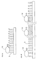
- Fig. 5 is cross sectional explanatory drawings of an actuator part being the essential part of a shear mode type head, depicting the case where the multislit type actuator according to the invention is adapted to an inkjet head.
- slits 13a and 13b having two kinds of width are alternately formed, and the slits 13a of wide width are disposed as ink chambers and the slits 13b of narrow width are disposed as slits for separation of adjacent ink chambers.
- the manufacturing method described above can easily form adjacent slits having various kinds of width. Accordingly, when the all ink chambers are separated by the slits 13b, they can be driven independently, and the shear mode type head of high performance can be obtained.
- the tip end portions of the comb teeth are formed wide in width, and slits are formed narrow in reverse.
- a shape of an ink path suitable for fluid and the shape intending the reduction in stress in the joined surface to the nozzle plate can be easily realized.
- the piezoelectric deforming stress occurred at the joined portion which is the portion of the nozzle plate (shown in Fig. 11) to be bonded to the tip end surfaces of the comb teeth can be reduced.
- the optimum slit width can be formed in accordance with the purpose to provide an actuator having the optimum property. Further, a shape suitable for fluid can be formed when the slits are used as the ink path for an inkjet head. Moreover, the piezoelectric deforming stress of the tip end portions of the comb teeth can be reduced, and long lifetime can be obtained without interposing another component.
- Fig. 6 depicts the case where the multislit type actuator according to the invention is adapted to a transfer apparatus.
- Fig. 6A depicts that slits are formed at a fixed interval to allow transfer at a constant speed
- Fig. 6B depicts that the intervals between slits are varied to change the transfer speed.
- 14 denotes a carrier part, and voltage is applied to each of the comb teeth 3 to deform them in the arrow direction, thereby allowing the placed part to be transferred as shown in Fig. 6A.
- the transfer method is a problem.
- the transfer apparatus is formed by the multislit type actuator in this manner, a micromachine can be transferred smoothly.
- the multislit type actuator according to the invention can be also utilized as a micro relay or microswitch, greatly contributing to the development of the industry.
Landscapes
- Engineering & Computer Science (AREA)
- Manufacturing & Machinery (AREA)
- Particle Formation And Scattering Control In Inkjet Printers (AREA)
Abstract
Description
Claims (9)
- A multislit type actuator characterized by comprising a plurality of piezoelectric actuators aligned and allocated in comb teeth formed on a substrate, wherein a condition of crystal grains in side surfaces of the piezoelectric actuators forming wall surfaces of a slit between the comb teeth is that the crystal grains under transgranular fracture are 1% or below.
- The multislit type actuator according to claim 1, wherein an amount of convexo-concave in the wall surfaces of the slit is 10 µm or less.
- The multislit type actuator according to claim 1, wherein a surface roughness Rt of the wall surfaces of the slit is 10 µm or less.
- The multislit type actuator according to any one of claims 1 to 3, wherein a slit width between the comb teeth is varied from a back to a tip end of the comb teeth.
- The multislit type actuator according to any one of claims 1 to 4 having slits of at least two kinds of width, wherein the slit width between each of the comb teeth is not the same.
- The multislit type actuator according to any one of claims 1 to 5, wherein a minimum slit width is less than 70 µm.
- An inkjet head driven by a shear mode, wherein a top of the actuator opposing to the substrate of the multislit type actuator according to any one of claims 1 to 6 is closed by a closing plate, and the slit is formed as an ink chamber to allow ink to be discharged in a direction of the tip of comb teeth.
- An inkjet head driven by a shear mode, wherein side surfaces of two multislit type actuators according to any one of claims 1 to 6 are joined so as to align with comb tooth parts each other, and slit portions formed in a chamber shape as ink chambers to allow ink to be discharged in a tip direction of the comb teeth.
- A method for manufacturing a multislit type actuator having a plurality of actuators each of which comprising a piezoelectric material are aligned and allocated on a substrate in comb teeth, comprising:a first process in which a plurality of piezoelectric material green sheets are prepared, and slit apertures are formed on a first piezoelectric material green sheet among the above plural piezoelectric material green sheets by use of a punch and a die;a second process in which the above first piezoelectric material green sheet is pulled up by use of a stripper;a third process in which a top portion of the above punch is pulled up to the extent that it is pulled in slightly from the lowest portion of the above pulled up first piezoelectric material green sheet;a fourth process in which second slit apertures are formed into in a second piezoelectric material green sheet by the above punch;a fifth process in which the above second piezoelectric material green sheet is pulled up jointly with the above first piezoelectric material green sheet;a sixth process in which the top portion of the above punch is pulled up to the extent that it is pulled in slightly from the lowest portion of the above pulled up second piezoelectric material green sheet;a seventh process in which hereafter a plurality of the piezoelectric material green sheets being laminated by repeating from the fourth process to the sixth process to form a plurality of piezoelectric layers of comb teeth shape; andan eighth process in which the piezoelectric layers are fired so that one side surface of the piezoelectric layers is brought into close contact with a substrate.
Applications Claiming Priority (3)
| Application Number | Priority Date | Filing Date | Title |
|---|---|---|---|
| JP2001108986 | 2001-04-06 | ||
| JP2001108986 | 2001-04-06 | ||
| PCT/JP2002/003422 WO2002084752A1 (en) | 2001-04-06 | 2002-04-05 | Multi-slit actuator, ink jet head, and method of manufacturing multi-slit actuator |
Publications (3)
| Publication Number | Publication Date |
|---|---|
| EP1389805A1 true EP1389805A1 (en) | 2004-02-18 |
| EP1389805A4 EP1389805A4 (en) | 2007-05-30 |
| EP1389805B1 EP1389805B1 (en) | 2010-11-03 |
Family
ID=18961026
Family Applications (1)
| Application Number | Title | Priority Date | Filing Date |
|---|---|---|---|
| EP20020714486 Expired - Lifetime EP1389805B1 (en) | 2001-04-06 | 2002-04-05 | Multislit type actuator, inkjet head, and method for manufacturing multislit type actuator |
Country Status (5)
| Country | Link |
|---|---|
| US (1) | US7025444B2 (en) |
| EP (1) | EP1389805B1 (en) |
| JP (1) | JP4259115B2 (en) |
| DE (1) | DE60238183D1 (en) |
| WO (1) | WO2002084752A1 (en) |
Cited By (1)
| Publication number | Priority date | Publication date | Assignee | Title |
|---|---|---|---|---|
| AT523510A1 (en) * | 2020-01-29 | 2021-08-15 | Piezocryst Advanced Sensorics | Structured, piezoelectric sensor element |
Families Citing this family (1)
| Publication number | Priority date | Publication date | Assignee | Title |
|---|---|---|---|---|
| JP2010233339A (en) * | 2009-03-26 | 2010-10-14 | Seiko Epson Corp | Piezoelectric motor, liquid ejecting apparatus and clock |
Family Cites Families (12)
| Publication number | Priority date | Publication date | Assignee | Title |
|---|---|---|---|---|
| US20057A (en) * | 1858-04-27 | Buffer-head for railroad-couplings | ||
| JPS6381003A (en) * | 1986-09-25 | 1988-04-11 | 日本電気株式会社 | Through-hole forming device |
| US4887100A (en) * | 1987-01-10 | 1989-12-12 | Am International, Inc. | Droplet deposition apparatus |
| EP0372521B1 (en) * | 1988-12-07 | 1993-04-14 | Seiko Epson Corporation | On-demand type ink jet print head |
| JPH05116329A (en) * | 1991-07-02 | 1993-05-14 | Tokyo Electric Co Ltd | Inkjet printer head manufacturing method |
| US5650810A (en) * | 1992-12-03 | 1997-07-22 | Brother Kogyo Kabushiki Kaisha | Ink jet print head having a manifold wall portion and method of producing the same by injection molding |
| JP3227285B2 (en) | 1993-09-17 | 2001-11-12 | シチズン時計株式会社 | Method of manufacturing inkjet head |
| JPH09207332A (en) * | 1996-02-05 | 1997-08-12 | Citizen Watch Co Ltd | Inkjet recording head |
| JPH11254678A (en) * | 1998-03-13 | 1999-09-21 | Kyocera Corp | Printing apparatus and manufacturing method thereof |
| JP3537700B2 (en) * | 1998-09-29 | 2004-06-14 | 京セラ株式会社 | Printing equipment |
| JP2001063048A (en) * | 1999-08-26 | 2001-03-13 | Kyocera Corp | Piezoelectric / electrostrictive film type actuator and ink jet printer head using the same |
| US6502302B2 (en) * | 2000-07-19 | 2003-01-07 | Ngk Insulators, Ltd. | Process for producing an industrial member having throughholes of high aspect ratio |
-
2002
- 2002-04-05 JP JP2002581594A patent/JP4259115B2/en not_active Expired - Fee Related
- 2002-04-05 EP EP20020714486 patent/EP1389805B1/en not_active Expired - Lifetime
- 2002-04-05 DE DE60238183T patent/DE60238183D1/en not_active Expired - Lifetime
- 2002-04-05 WO PCT/JP2002/003422 patent/WO2002084752A1/en not_active Ceased
-
2003
- 2003-10-03 US US10/679,188 patent/US7025444B2/en not_active Expired - Fee Related
Cited By (2)
| Publication number | Priority date | Publication date | Assignee | Title |
|---|---|---|---|---|
| AT523510A1 (en) * | 2020-01-29 | 2021-08-15 | Piezocryst Advanced Sensorics | Structured, piezoelectric sensor element |
| AT523510B1 (en) * | 2020-01-29 | 2021-10-15 | Piezocryst Advanced Sensorics | Structured, piezoelectric sensor element |
Also Published As
| Publication number | Publication date |
|---|---|
| US7025444B2 (en) | 2006-04-11 |
| JPWO2002084752A1 (en) | 2004-08-05 |
| EP1389805A4 (en) | 2007-05-30 |
| DE60238183D1 (en) | 2010-12-16 |
| WO2002084752A1 (en) | 2002-10-24 |
| US20040119791A1 (en) | 2004-06-24 |
| JP4259115B2 (en) | 2009-04-30 |
| EP1389805B1 (en) | 2010-11-03 |
Similar Documents
| Publication | Publication Date | Title |
|---|---|---|
| EP1375916B1 (en) | Micro pump | |
| EP1482571B1 (en) | Cell driving type piezoelectric/electrostrictive actuator and method of manufacturing the same | |
| KR960703731A (en) | Drop Deposition Apparatus and Method of Manufacturing the Same (DROPLET DEPOSITION APPARATUS AND METHOD OF MANUFACTURE) | |
| EP1270232B1 (en) | Manufacture of ink jet printheads | |
| EP1364793B1 (en) | Comb piezoelectric actuator, and its manufacturing method | |
| US6538363B2 (en) | Method of manufacturing a piezoelectric element | |
| US7468112B2 (en) | Method of producing a ceramic laminate | |
| JP3693939B2 (en) | Cell-driven micropump member and manufacturing method | |
| US7374628B2 (en) | Method for manufacturing a cell-driving-type micro pump member | |
| EP1389805B1 (en) | Multislit type actuator, inkjet head, and method for manufacturing multislit type actuator | |
| EP2267810A1 (en) | Laminated piezoelectric ceramic element fabrication method | |
| US6933663B2 (en) | Cell driving type actuator and method for manufacturing the same | |
| US20020140318A1 (en) | Matrix type actuator | |
| JP2002118303A (en) | Piezo actuator | |
| US20020195902A1 (en) | Cell driving type actuator and method for manufacturing the same | |
| KR19990012954A (en) | Manufacturing method of laminated ceramic parts |
Legal Events
| Date | Code | Title | Description |
|---|---|---|---|
| PUAI | Public reference made under article 153(3) epc to a published international application that has entered the european phase |
Free format text: ORIGINAL CODE: 0009012 |
|
| 17P | Request for examination filed |
Effective date: 20031024 |
|
| AK | Designated contracting states |
Kind code of ref document: A1 Designated state(s): AT BE CH CY DE DK ES FI FR GB GR IE IT LI LU MC NL PT SE TR |
|
| AX | Request for extension of the european patent |
Extension state: AL LT LV MK RO SI |
|
| A4 | Supplementary search report drawn up and despatched |
Effective date: 20070503 |
|
| RIC1 | Information provided on ipc code assigned before grant |
Ipc: B41J 2/16 20060101ALI20070425BHEP Ipc: H01L 41/09 20060101AFI20021029BHEP Ipc: H01L 41/24 20060101ALI20070425BHEP |
|
| 17Q | First examination report despatched |
Effective date: 20070813 |
|
| GRAP | Despatch of communication of intention to grant a patent |
Free format text: ORIGINAL CODE: EPIDOSNIGR1 |
|
| RIC1 | Information provided on ipc code assigned before grant |
Ipc: B41J 2/14 20060101ALI20100326BHEP Ipc: H01L 41/09 20060101AFI20100326BHEP Ipc: H01L 41/24 20060101ALI20100326BHEP |
|
| RTI1 | Title (correction) |
Free format text: MULTISLIT TYPE ACTUATOR, INKJET HEAD, AND METHOD FOR MANUFACTURING MULTISLIT TYPE ACTUATOR |
|
| GRAS | Grant fee paid |
Free format text: ORIGINAL CODE: EPIDOSNIGR3 |
|
| GRAA | (expected) grant |
Free format text: ORIGINAL CODE: 0009210 |
|
| AK | Designated contracting states |
Kind code of ref document: B1 Designated state(s): DE GB |
|
| REG | Reference to a national code |
Ref country code: GB Ref legal event code: FG4D |
|
| REF | Corresponds to: |
Ref document number: 60238183 Country of ref document: DE Date of ref document: 20101216 Kind code of ref document: P |
|
| PLBE | No opposition filed within time limit |
Free format text: ORIGINAL CODE: 0009261 |
|
| STAA | Information on the status of an ep patent application or granted ep patent |
Free format text: STATUS: NO OPPOSITION FILED WITHIN TIME LIMIT |
|
| 26N | No opposition filed |
Effective date: 20110804 |
|
| REG | Reference to a national code |
Ref country code: DE Ref legal event code: R097 Ref document number: 60238183 Country of ref document: DE Effective date: 20110804 |
|
| PGFP | Annual fee paid to national office [announced via postgrant information from national office to epo] |
Ref country code: GB Payment date: 20120327 Year of fee payment: 11 |
|
| PGFP | Annual fee paid to national office [announced via postgrant information from national office to epo] |
Ref country code: DE Payment date: 20120430 Year of fee payment: 11 |
|
| REG | Reference to a national code |
Ref country code: DE Ref legal event code: R119 Ref document number: 60238183 Country of ref document: DE |
|
| GBPC | Gb: european patent ceased through non-payment of renewal fee |
Effective date: 20130405 |
|
| PG25 | Lapsed in a contracting state [announced via postgrant information from national office to epo] |
Ref country code: GB Free format text: LAPSE BECAUSE OF NON-PAYMENT OF DUE FEES Effective date: 20130405 Ref country code: DE Free format text: LAPSE BECAUSE OF NON-PAYMENT OF DUE FEES Effective date: 20131101 |
|
| REG | Reference to a national code |
Ref country code: DE Ref legal event code: R079 Ref document number: 60238183 Country of ref document: DE Free format text: PREVIOUS MAIN CLASS: H01L0041090000 Ipc: H01L0041053000 |
|
| REG | Reference to a national code |
Ref country code: DE Ref legal event code: R119 Ref document number: 60238183 Country of ref document: DE Effective date: 20131101 Ref country code: DE Ref legal event code: R079 Ref document number: 60238183 Country of ref document: DE Free format text: PREVIOUS MAIN CLASS: H01L0041090000 Ipc: H01L0041053000 Effective date: 20141105 |