EP1389747A2 - Lithographic projection apparatus and reflector asembly for use in said apparatus - Google Patents
Lithographic projection apparatus and reflector asembly for use in said apparatus Download PDFInfo
- Publication number
- EP1389747A2 EP1389747A2 EP03077572A EP03077572A EP1389747A2 EP 1389747 A2 EP1389747 A2 EP 1389747A2 EP 03077572 A EP03077572 A EP 03077572A EP 03077572 A EP03077572 A EP 03077572A EP 1389747 A2 EP1389747 A2 EP 1389747A2
- Authority
- EP
- European Patent Office
- Prior art keywords
- radiation
- reflector
- source
- optical axis
- reflectors
- Prior art date
- Legal status (The legal status is an assumption and is not a legal conclusion. Google has not performed a legal analysis and makes no representation as to the accuracy of the status listed.)
- Granted
Links
Images



Classifications
-
- B—PERFORMING OPERATIONS; TRANSPORTING
- B82—NANOTECHNOLOGY
- B82Y—SPECIFIC USES OR APPLICATIONS OF NANOSTRUCTURES; MEASUREMENT OR ANALYSIS OF NANOSTRUCTURES; MANUFACTURE OR TREATMENT OF NANOSTRUCTURES
- B82Y10/00—Nanotechnology for information processing, storage or transmission, e.g. quantum computing or single electron logic
-
- G—PHYSICS
- G03—PHOTOGRAPHY; CINEMATOGRAPHY; ANALOGOUS TECHNIQUES USING WAVES OTHER THAN OPTICAL WAVES; ELECTROGRAPHY; HOLOGRAPHY
- G03F—PHOTOMECHANICAL PRODUCTION OF TEXTURED OR PATTERNED SURFACES, e.g. FOR PRINTING, FOR PROCESSING OF SEMICONDUCTOR DEVICES; MATERIALS THEREFOR; ORIGINALS THEREFOR; APPARATUS SPECIALLY ADAPTED THEREFOR
- G03F7/00—Photomechanical, e.g. photolithographic, production of textured or patterned surfaces, e.g. printing surfaces; Materials therefor, e.g. comprising photoresists; Apparatus specially adapted therefor
- G03F7/70—Microphotolithographic exposure; Apparatus therefor
- G03F7/70058—Mask illumination systems
- G03F7/7015—Details of optical elements
- G03F7/70166—Capillary or channel elements, e.g. nested extreme ultraviolet [EUV] mirrors or shells, optical fibers or light guides
-
- G—PHYSICS
- G03—PHOTOGRAPHY; CINEMATOGRAPHY; ANALOGOUS TECHNIQUES USING WAVES OTHER THAN OPTICAL WAVES; ELECTROGRAPHY; HOLOGRAPHY
- G03F—PHOTOMECHANICAL PRODUCTION OF TEXTURED OR PATTERNED SURFACES, e.g. FOR PRINTING, FOR PROCESSING OF SEMICONDUCTOR DEVICES; MATERIALS THEREFOR; ORIGINALS THEREFOR; APPARATUS SPECIALLY ADAPTED THEREFOR
- G03F7/00—Photomechanical, e.g. photolithographic, production of textured or patterned surfaces, e.g. printing surfaces; Materials therefor, e.g. comprising photoresists; Apparatus specially adapted therefor
- G03F7/70—Microphotolithographic exposure; Apparatus therefor
- G03F7/708—Construction of apparatus, e.g. environment aspects, hygiene aspects or materials
- G03F7/70908—Hygiene, e.g. preventing apparatus pollution, mitigating effect of pollution or removing pollutants from apparatus
- G03F7/70916—Pollution mitigation, i.e. mitigating effect of contamination or debris, e.g. foil traps
Definitions
- the invention relates to a lithographic projection apparatus comprising:
- Lithographic projection apparatus can be used, for example, in the manufacture of integrated circuits (ICs).
- the patterning means may generate a circuit pattern corresponding to an individual layer of the IC, and this pattern can be imaged onto a target portion (e.g. comprising one or more dies) on a substrate (silicon wafer) that has been coated with a layer of radiation-sensitive material (resist).
- a target portion e.g. comprising one or more dies
- a substrate silicon wafer
- a layer of radiation-sensitive material resist
- a single wafer will contain a whole network of adjacent target portions that are successively irradiated via the projection system, one at a time.
- employing patterning by a mask on a mask table a distinction can be made between two different types of machine.
- each target portion is irradiated by exposing the entire mask pattern onto the target portion in one go: such an apparatus is commonly referred to as a wafer stepper or step-and-repeat apparatus.
- an alternative apparatus commonly referred to as a step-and-scan apparatus ⁇ each target portion is irradiated by progressively scanning the mask pattern under the projection beam in a given reference direction (the "scanning" direction) while synchronously scanning the substrate table parallel or anti-parallel to this direction; since, in general, the projection system will have a magnification factor M (generally ⁇ 1), the speed V at which the substrate table is scanned will be a factor M times that at which the mask table is scanned.
- M magnification factor
- a pattern (e.g. in a mask) is imaged onto a substrate that is at least partially covered by a layer of radiation-sensitive material (resist).
- the substrate Prior to this imaging step, the substrate may undergo various procedures, such as priming, resist coating and a soft bake. After exposure, the substrate may be subjected to other procedures, such as a post-exposure bake (PEB), development, a hard bake and measurement/inspection of the imaged features.
- PEB post-exposure bake
- This array of procedures is used as a basis to pattern an individual layer of a device, e.g. an IC.
- Such a patterned layer may then undergo various processes such as etching, ion-implantation (doping), metallization, oxidation, chemo-mechanical polishing, etc., all intended to finish off an individual layer. If several layers are required, then the whole procedure, or a variant thereof, will have to be repeated for each new layer. Eventually, an array of devices will be present on the substrate (wafer). These devices are then separated from one another by a technique such as dicing or sawing, whence the individual devices can be mounted on a carrier, connected to pins, etc.
- the projection system may hereinafter be referred to as the "lens"; however, this term should be broadly interpreted as encompassing various types of projection system, including refractive optics, reflective optics, and catadioptric systems, for example.
- the radiation system may also include components operating according to any of these design types for directing, shaping or controlling the projection beam of radiation, and such components may also be referred to below, collectively or singularly, as a "lens".
- the lithographic apparatus may be of a type having two or more substrate tables (and/or two or more mask tables). In such "multiple stage” devices the additional tables may be used in parallel, or preparatory steps may be carried out on one or more tables while one or more other tables are being used for exposures. Dual stage lithographic apparatus are described, for example, in US 5,969,441 and WO 98/40791, both incorporated herein by reference.
- lithographic projection apparatus In a lithographic apparatus the size of features that can be imagined onto the substrate is limited by the wavelength of the projection radiation. To produce integrated circuits with a higher density of devices, and hence higher operating speeds, it is desirable to be able to image smaller features. Whilst most current lithographic projection apparatus employ ultraviolet light generated by mercury lamps or excimer lasers, it has been proposed to use shorter wavelength radiation in the range 5 to 20 nm, especially around 13 nm. Such radiation is termed extreme ultraviolet (EUV) or soft x-ray and possible sources include, for instance, laser-produced plasma sources, discharge plasma sources, or synchrotron radiation from electron storage rings. Apparatus using discharge plasma sources are described in: W. Partlo, I. Fomenkov, R. Oliver, D.
- EUV extreme ultraviolet
- EUV radiation sources may require the use of a rather high partial pressure of a gas or vapor to emit EUV radiation, such as discharge plasma radiation sources referred to above.
- a discharge plasma source for instance, a discharge is created in between electrodes, and a resulting partially ionized plasma may subsequently be caused to collapse to yield a very hot plasma that emits radiation in the EUV range.
- the very hot plasma is quite often created in Xe, since a Xe plasma radiates in the Extreme UV (EUV) range around 13.5 nm.
- EUV Extreme UV
- a typical pressure of 0.1 mbar is required near the electrodes to the radiation source.
- a drawback of having such a rather high Xe pressure is that Xe gas absorbs EUV radiation.
- 0.1 mbar Xe transmits over 1 m only 0.3 % EUV radiation having a wavelength of 13.5 nm. It is therefore required to confine the rather high Xe pressure to a limited region around the source.
- the source can be contained in its own vacuum chamber that is separated by a chamber wall from a subsequent vacuum chamber in which the collector mirror and illumination optics may be obtained.
- the pressure in the optical system of the illuminator is maintained relatively low, for instance at 1/1000 of the pressure of the radiation source, which may comprise Xe at a source pressure of 0.1 mbar.
- European patent applications EP-A-1 233 468 and EP-A-1 057 079 propose a so called foil trap structure in proximity to the source to block debris and/or to generate a pressure drop between a source chamber and an optics chamber without substantially blocking the EUV radiation path.
- the optical elements in proximity to the source need to be supported in the EUV radiation beam using support structures at a position that prevents significant obstruction of the EUV projection beam.
- a reflector assembly for reflecting electromagnetic radiation, the reflector assembly comprising at least a first reflector and a second reflector, said first reflector and said second reflector extending in the direction of an optical axis, having a reflective surface and a backing surface, in which assembly an imaginary line perpendicular to the optical axis intersecting said reflectors, intersects said first reflector at a first distance from the optical axis and intersects said second reflector at a second distance from the optical axis, the first distance being larger than the second distance, rays deriving from a point on the optical axis being cut off by second reflector and being reflected on the reflective surface of the first reflector defining zones of high radiation intensity and zones of low radiation intensity between said reflectors, characterized in that a structure is present on the backing surface of the second reflector at the position of the low intensity zone.
- the reflector assembly functions as a collector of EUV radiation emitted by the source and directs a collimated beam of EUV radiation focused in the intermediate focus to further optical components along an optical axis to form the projection beam.
- a specific spatial segment of the projection beam with the source as a center, is intercepted.
- the radiation propagates by being reflected at grazing angles off the reflective surface of the upper reflector.
- the space occupied by the reflected rays between the reflectors is defined by the rays emanating from the source and being intercepted by the entry parts of the reflectors.
- These rays bound zones generally being rotionally symmetric around the optical axis of low radiation intensity in which the structural objects of the present invention are placed, preferably supported on the backing surface of the reflector closest to the optical axis.
- the invention also relates to a reflector assembly for reflecting electromagnetic radiation, the reflector assembly comprising at least a first reflector and a second reflector, said first reflector and said second reflector extending in the direction of an optical axis, having a reflective surface and a backing surface, in which assembly an imaginary line perpendicular to the optical axis intersecting said reflectors, intersects said first reflector at a first distance from the optical axis and intersects said second reflector at a second distance from the optical axis, the first distance being larger than the second distance, rays deriving from a point on the optical axis being cut off by second reflector and being reflected on the reflective surface of the first reflector defining zones of high radiation intensity and zones of low radiation intensity between said reflectors, characterized in that at least one of a nozzle for directing a fluid in the reflectors; a gas barrier member for increasing a fluid resistance of fluid passing between the reflectors; heat transfer means; and a transducer member for forming a signal and
- the reflectors extend at an angle to the optical axis.
- Each reflector may comprise at least two adjacent reflecting surfaces, the reflecting surfaces further from the source being placed at the smaller angle to the optical axis than the reflecting surface is closer to the source.
- a grazing incidence collector may be constructed for generating a beam of EUV radiation propagating along the optical axis.
- at least two reflectors are placed substantially coaxially and extend substantially rotationally symmetric around the optical axis.
- a grazing incidence collector of this (Wolter-) type is, for instance, described in German patent application no. DE 101 38 284.7, which is incorporated herein by reference.
- said nozzle comprises at least one fluid supply means for directing a fluid in the direction of the source.
- a buffer gas at relatively high pressure and low gas volume can be directed towards the source for removal of debris emitted by the source.
- a high pressure and low gas load can be obtained.
- the gas used is substantially transparent to EUV radiation and may be formed of He, Ar, N 2 , H 2 .
- a fluid removal unit such as a pump, may be situated for removal of the gas and for preventing the gas from reaching the EUV source.
- the reflectors may be placed in a chamber having an opening comprising a pressure reduction member, such as a foil trap referred to earlier, the radiation source being placed in an adjacent source housing and emitting radiation through the pressure reduction member, the fluid removal unit being located in the chamber for removing fluid near the pressure reduction member, a second fluid removal unit being connected to the source housing.
- a pressure reduction member such as a foil trap referred to earlier
- the flow resistance of the reflector assembly is increased by placing a gas barrier member in the low intensity regions.
- the reflector assembly may form an effective vacuum separation between a source side and the optical components downstream of the optical axis, allowing removal of gas at a downstream side at relatively low pumping rates.
- the gas barrier may be formed by plate-shaped members that may be placed perpendicular to the backing surface of the reflector within the low intensity regions for increasing pressure resistance across the reflector along the optical axis. Pressure reduction may also be achieved by placing a barrier in the low intensity regions having a cross-section substantially corresponding to the boundaries of the low intensity zone. In this way, the gas flow rate through the collector can be reduced by approximately a factor of 2.
- the structure within the low intensity zones comprises heat transfer means, such as fluid ducts or heat-conducting elements, such as copper wires.
- the ducts or copper wires may be guided away from the reflectors through the low intensity regions and be connected to a heat exchange element at the distance from the optical axis, such as an adjustable heat sink.
- a differential heating or cooling along the optical axis may be achieved.
- transducers may be included within the low intensity regions for generating measurement signals, such as thermocouples, pressure sensors, or other structures, without affecting the EUV intensity of the generated beam.
- the invention also relates to a method of manufacturing an integrated structure by a lithographic process comprising the steps of:
- UV radiation e.g. with a wavelength of 365, 248, 193, 157 or 126 nm
- EUV extreme ultra-violet
- particle beams such as ion beams or electron beams.
- Fig. 1 schematically depicts a lithographic projection apparatus 1 according to a particular embodiment of the invention.
- the apparatus comprises:
- the source LA (e.g. a laser-produced plasma or a discharge plasma EUV radiation source) produces a beam of radiation.
- This beam is fed into an illumination system (illuminator) IL, either directly or after having traversed conditioning means, such as a beam expander Ex, for example.
- the illuminator IL may comprise adjusting means AM for setting the outer and/or inner radial extent (commonly referred to as ⁇ -outer and ⁇ -inner, respectively) of the intensity distribution in the beam,
- ⁇ -outer and ⁇ -inner respectively
- the beam PB impinging on the mask MA has a desired uniformity and intensity distribution in its cross-section.
- the source LA may be within the housing of the lithographic projection apparatus (as is often the case when the source LA is a mercury lamp, for example), but that it may also be remote from the lithographic projection apparatus, the radiation beam which it produces being led into the apparatus (e.g. with the aid of suitable directing mirrors); this latter scenario is often the case when the source LA is an excimer laser.
- the current invention and claims encompass both of these scenarios.
- the beam PB subsequently intercepts the mask MA, which is held on a mask table MT. Having traversed the mask MA, the beam PB passes through the lens PL, which focuses the beam PB onto a target portion C of the substrate W. With the aid of the second positioning means PW (and interferometric measuring means IF), the substrate table WT can be moved accurately, e.g. so as to position different target portions C in the path of the beam PB. Similarly, the first positioning means PM can be used to accurately position the mask MA with respect to the path of the beam PB, e.g. after mechanical retrieval of the mask MA from a mask library, or during a scan.
- the mask table MT may just be connected to a short stroke actuator, or may be fixed.
- Mask MA and substrate W may be aligned using mask alignment marks M1, M2 and substrate alignment marks P1, P2.
- the depicted apparatus can be used in two different modes:
- Fig. 2 shows the projection apparatus 1 comprising an illumination system IL with radiation unit 3, illumination optics unit 4, and projection optics system PL.
- the radiation system 2 comprises a source-collector module or radiation unit 3 and an illumination optics unit 4.
- Radiation unit 3 is provided with a radiation source LA which may be formed by a discharge plasma.
- EUV radiation source 6 may employ a gas or vapor, such as Xe gas or Li vapor in which a very hot plasma may be created to emit radiation in the EUV range of the electromagnetic spectrum.
- the very hot plasma is created by causing a partially ionized plasma of an electrical discharge to collapse onto the optical axis O.
- Partial pressures of 0.1 mbar of Xe, Li vapor or any other suitable gas or vapor may be required for efficient generation of the radiation.
- the radiation emitted by radiation source LA is passed from the source chamber 7 into collector chamber 8 via a gas barrier structure or "foil trap" 9.
- the gas barrier structure comprises a channel structure such as, for instance, described in detail in European patent applications EP-A-1 233 468 and EP-A-1 057 079, which is incorporated herein by reference.
- the collector chamber 8 comprises a radiation collector 10 which according to the present invention is formed by a grazing incidence collector. Radiation passed by collector 10 is reflected off a grating spectral filter 11 to be focused in a virtual source point 12 at an aperture in the collector chamber 8. From chamber 8, the projection beam 16 is reflected in illumination optics unit 4 via normal incidence reflectors 13, 14 onto a reticle or mask positioned on reticle or mask table MT. A patterned beam 17 is formed which is imaged in projection optics system PL via reflective elements 18, 19 onto wafer stage or substrate table WT. More elements than shown may generally be present in illumination optics unit 4 and projection system PL.
- the grazing incidence collector 10 comprises a number of nested reflector elements 21, 22, 23.
- a grazing incidence collector of this type is, for instance, shown in German patent application DE 101 38 284.7,
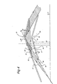
- each reflector comprises a backing surface 24, 25 and a reflective surface 26, 27.
- Reflector 22 is located at a distance r1 from the optical axis, which is generally smaller than the distance r2 from the optical axis of reflector 21.
- the distances r1 and r2 may for instance comprise 20 respectively 80 mm.
- the reflectors 21 ,22 are under an angle ⁇ respectively ⁇ with the optical axis O at r1 and r2 resprctively.
- the reflectors 21, 22 may be curved i.e.
- the angles ⁇ and ⁇ with respect to the optical axis O may vary along the optical axis O.
- Rays of radiation b1 and b2 emitted from the source 6 and being reflected by entry sections 29, 30 of reflectors 21, 22 are reflected off reflective surface 26 of top reflector 21 and define zones zh of radiation intensity in the space between reflectors 21, 22 and zones z1 of low or zero radiation intensity.
- Zones z1 are of substantial triangular cross-section and are substantially free of radiation. This allows structures 31, such as explained in detail hereafter, to be attached to backing surface 25 of reflector 22 such as to be situated in the space between reflectors 21, 22 without causing substantial absorption of radiation.
- the backing surfaces 24, 25 may be absorptive for radiation or, if so desired, reflective.
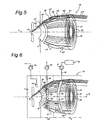
- Fig. 5 shows a perspective view of a grazing incidence reflector 10 comprising eight coaxially nested reflectors.
- Each reflector 21,22 may comprise a first reflector surface 32 and second reflector surface 33 at an angle to reflecting surface 32. Also, there may be a smooth transition from first reflecting surface 32 to second reflecting surface 33.
- Incoming ray b1 is reflected off reflector 32 as ray b'1 and reflected off reflector 33 as ray b''1.
- Incoming ray b2 is reflected off reflector 32 as reflected ray b2, rays b"1 and b2 leaving the collector and forming an annular radiation beam situated around optical axis O.
- Rays b2 and b'1 form boundary rays of first low radiation intensity zone z11, whereas reflected ray b'1 and b'2 form boundary rays of second low intensity zone z12.
- Low intensity zones z11, z12 are rotationally symmetric about optical axis O.
- the shaded area in Fig. 5 defines the high radiation intensity zones between reflectors 21, 22.
- Fig. 6 shows an embodiment wherein the grazing incidence collector 10 in the low intensity zones z11, z12 is provided with gas injection members 35, 36.
- Gas injection members may be tubes placed on the backing surfaces of the reflectors which tubes comprise openings or nozzles 37, 38 for supplying a gas in the space between adjacent reflectors in the direction of the source 6.
- the gas may be introduced into the tubes 35, 36 from a gas supply reservoir 39, via fluid duct 40 and pumping unit 41.
- the gas comprises preferably an EUV transparent gas such as He, Ar, N 2 , H 2 which is supplied at a gas flow rate in between 0 an 1000 mbar*litres/second.
- the gas stream will be substantially blocked by the foil trap 9 and will travel along the surface thereof in the directions of the arrow as indicated, and may be removed via a gas removal duct 42 and exhaust pump 43. Particles and other impurities deriving from the source 6 and travelling through the foil trap 9 will be removed by the gas stream via gas removal duct 42 without being able to travel through grazing incidence collector 10 into the projection optics unit 5. Hence, damage to projection optics can be strongly reduced.
- a gas flow at a rate in between 0 an 1000 mbar*litres/second removal can be achieved while maintaining the gas flow into the source 6 at a low level.
- a second gas removal duct 44 may be placed within source chamber 7 for removing any residual gas flow deriving from gas injection members 35, 36 at the back of foil trap 9 via exhaust pump 45.
- Fig. 7 shows an embodiment of grazing incidence collector 10 in which gas barrier members 50, 51 or 52, 53 are connected to the backing surface of the inner reflectors in low intensity zones z11, z12
- the gas barrier members 50, 51 are indicated to be formed of annular, plate-shaped members substantially perpendicular to the reflectors and extending to substantially halfway the distance between adjacent reflectors, i.e. to the top of low intensity zones z11, z12
- the gas barrier members 52, 53 are shown to be comprised of three dimensional ring-shaped gas barrier members with triangular cross-section for providing even more effective blocking of a gas flow along the reflectors towards the projection optics.
- a high pressure difference between source chamber 7 and illuminator optics chamber parts 8' can be effected, the pressure in source chamber 7 being for instance 0.1 mbar whereas pressure in illuminator optics chamber 8' are 0.001 mbar.
- a partitioning wall 54 sealingly closes off chamber 8' from illuminator optics chamber 8 such that a pressure difference between chambers 8' and 8, in view of the barrier means 50-53 may be increased.
- a xenon pressure lower than 10 -3 mbar in the illuminator optics chamber 8 is desirable.
- a xenon pressure in this range leads to a transmission higher than 94% for 13.5 nm radiation.
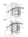
- Fig. 8 shows a grazing incidence collector 10 in which in the zones of low radiation intensity z11, z12 coaxial with the optical axis, cooling tubes 60, 61 are placed supported on the backing surface of the reflectors.
- cooling tubes 60, 61 a cooling fluid is circulated in a heat exchange loop 62, 63 placed outside the illuminator optics chamber 8. After passing heat exchangers 64, 65 the cooling fluid is recirculated, Typically, more than 250 Watt of radiation generated by the source 6 will be absorbed by the grazing incidence collector 10.
- Temperatures of the reflector of grazing incidence collector 10 near the source 6 may rise to over 100-300 °C at a position near the radiation source 6 and to temperatures ranging from 50-150 °C at a position of the collector 10 at the distance from the source 6. By cooling the collector 10, temperatures may be reduced. By proper cooling, the temperature of the collector can reach the ambient temperature level.
- a cooling fluid water may be used or a liquid metal such as Na.
- a number of cooling wires 70, 71 is placed on the backing surface of the reflectors.
- the wires may for instance be formed by copper wires.
- the cooling capacities of the wires 70 may be relatively large by placing the wires in close proximity along the optical axis O.
- the cooling wires 71 may be spaced apart further to reduce the cooling properties in order to generate a cooling gradient along the optical axis.
- the diameters of the cooling wires 70, 71 may vary.
- the end of wires 70, 71 may be connected to a heat sink 72, 72', 73.
- the heat sink may be varied in cooling capacity in order to regulate the temperature of the reflectors in dependence on the power of the source.
- a measuring unit 74 may be placed in zone of low radiation intensity z12 for supplying a measurement signal to a computing unit 75.
- Measuring unit 74 may for instance be thermocouple, such that for instance control of the radiation source 6, dependent on the temperature may occur via computing unit 75.
- a displacement unit can be employed, such as a piezo electric crystal for adjusting the position of the reflectors via computing unit 75 for instance in dependence on the power of the source 6 or the temperature of the reflectors.
- FIG. 10 shows collector support members 76,76' carrying support rods 77,78 extending through the zones of low radiation intensity z11, z12. Individual reflectors are supported on the rod 77,78 and are fixed in a accurately defined mutual relationship.
- the collectors are attached to the support rods 77, 78 in attachment points 79, 80 by appropriate attachment techniques such as welding or brazing.
- the reflectors together with the support rods 77, 78 form, when viewed parallel to the optical axis O, a "spider wheel” structure. This structure creates a shade in the rest of the system (downstream of the structure). Upstream of the "spider wheel” structure, objects can be placed in the (virtual) shade of the structure. These object will be radiated by the EUV beam. However, this will not result in less light downstream of the structure.
- the collector 10 there are low-intensity zones, and additional zones which correspond to the upstream shade of the structure. Both zones can be used for the purposes as described above. Since the upstream shades of the structure extend outside the collector, they can be used for gas inlet, cable input/output and additional support structure for transducers, gas nozzles, pumping restrictions and cooling structures.
Landscapes
- Engineering & Computer Science (AREA)
- Physics & Mathematics (AREA)
- Chemical & Material Sciences (AREA)
- General Physics & Mathematics (AREA)
- Life Sciences & Earth Sciences (AREA)
- Atmospheric Sciences (AREA)
- Health & Medical Sciences (AREA)
- Epidemiology (AREA)
- Public Health (AREA)
- Nanotechnology (AREA)
- Environmental & Geological Engineering (AREA)
- Theoretical Computer Science (AREA)
- Crystallography & Structural Chemistry (AREA)
- Mathematical Physics (AREA)
- Exposure Of Semiconductors, Excluding Electron Or Ion Beam Exposure (AREA)
- Exposure And Positioning Against Photoresist Photosensitive Materials (AREA)
Abstract
Description
- an illumination system with a radiation source, to form a projection beam of radiation,
- a support structure constructed to hold patterning means, to be irradiated by the projection beam to pattern said projection beam,
- a substrate table constructed to hold a substrate, and
- a projection system constructed and arranged to image an irradiated portion of the patterning means onto a target portion of the substrate. The term "patterning means" as here employed should be broadly interpreted as referring to means that can be used to endow an incoming radiation beam with a patterned cross-section, corresponding to a pattern that is to be created in a target portion of the substrate; the term "light valve" can also be used in this context. Generally, the said pattern will correspond to a particular functional layer in a device being created in the target portion, such as an integrated circuit or other device (see below). Examples of such patterning means include;
- A mask. The concept of a mask is well known in lithography, and it includes mask types such as binary, alternating phase-shift, and attenuated phase-shift, as well as various hybrid mask types. Placement of such a mask in the radiation beam causes selective transmission (in the case of a transmissive mask) or reflection (in the case of a reflective mask) of the radiation impinging on the mask, according to the pattern on the mask. In the case of a mask, the support structure will generally be a mask table, which ensures that the mask can be held at a desired position in the incoming radiation beam, and that it can be moved relative to the beam if so desired;
- A programmable mirror array. One example of such a device is a matrix-addressable surface having a viscoelastic control layer and a reflective surface. The basic principle behind such an apparatus is that (for example) addressed areas of the reflective surface reflect incident light as diffracted light, whereas unaddressed areas reflect incident light as undiffracted light. Using an appropriate filter, the said undiffracted light can be filtered out of the reflected beam, leaving only the diffracted light behind; in this manner, the beam becomes patterned according to the addressing pattern of the matrix-adressable surface. An alternative embodiment of a programmable mirror array employs a matrix arrangement of tiny mirrors, each of which can be individually tilted about an axis by applying a suitable localized electric field, or by employing piezoelectric actuation means. Once again, the mirrors are matrix-addressable, such that addressed mirrors will reflect an incoming radiation beam in a different direction to unaddressed mirrors; in this manner, the reflected beam is patterned according to the addressing pattern of the matrix-adressable mirrors. The required matrix addressing can be performed using suitable electronic means. In both of the situations described hereabove, the patterning means can comprise one or more programmable mirror arrays. More information on mirror arrays as here referred to can be gleaned, for example, from United States Patents US 5,296,891 and US 5,523,193, and PCT patent applications WO 98/38597 and WO 98/33096, which are incorporated herein by reference. In the case of a programmable mirror array, the said support structure may be embodied as a frame or table, for example, which may be fixed or movable as required; and
- A programmable LCD array. An example of such a construction is given in United States Patent US 5,229,872, which is incorporated herein by reference. As above, the support structure in this case may be embodied as a frame or table, for example, which may be fixed or movable as required. For purposes of simplicity, the rest of this text may, at certain locations, specifically direct itself to examples involving a mask and mask table; however, the general principles discussed in such instances should be seen in the broader context of the patterning means as hereabove set forth.
These types of structures have proven to be particularly advantageous, as will be elaborated below in connection with some embodiments of the invention. In one embodiment, the reflectors extend at an angle to the optical axis. Each reflector may comprise at least two adjacent reflecting surfaces, the reflecting surfaces further from the source being placed at the smaller angle to the optical axis than the reflecting surface is closer to the source. In this way, a grazing incidence collector may be constructed for generating a beam of EUV radiation propagating along the optical axis. Preferably, at least two reflectors are placed substantially coaxially and extend substantially rotationally symmetric around the optical axis. A grazing incidence collector of this (Wolter-) type is, for instance, described in German patent application no. DE 101 38 284.7, which is incorporated herein by reference.
- providing a radiation system to form a projection beam of radiation, from radiation emitted by a radiation source,
- providing a support structure constructed to hold patterning means, to be irradiated by the projection beam to pattern said projection beam,
- providing a substrate table constructed to hold a substrate, and
- providing a projection system constructed and arranged to image an irradiated portion of the patterning means onto a target portion of the substrate,
- placing a structure in a low radiation intensive region behind the aperture
- a radiation system Ex, IL, for supplying a projection beam PB of radiation (e.g. EUV radiation) with a wavelength of 11-14 nm. In this particular case, the radiation system also comprises a radiation source LA;
- a first object table (mask table) MT provided with a mask holder for holding a mask MA (e.g. a reticle), and connected to first positioning means PM for accurately positioning the mask with respect to item PL;
- a second object table (substrate table) WT provided with a substrate holder for holding a substrate W (e.g. a resist-coated silicon wafer), and connected to second positioning means PW for accurately positioning the substrate with respect to item PL; and
- a projection system ("lens") PL for imaging an irradiated portion of the mask MA onto a target portion C (e.g. comprising one or more dies) of the substrate W. As here depicted, the apparatus is of a transmissive type (i.e. has a transmissive mask). However, in general, it may also be of a reflective type, for example (with a reflective mask). Alternatively, the apparatus may employ another kind of patterning means, such as a programmable mirror array of a type as referred to above
Claims (18)
Priority Applications (1)
| Application Number | Priority Date | Filing Date | Title |
|---|---|---|---|
| EP03077572A EP1389747B1 (en) | 2002-08-15 | 2003-08-15 | Lithographic projection apparatus and reflector asembly for use in said apparatus |
Applications Claiming Priority (3)
| Application Number | Priority Date | Filing Date | Title |
|---|---|---|---|
| EP02078390 | 2002-08-15 | ||
| EP02078390 | 2002-08-15 | ||
| EP03077572A EP1389747B1 (en) | 2002-08-15 | 2003-08-15 | Lithographic projection apparatus and reflector asembly for use in said apparatus |
Publications (3)
| Publication Number | Publication Date |
|---|---|
| EP1389747A2 true EP1389747A2 (en) | 2004-02-18 |
| EP1389747A3 EP1389747A3 (en) | 2004-04-14 |
| EP1389747B1 EP1389747B1 (en) | 2008-10-15 |
Family
ID=30771961
Family Applications (1)
| Application Number | Title | Priority Date | Filing Date |
|---|---|---|---|
| EP03077572A Expired - Lifetime EP1389747B1 (en) | 2002-08-15 | 2003-08-15 | Lithographic projection apparatus and reflector asembly for use in said apparatus |
Country Status (1)
| Country | Link |
|---|---|
| EP (1) | EP1389747B1 (en) |
Cited By (7)
| Publication number | Priority date | Publication date | Assignee | Title |
|---|---|---|---|---|
| EP1674932A1 (en) * | 2004-12-27 | 2006-06-28 | ASML Netherlands B.V. | Lithographic apparatus, illumination system and debris trapping system |
| EP1708032A3 (en) * | 2005-03-29 | 2007-01-03 | ASML Netherlands B.V. | Lithographic device, device manufacturing method and device manufactured thereby |
| EP1742110A3 (en) * | 2005-07-06 | 2007-05-23 | ASML Netherlands BV | Lithographic apparatus, contaminant trap, and device manufacturing method |
| US7502095B2 (en) | 2005-03-29 | 2009-03-10 | Asml Netherlands B.V. | Lithographic apparatus, device manufacturing method, and device manufactured thereby |
| US7910900B2 (en) | 2006-07-20 | 2011-03-22 | Carl Zeiss Smt Gmbh | Collector for an illumination system |
| NL2008216A (en) * | 2011-02-17 | 2012-08-20 | Media Lario Srl | Thermal management systems, assemblies and methods for grazing incidence collectors for euv lithography. |
| US9658542B2 (en) | 2013-10-14 | 2017-05-23 | Carl Zeiss Smt Gmbh | Optical element |
Family Cites Families (4)
| Publication number | Priority date | Publication date | Assignee | Title |
|---|---|---|---|---|
| US6064072A (en) * | 1997-05-12 | 2000-05-16 | Cymer, Inc. | Plasma focus high energy photon source |
| DE10138313A1 (en) * | 2001-01-23 | 2002-07-25 | Zeiss Carl | Collector for lighting systems with a wavelength <193 nm |
| US6285737B1 (en) * | 2000-01-21 | 2001-09-04 | Euv Llc | Condenser for extreme-UV lithography with discharge source |
| IT1316249B1 (en) * | 2000-12-01 | 2003-04-03 | Enea Ente Nuove Tec | PROCEDURE FOR THE REDUCTION OF ION FLOW AND SMALL DETRITATION IN SOFT X-RAY SOURCES FROM PLASMA, THROUGH THE USE OF KRIPTON. |
-
2003
- 2003-08-15 EP EP03077572A patent/EP1389747B1/en not_active Expired - Lifetime
Cited By (11)
| Publication number | Priority date | Publication date | Assignee | Title |
|---|---|---|---|---|
| EP1674932A1 (en) * | 2004-12-27 | 2006-06-28 | ASML Netherlands B.V. | Lithographic apparatus, illumination system and debris trapping system |
| US7145132B2 (en) | 2004-12-27 | 2006-12-05 | Asml Netherlands B.V. | Lithographic apparatus, illumination system and debris trapping system |
| EP1708032A3 (en) * | 2005-03-29 | 2007-01-03 | ASML Netherlands B.V. | Lithographic device, device manufacturing method and device manufactured thereby |
| US7502095B2 (en) | 2005-03-29 | 2009-03-10 | Asml Netherlands B.V. | Lithographic apparatus, device manufacturing method, and device manufactured thereby |
| US7684012B2 (en) | 2005-03-29 | 2010-03-23 | Asml Netherlands B.V. | Lithographic device, device manufacturing method and device manufactured thereby |
| EP1742110A3 (en) * | 2005-07-06 | 2007-05-23 | ASML Netherlands BV | Lithographic apparatus, contaminant trap, and device manufacturing method |
| US7397056B2 (en) | 2005-07-06 | 2008-07-08 | Asml Netherlands B.V. | Lithographic apparatus, contaminant trap, and device manufacturing method |
| US7612353B2 (en) | 2005-07-06 | 2009-11-03 | Asml Netherlands B.V. | Lithographic apparatus, contaminant trap, and device manufacturing method |
| US7910900B2 (en) | 2006-07-20 | 2011-03-22 | Carl Zeiss Smt Gmbh | Collector for an illumination system |
| NL2008216A (en) * | 2011-02-17 | 2012-08-20 | Media Lario Srl | Thermal management systems, assemblies and methods for grazing incidence collectors for euv lithography. |
| US9658542B2 (en) | 2013-10-14 | 2017-05-23 | Carl Zeiss Smt Gmbh | Optical element |
Also Published As
| Publication number | Publication date |
|---|---|
| EP1389747A3 (en) | 2004-04-14 |
| EP1389747B1 (en) | 2008-10-15 |
Similar Documents
| Publication | Publication Date | Title |
|---|---|---|
| US7852460B2 (en) | Lithographic projection apparatus, reflector assembly for use therein, and device manufacturing method | |
| US8129702B2 (en) | Radiation system with contamination barrier | |
| US7057190B2 (en) | Lithographic projection apparatus, particle barrier for use therein, integrated structure manufacturing method, and device manufactured thereby | |
| US6576912B2 (en) | Lithographic projection apparatus equipped with extreme ultraviolet window serving simultaneously as vacuum window | |
| US7256407B2 (en) | Lithographic projection apparatus and reflector assembly for use therein | |
| EP1674932B1 (en) | Lithographic apparatus, illumination system and debris trapping system | |
| EP1434098B1 (en) | Contamination barrier with expandable lamellas | |
| EP1389747B1 (en) | Lithographic projection apparatus and reflector asembly for use in said apparatus | |
| NL2014324A (en) | Housing for an array of densely spaced components and associated manufacturing method. | |
| US7161653B2 (en) | Lithographic apparatus having a contaminant trapping system, a contamination trapping system, a device manufacturing method, and a method for improving trapping of contaminants in a lithographic apparatus | |
| EP1394612B1 (en) | Lithographic projection apparatus and reflector assembly for use in said apparatus |
Legal Events
| Date | Code | Title | Description |
|---|---|---|---|
| PUAI | Public reference made under article 153(3) epc to a published international application that has entered the european phase |
Free format text: ORIGINAL CODE: 0009012 |
|
| AK | Designated contracting states |
Kind code of ref document: A2 Designated state(s): AT BE BG CH CY CZ DE DK EE ES FI FR GB GR HU IE IT LI LU MC NL PT RO SE SI SK TR |
|
| AX | Request for extension of the european patent |
Extension state: AL LT LV MK |
|
| PUAL | Search report despatched |
Free format text: ORIGINAL CODE: 0009013 |
|
| AK | Designated contracting states |
Kind code of ref document: A3 Designated state(s): AT BE BG CH CY CZ DE DK EE ES FI FR GB GR HU IE IT LI LU MC NL PT RO SE SI SK TR |
|
| AX | Request for extension of the european patent |
Extension state: AL LT LV MK |
|
| RAP1 | Party data changed (applicant data changed or rights of an application transferred) |
Owner name: ASML NETHERLANDS B.V. |
|
| 17P | Request for examination filed |
Effective date: 20041007 |
|
| AKX | Designation fees paid |
Designated state(s): DE FR GB IT NL |
|
| 17Q | First examination report despatched |
Effective date: 20050120 |
|
| GRAP | Despatch of communication of intention to grant a patent |
Free format text: ORIGINAL CODE: EPIDOSNIGR1 |
|
| GRAS | Grant fee paid |
Free format text: ORIGINAL CODE: EPIDOSNIGR3 |
|
| GRAA | (expected) grant |
Free format text: ORIGINAL CODE: 0009210 |
|
| AK | Designated contracting states |
Kind code of ref document: B1 Designated state(s): DE FR GB IT NL |
|
| REG | Reference to a national code |
Ref country code: GB Ref legal event code: FG4D |
|
| REF | Corresponds to: |
Ref document number: 60324069 Country of ref document: DE Date of ref document: 20081127 Kind code of ref document: P |
|
| NLV1 | Nl: lapsed or annulled due to failure to fulfill the requirements of art. 29p and 29m of the patents act | ||
| PG25 | Lapsed in a contracting state [announced via postgrant information from national office to epo] |
Ref country code: NL Free format text: LAPSE BECAUSE OF FAILURE TO SUBMIT A TRANSLATION OF THE DESCRIPTION OR TO PAY THE FEE WITHIN THE PRESCRIBED TIME-LIMIT Effective date: 20081015 |
|
| PLBE | No opposition filed within time limit |
Free format text: ORIGINAL CODE: 0009261 |
|
| STAA | Information on the status of an ep patent application or granted ep patent |
Free format text: STATUS: NO OPPOSITION FILED WITHIN TIME LIMIT |
|
| PG25 | Lapsed in a contracting state [announced via postgrant information from national office to epo] |
Ref country code: IT Free format text: LAPSE BECAUSE OF FAILURE TO SUBMIT A TRANSLATION OF THE DESCRIPTION OR TO PAY THE FEE WITHIN THE PRESCRIBED TIME-LIMIT Effective date: 20081015 |
|
| 26N | No opposition filed |
Effective date: 20090716 |
|
| GBPC | Gb: european patent ceased through non-payment of renewal fee |
Effective date: 20090815 |
|
| PG25 | Lapsed in a contracting state [announced via postgrant information from national office to epo] |
Ref country code: GB Free format text: LAPSE BECAUSE OF NON-PAYMENT OF DUE FEES Effective date: 20090815 |
|
| REG | Reference to a national code |
Ref country code: FR Ref legal event code: PLFP Year of fee payment: 14 |
|
| REG | Reference to a national code |
Ref country code: FR Ref legal event code: PLFP Year of fee payment: 15 |
|
| PGFP | Annual fee paid to national office [announced via postgrant information from national office to epo] |
Ref country code: FR Payment date: 20170822 Year of fee payment: 15 Ref country code: DE Payment date: 20170822 Year of fee payment: 15 |
|
| REG | Reference to a national code |
Ref country code: DE Ref legal event code: R119 Ref document number: 60324069 Country of ref document: DE |
|
| PG25 | Lapsed in a contracting state [announced via postgrant information from national office to epo] |
Ref country code: DE Free format text: LAPSE BECAUSE OF NON-PAYMENT OF DUE FEES Effective date: 20190301 |
|
| PG25 | Lapsed in a contracting state [announced via postgrant information from national office to epo] |
Ref country code: FR Free format text: LAPSE BECAUSE OF NON-PAYMENT OF DUE FEES Effective date: 20180831 |