EP1387278A2 - Methods and apparatuses for managing memory - Google Patents
Methods and apparatuses for managing memory Download PDFInfo
- Publication number
- EP1387278A2 EP1387278A2 EP03291915A EP03291915A EP1387278A2 EP 1387278 A2 EP1387278 A2 EP 1387278A2 EP 03291915 A EP03291915 A EP 03291915A EP 03291915 A EP03291915 A EP 03291915A EP 1387278 A2 EP1387278 A2 EP 1387278A2
- Authority
- EP
- European Patent Office
- Prior art keywords
- data
- memory
- cache line
- cache
- stack
- Prior art date
- Legal status (The legal status is an assumption and is not a legal conclusion. Google has not performed a legal analysis and makes no representation as to the accuracy of the status listed.)
- Withdrawn
Links
Images


Classifications
-
- G—PHYSICS
- G06—COMPUTING OR CALCULATING; COUNTING
- G06F—ELECTRIC DIGITAL DATA PROCESSING
- G06F12/00—Accessing, addressing or allocating within memory systems or architectures
- G06F12/02—Addressing or allocation; Relocation
- G06F12/08—Addressing or allocation; Relocation in hierarchically structured memory systems, e.g. virtual memory systems
- G06F12/12—Replacement control
- G06F12/121—Replacement control using replacement algorithms
- G06F12/126—Replacement control using replacement algorithms with special data handling, e.g. priority of data or instructions, handling errors or pinning
-
- G—PHYSICS
- G06—COMPUTING OR CALCULATING; COUNTING
- G06F—ELECTRIC DIGITAL DATA PROCESSING
- G06F12/00—Accessing, addressing or allocating within memory systems or architectures
- G06F12/02—Addressing or allocation; Relocation
- G06F12/0223—User address space allocation, e.g. contiguous or non contiguous base addressing
- G06F12/023—Free address space management
- G06F12/0253—Garbage collection, i.e. reclamation of unreferenced memory
-
- G—PHYSICS
- G06—COMPUTING OR CALCULATING; COUNTING
- G06F—ELECTRIC DIGITAL DATA PROCESSING
- G06F12/00—Accessing, addressing or allocating within memory systems or architectures
- G06F12/02—Addressing or allocation; Relocation
- G06F12/08—Addressing or allocation; Relocation in hierarchically structured memory systems, e.g. virtual memory systems
- G06F12/0802—Addressing of a memory level in which the access to the desired data or data block requires associative addressing means, e.g. caches
- G06F12/0804—Addressing of a memory level in which the access to the desired data or data block requires associative addressing means, e.g. caches with main memory updating
-
- G—PHYSICS
- G06—COMPUTING OR CALCULATING; COUNTING
- G06F—ELECTRIC DIGITAL DATA PROCESSING
- G06F12/00—Accessing, addressing or allocating within memory systems or architectures
- G06F12/02—Addressing or allocation; Relocation
- G06F12/08—Addressing or allocation; Relocation in hierarchically structured memory systems, e.g. virtual memory systems
- G06F12/0802—Addressing of a memory level in which the access to the desired data or data block requires associative addressing means, e.g. caches
- G06F12/0891—Addressing of a memory level in which the access to the desired data or data block requires associative addressing means, e.g. caches using clearing, invalidating or resetting means
-
- G—PHYSICS
- G06—COMPUTING OR CALCULATING; COUNTING
- G06F—ELECTRIC DIGITAL DATA PROCESSING
- G06F2212/00—Indexing scheme relating to accessing, addressing or allocation within memory systems or architectures
- G06F2212/50—Control mechanisms for virtual memory, cache or TLB
- G06F2212/502—Control mechanisms for virtual memory, cache or TLB using adaptive policy
-
- Y—GENERAL TAGGING OF NEW TECHNOLOGICAL DEVELOPMENTS; GENERAL TAGGING OF CROSS-SECTIONAL TECHNOLOGIES SPANNING OVER SEVERAL SECTIONS OF THE IPC; TECHNICAL SUBJECTS COVERED BY FORMER USPC CROSS-REFERENCE ART COLLECTIONS [XRACs] AND DIGESTS
- Y02—TECHNOLOGIES OR APPLICATIONS FOR MITIGATION OR ADAPTATION AGAINST CLIMATE CHANGE
- Y02D—CLIMATE CHANGE MITIGATION TECHNOLOGIES IN INFORMATION AND COMMUNICATION TECHNOLOGIES [ICT], I.E. INFORMATION AND COMMUNICATION TECHNOLOGIES AIMING AT THE REDUCTION OF THEIR OWN ENERGY USE
- Y02D10/00—Energy efficient computing, e.g. low power processors, power management or thermal management
Definitions
- the present invention relates generally to processor based systems and more particularly to memory management techniques for the processor based system.
- multimedia functionality may include, without limitation, games, audio decoders, digital cameras, etc. It is thus desirable to implement such functionality in an electronic device in a way that, all else being equal, is fast, consumes as little power as possible and requires as little memory as possible. Improvements in this area are desirable.
- the methods may include issuing a data request to remove data from memory, determining whether the data is being removed from a cache line in a cache memory, determining whether the data being removed is stack data, and varying the memory management policies if stack data is being removed that corresponds to a predetermined word in the cache line. Consequently, if the predetermined word in the cache line is the first word, then the cache line may be invalidated regardless of its dirty state and queued for replacement. In this manner, invalidated cache lines may be replaced by incoming data instead of transferring them to the main memory unnecessarily and removing other more valuable data from the cache. Thus, number of memory accesses may be reduced and overall power consumption may be reduced.
- the subject matter disclosed herein is directed to a processor based system comprising multiple levels of memory.
- the processor based system described herein may be used in a wide variety of electronic systems.
- One example comprises using the processor based system in a portable, battery-operated cell phone.
- data may be transferred between the processor and the multiple levels of memory, where the time associated with accessing each level of memory may vary depending on the type of memory used.
- the processor based system may implement one or more features that reduce the number of transfers among the multiple levels of memory and improve the cache generic replacement policy. Consequently, the amount of time taken to transfer data between the multiple levels of memory may be eliminated and the overall power consumed by the processor based system may be reduced.
- FIG. 1 illustrates a system 10 comprising a processor 12 coupled to a first level or cache memory 14, a second level or main memory 16, and a disk array 17.
- the processor 12 comprises a register set 18, decode logic 20, an address generation unit (AGU) 22, an arithmetic logic unit (ALU) 24, and an optional micro-stack 25.
- Cache memory 14 comprises a cache controller 26 and an associated data storage space 28.
- Main memory 16 comprises a storage space 30, which may contain contiguous amounts of stored data.
- main memory 16 may include a stack 32.
- cache memory 14, disk array 17, and micro-stack 25 also may contain portions of the stack 32 (as indicated by the dashed arrows).
- Stack 32 preferably contains data from the processor 12 in a last-in-first-out manner (LIFO).
- Register set 18 may include multiple registers such as general purpose registers, a program counter, and a stack pointer. The stack pointer preferably indicates the top of the stack 32. Data may be produced by system 10 and added to the stack by "pushing" data at the address indicated by the stack pointer.
- data may be retrieved and consumed from the stack by "popping" data from the address indicated by the stack pointer.
- selected data from cache memory 14 and main memory 16 may exist in the micro-stack 25.
- the access times and cost associated with each memory level illustrated in Figure 1 may be adapted to achieve optimal system performance.
- the cache memory 14 may be part of the same integrated circuit as the processor 12 and main memory 16 may be external to the processor 12. In this manner, the cache memory 14 may have relatively quick access time compared to main memory 16, however, the cost (on a per-bit basis) of cache memory 14 may be greater than the cost of main memory 16.
- cache memory 14 internal caches, such as cache memory 14, are generally small compared to external memories, such as main memory 16, so that only a small part of the main memory 16 resides in cache memory 14 at a given time. Therefore, reducing data transfers between the cache memory 14 and the main memory 16 may be a key factor in reducing latency and power consumption of a system.
- processor 12 representative of JSM "Java Stack machine"
- a stack based processor in which most instructions operate on a stack may issue effective addresses along with read or write data requests, and these requests may be satisfied by various system components (e.g., cache memory 14, main memory 16, micro-stack 25, or disk array 17) according to a memory mapping function.
- various system components may satisfy read/write requests, the software may be unaware whether the request is satisfied via cache memory 14, main memory 16, micro-stack 25, or disk array 17.
- traffic to and from the processor 12 is in the form of words, where the size of the word may vary depending on the architecture of the system 10.
- each entry in cache memory 14 preferably contains multiple words referred to as a "cache line".
- the principle of locality states that within a given period of time, programs tend to reference a relatively confined area of memory repeatedly. As a result, caching data in a small memory (e.g., cache memory 14), with faster access than the main memory 16 may capitalize on the principle of locality.
- the efficiency of the multi-level memory may be improved by infrequently writing cache lines from the slower memory (main memory 16) to the quicker memory (cache memory 14), and accessing the cache lines in cache memory 14 as much as possible before replacing a cache line.
- Controller 26 may implement various memory management policies.
- Figure 2 illustrates an exemplary implementation of cache memory 14 including the controller 26 and the storage space 28. Although some of the Figures may illustrate controller 26 as part of cache memory 14, the location of controller 26, as well as its functional blocks, may be located anywhere within the system 10.
- Storage space 28 includes a tag memory 36, valid bits 38, dirty bits 39, and multiple data arrays 40.
- Data arrays 40 contain cache lines, such as CL 0 and CL 1 , where each cache line includes multiple data words as shown.
- Tag memory 36 preferably contains the addresses of data stored in the data arrays 40, e.g., ADDR 0 and ADDR 1 correspond to cache lines CL 0 and CL 1 respectively.
- Valid bits 38 indicate whether the data stored in the data arrays 40 are valid.
- cache line CL 0 may be enabled and valid, whereas cache line CL 1 may be disabled and invalid.
- New data that is to be written to data arrays 40 preferably replaces invalid cache lines.
- Replacement algorithms may include, random replacement, round robin replacement, and least recently used (LRU) replacement.
- Dirty bits 39 indicate whether the data stored in data arrays 40 is coherent with other versions of the same data in other storage locations, such as main memory 16.
- the dirty bit associated with cache line CL 0 may be enabled indicating that the data in CL 0 is not coherent with the version of that data that is located in main memory 16.
- Controller 26 includes compare logic 42 and word select logic 44.
- the controller 26 may receive an address request 45 from the AGU 22 via an address bus, and data may be transferred between the controller 26 and the ALU 24 via a data bus.
- the size of address request 45 may vary depending on the architecture of the system 10.
- Address request 45 may include an upper portion ADDR[H] that indicates which cache line the desired data is located in, and a lower portion ADDR[L] that indicates the desired word within the cache line.
- Compare logic 42 may compare a first part of ADDR[H] to the contents of tag memory 36, where the contents of the tag memory 36 that are compared are the cache lines indicated by a second part of ADDR[H].
- compare logic 42 If the requested data address is located in this tag memory 36 and the valid bit 38 associated with the requested data address is enabled, then compare logic 42 generates a "cache hit" and the cache line may be provided to the word select logic 44.
- Word select logic 44 may determine the desired word from within the cache line based on the lower portion of the data address ADDR[L], and the requested data word may be provided to the processor 12 via the data bus. Otherwise, compare logic 42 generates a cache miss causing an access to the main memory 16.
- Decode logic 20 may generate the address of the data request and may provide the controller 26 with additional information about the address request. For example, the decode logic 20 may indicate the type of data access, i.e., whether the requested data address belongs on the stack 32 (illustrated in Figure 1). Using this information, the controller 26 may implement cache management policies that are optimized for stack based operations as described below.
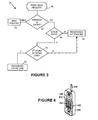
- FIG. 3 illustrates an exemplary cache management policy 48 that may be implemented by the controller 26.
- a read request may be issued to controller 26.
- Controller 26 then may determine whether the data is present in cache memory 14, as indicated by block 52.
- the controller 26 may determine that the data to be read is not present in the cache memory 14 and a "cache miss" may be generated.
- miss policies may be implemented per block 54. For example, miss policies discussed in copending application entitled “Methods and Apparatuses for Managing Memory,” filed , serial no. (Atty. Docket No.: TI-35430), may be implemented in block 54.
- the controller 26 may determine that the requested address is present in the cache memory 14 and a "cache hit" may be generated.
- Controller 26 may then determine whether the initial read request (block 50) refers to data that is part of the stack 32, sometimes called "stack data", as indicated by block 56.
- Decode logic 20, illustrated in Figure 2 may provide the controller 26 with information indicating whether the initial request for data was for stack data. In the event that the initial read request does not refer to stack data, then traditional read hit policies may be implemented as indicated by block 58. If the initial read request does refer to stack data, a determination is made as to whether the read hit corresponds to the first word in the cache line, per block 60.
- the cache line may be invalidated per block 62. Invalidating the cache line allows replacement algorithms to replace this newly invalidated cache line the next time space is needed in the cache memory 14. For instance, in a 2 way set associative cache with a LRU replacement policy, a missing line can only be loaded in two different locations within the cache. The victim location is selected by preferably one LRU bit per cache line, which specified which of the two possible lines must be replaced. If both lines are valid, the LRU indicates which line must be replaced by selecting the Least Recently Used.
- the LRU hardware selects to the invalid line by default. Therefore, by invalidating a line, the LRU bit of the corresponding line is simultaneously changed it to point to this invalidated line, when its last word is read, instead of pointing to the other line that might hold more useful data. Invalid data may be removed selectively from the cache when good data may be preserved, reducing potential unnecessary cache eviction and reload. In addition, invalidated lines are restricted from being written back to main memory 16 and therefore traffic between the cache memory 14 and the main memory 16 may be reduced by invalidating cache lines.
- the embodiments refer to situations where the stack 32 is increasing, i.e., the stack pointer incrementing as data are pushed onto the stack, the above discussion equally applies to situations where the stack 32 is decreasing, i.e., stack pointer decrementing as data are pushed onto the stack.
- checking of the last words of the cache line may be done. For example, if the stack pointer is referring to word W 0 of a cache line CL 0 , and a cache hit occurs from a read operation (e.g., as the result of popping multiple values from the stack 32), then subsequent words, i.e., W 1 , W 2 , ..., W N may also generate cache hits.
- some embodiments refer to situations where the cache replacement policy is modified while invalidating cache lines
- other embodiments include modifying the cache replacement policy without invalidating a cache line.
- the LRU policy may point to the cache line without invalidating the cache line. In this manner, the cache line may be written back to main memory 14 and valid data in the cache line may be retained. This may be accomplished by implementing the replacement policy in hardware.
- stack based operations such as pushing and popping data, may result in cache access.
- the micro-stack 25 may initiate the data stack transfer between system 10 and the cache memory 14.
- the micro-stack 25 may push and pop data from the stack 32.
- Stack operations also may be originated by a stack-management OS, which also may benefit from the disclosed cache management policies by indicating prior to the data access that data belong to a stack and thus optimizing those accesses.
- some programming languages, such as Java implement stack based operations and may benefit from the disclosed embodiments.
- system 10 may be implemented as a mobile cell phone such as that illustrated in Figure 4.
- a mobile communication device includes an integrated keypad 412 and display 414.
- the processor 12 and other components may be included in electronics package 410 connected to the keypad 412, display 414, and radio frequency (“RF") circuitry 416.
- the RF circuitry 416 may be connected to an antenna 418.
Landscapes
- Engineering & Computer Science (AREA)
- Theoretical Computer Science (AREA)
- Physics & Mathematics (AREA)
- General Engineering & Computer Science (AREA)
- General Physics & Mathematics (AREA)
- Memory System Of A Hierarchy Structure (AREA)
Abstract
Description
Claims (11)
- A method of managing memory, comprising:issuing a data request to remove data;determining whether the data is being removed from a cache line in a cache memory;determining whether the data being removed is stack data; andvarying the memory management policies depending on whether the data being removed corresponds to a predetermined word in the cache line.
- The method of claim 1, wherein the predetermined word is the first word in the cache line.
- The method of claim 2, wherein the cache line holding the stack data is queued for replacement by a replacement policy when a read hit occurs on the first word of the cache line.
- The method of claim 3, wherein the replacement policy is a least recently used (LRU) policy.
- The method of any preceding claim, wherein the cache line is a dirty cache line.
- A system, comprising:wherein the memory further comprises a cache memory and a main memory; anda memory;a controller coupled to the memory;a stack that exists in the memory;
wherein the controller adjusts its management policies depending on whether data that is being removed corresponds to a predetermined word in a cache line. - The system of claim 6, wherein the cache line is invalidated.
- The system of claim 7, wherein the invalidated cache line is queued for replacement by a replacement policy.
- The system of any claim 6-8, wherein the predetermined word is the last word in the cache line.
- The system of claim 6, the cache line is a dirty cache line.
- The system of claim 10, wherein the dirty cache line is invalidated if the predetermined word in the dirty cache line is the first word.
Priority Applications (2)
| Application Number | Priority Date | Filing Date | Title |
|---|---|---|---|
| EP03291915A EP1387278A3 (en) | 2002-07-31 | 2003-07-30 | Methods and apparatuses for managing memory |
| US10/631,205 US20040024970A1 (en) | 2002-07-31 | 2003-07-31 | Methods and apparatuses for managing memory |
Applications Claiming Priority (3)
| Application Number | Priority Date | Filing Date | Title |
|---|---|---|---|
| US40039102P | 2002-07-31 | 2002-07-31 | |
| US400391P | 2002-07-31 | ||
| EP03291915A EP1387278A3 (en) | 2002-07-31 | 2003-07-30 | Methods and apparatuses for managing memory |
Publications (2)
| Publication Number | Publication Date |
|---|---|
| EP1387278A2 true EP1387278A2 (en) | 2004-02-04 |
| EP1387278A3 EP1387278A3 (en) | 2005-03-23 |
Family
ID=38605883
Family Applications (1)
| Application Number | Title | Priority Date | Filing Date |
|---|---|---|---|
| EP03291915A Withdrawn EP1387278A3 (en) | 2002-07-31 | 2003-07-30 | Methods and apparatuses for managing memory |
Country Status (2)
| Country | Link |
|---|---|
| US (1) | US20040024970A1 (en) |
| EP (1) | EP1387278A3 (en) |
Cited By (1)
| Publication number | Priority date | Publication date | Assignee | Title |
|---|---|---|---|---|
| WO2007041145A1 (en) * | 2005-09-30 | 2007-04-12 | Intel Corporation | Instruction-assisted cache management for efficient use of cache and memory |
Families Citing this family (4)
| Publication number | Priority date | Publication date | Assignee | Title |
|---|---|---|---|---|
| US8176250B2 (en) * | 2003-08-29 | 2012-05-08 | Hewlett-Packard Development Company, L.P. | System and method for testing a memory |
| US7346755B2 (en) * | 2003-09-16 | 2008-03-18 | Hewlett-Packard Development, L.P. | Memory quality assurance |
| US9740623B2 (en) * | 2013-03-15 | 2017-08-22 | Intel Corporation | Object liveness tracking for use in processing device cache |
| US12681863B2 (en) | 2023-03-24 | 2026-07-14 | Samsung Electronics Co., Ltd. | Cache processing request for data stored in stack area by using useless information, operating method of cache, and electronic device comprising cache |
Family Cites Families (12)
| Publication number | Priority date | Publication date | Assignee | Title |
|---|---|---|---|---|
| US5307477A (en) * | 1989-12-01 | 1994-04-26 | Mips Computer Systems, Inc. | Two-level cache memory system |
| US5479636A (en) * | 1992-11-16 | 1995-12-26 | Intel Corporation | Concurrent cache line replacement method and apparatus in microprocessor system with write-back cache memory |
| US6151661A (en) * | 1994-03-03 | 2000-11-21 | International Business Machines Corporation | Cache memory storage space management system and method |
| DK0938703T3 (en) * | 1996-11-13 | 2003-08-18 | Paran Arik | Accelerator for real-time programming language |
| US6098089A (en) * | 1997-04-23 | 2000-08-01 | Sun Microsystems, Inc. | Generation isolation system and method for garbage collection |
| GB9907283D0 (en) * | 1999-03-31 | 1999-05-26 | Koninkl Philips Electronics Nv | Memory reclamation method |
| EP1182565B1 (en) * | 2000-08-21 | 2012-09-05 | Texas Instruments France | Cache and DMA with a global valid bit |
| EP1182562B1 (en) * | 2000-08-21 | 2011-05-11 | Texas Instruments France | Smartcache with interruptible block prefetch |
| US6567905B2 (en) * | 2001-01-23 | 2003-05-20 | Gemstone Systems, Inc. | Generational garbage collector with persistent object cache |
| US6748495B2 (en) * | 2001-05-15 | 2004-06-08 | Broadcom Corporation | Random generator |
| EP1304620A1 (en) * | 2001-10-17 | 2003-04-23 | Texas Instruments Incorporated | Cache with selective write allocation |
| US7065613B1 (en) * | 2002-06-06 | 2006-06-20 | Maxtor Corporation | Method for reducing access to main memory using a stack cache |
-
2003
- 2003-07-30 EP EP03291915A patent/EP1387278A3/en not_active Withdrawn
- 2003-07-31 US US10/631,205 patent/US20040024970A1/en not_active Abandoned
Cited By (2)
| Publication number | Priority date | Publication date | Assignee | Title |
|---|---|---|---|---|
| WO2007041145A1 (en) * | 2005-09-30 | 2007-04-12 | Intel Corporation | Instruction-assisted cache management for efficient use of cache and memory |
| US7437510B2 (en) | 2005-09-30 | 2008-10-14 | Intel Corporation | Instruction-assisted cache management for efficient use of cache and memory |
Also Published As
| Publication number | Publication date |
|---|---|
| US20040024970A1 (en) | 2004-02-05 |
| EP1387278A3 (en) | 2005-03-23 |
Similar Documents
| Publication | Publication Date | Title |
|---|---|---|
| US11074190B2 (en) | Slot/sub-slot prefetch architecture for multiple memory requestors | |
| US7546437B2 (en) | Memory usable in cache mode or scratch pad mode to reduce the frequency of memory accesses | |
| EP1643506B1 (en) | System and method for automatically saving memory contents of a data processing device on power failure | |
| US7552286B2 (en) | Performance of a cache by detecting cache lines that have been reused | |
| JP4486750B2 (en) | Shared cache structure for temporary and non-temporary instructions | |
| US5958040A (en) | Adaptive stream buffers | |
| US20210056030A1 (en) | Multi-level system memory with near memory capable of storing compressed cache lines | |
| US6272597B1 (en) | Dual-ported, pipelined, two level cache system | |
| CN101595462B (en) | Apparatus and method to reduce throws in a multi-level cache hierarchy | |
| US7809889B2 (en) | High performance multilevel cache hierarchy | |
| EP2478441B1 (en) | Read and write aware cache | |
| US20060004984A1 (en) | Virtual memory management system | |
| US5737751A (en) | Cache memory management system having reduced reloads to a second level cache for enhanced memory performance in a data processing system | |
| EP1581876B1 (en) | Memory controller and method for writing to a memory | |
| US7117306B2 (en) | Mitigating access penalty of a semiconductor nonvolatile memory | |
| US5809526A (en) | Data processing system and method for selective invalidation of outdated lines in a second level memory in response to a memory request initiated by a store operation | |
| US20040221117A1 (en) | Logic and method for reading data from cache | |
| EP1387277B1 (en) | Write back policy for memory | |
| US20040024970A1 (en) | Methods and apparatuses for managing memory | |
| US20040024969A1 (en) | Methods and apparatuses for managing memory | |
| US7203797B2 (en) | Memory management of local variables | |
| US7330937B2 (en) | Management of stack-based memory usage in a processor | |
| EP1387276A2 (en) | Methods and apparatus for managing memory | |
| US8117393B2 (en) | Selectively performing lookups for cache lines | |
| HK1088990A1 (en) | System and method for automatically saving memory contents of a data processing device on power failure |
Legal Events
| Date | Code | Title | Description |
|---|---|---|---|
| PUAI | Public reference made under article 153(3) epc to a published international application that has entered the european phase |
Free format text: ORIGINAL CODE: 0009012 |
|
| AK | Designated contracting states |
Kind code of ref document: A2 Designated state(s): AT BE BG CH CY CZ DE DK EE ES FI FR GB GR HU IE IT LI LU MC NL PT RO SE SI SK TR |
|
| AX | Request for extension of the european patent |
Extension state: AL LT LV MK |
|
| PUAL | Search report despatched |
Free format text: ORIGINAL CODE: 0009013 |
|
| AK | Designated contracting states |
Kind code of ref document: A3 Designated state(s): AT BE BG CH CY CZ DE DK EE ES FI FR GB GR HU IE IT LI LU MC NL PT RO SE SI SK TR |
|
| AX | Request for extension of the european patent |
Extension state: AL LT LV MK |
|
| RIC1 | Information provided on ipc code assigned before grant |
Ipc: 7G 06F 12/08 B Ipc: 7G 06F 12/12 A |
|
| RAP1 | Party data changed (applicant data changed or rights of an application transferred) |
Owner name: TEXAS INSTRUMENTS FRANCE Owner name: TEXAS INSTRUMENTS INC. |
|
| 17P | Request for examination filed |
Effective date: 20050923 |
|
| AKX | Designation fees paid |
Designated state(s): DE FR GB |
|
| STAA | Information on the status of an ep patent application or granted ep patent |
Free format text: STATUS: THE APPLICATION HAS BEEN WITHDRAWN |
|
| 18W | Application withdrawn |
Effective date: 20090612 |