EP1385288A2 - Interleaver-based multiplexer and demultiplexer - Google Patents
Interleaver-based multiplexer and demultiplexer Download PDFInfo
- Publication number
- EP1385288A2 EP1385288A2 EP03004843A EP03004843A EP1385288A2 EP 1385288 A2 EP1385288 A2 EP 1385288A2 EP 03004843 A EP03004843 A EP 03004843A EP 03004843 A EP03004843 A EP 03004843A EP 1385288 A2 EP1385288 A2 EP 1385288A2
- Authority
- EP
- European Patent Office
- Prior art keywords
- signals
- channel
- interleaved
- multiplexed
- channels
- Prior art date
- Legal status (The legal status is an assumption and is not a legal conclusion. Google has not performed a legal analysis and makes no representation as to the accuracy of the status listed.)
- Withdrawn
Links
Images



Classifications
-
- H—ELECTRICITY
- H04—ELECTRIC COMMUNICATION TECHNIQUE
- H04J—MULTIPLEX COMMUNICATION
- H04J14/00—Optical multiplex systems
- H04J14/02—Wavelength-division multiplex systems
- H04J14/03—WDM arrangements
- H04J14/0307—Multiplexers; Demultiplexers
Definitions
- the present invention relates to optical communication devices. More specifically, the present invention relates to optical multiplexer and demultiplexer.
- a wavelength demultiplexer 10, illustrated in Figure 1 is a device with one input port and N output ports, N being a number greater than one.
- the input port receives, from an input fiber (transmission medium) an N-channel wavelength-division multiplexed (WDM) signal 11. That is, the input WDM signal 11 includes N different channels, each channel modulated onto an optical carrier with a different wavelength.
- WDM wavelength-division multiplexed
- each channel is represented as L i where i ranges from 1 to N.
- N can be eight, in which case the demultiplexer 10 is referred to as an 8-channel demultiplexer.
- the channels of a WDM signal are spaced in frequency, and the channel spacing is designated, for convenience, as D.
- the demultiplexer 10 directs each of the N channels (wavelengths) to a different output port, thus separating, or demultiplexing, the input channels.
- a wavelength multiplexer (not illustrated) performs the reverse operation. That is, a multiplexer combines N channels onto a single WDM signal.
- this document discusses demultiplexers; however, it is understood that the following discussions also apply to multiplexers.
- the demultiplexer 10 is described as an N-channel device because it can demultiplex (separate) a WDM signal having N channels with wavelength spacing D between the channels.
- Properties (for example, cost, size, and optical loss) of demultiplexers often scale strongly with number of channels and spacing requirement. That is, a multiplexer having larger number of channels or requiring demultiplexing of closely spaced channels require more real estate (larger size), has higher cost, and introduces more signal loss than a multiplexer having relatively smaller number of channels, greater spacing between channels, or both.
- An interleaver 20 of Figure 2 is a three-port wavelength-separation device that divides a single input WDM signal 21 into two de-interleaved WDM signals 23 and 25, first de-interleaved output signal 23 having the odd channels of the input WDM signal 21 and the second de-interleaved output signal 25 having the even channels of the input WDM signal 21.
- the first de-interleaved output signal 23 is a WDM signal including the odd channels L 1 , L 3 , L 5 , and L 7
- the second de-interleaved output signal 25 is a WDM signal including the even channels L 2 , L 4 , L 6 , and L 8 .
- an interleaver is described in B. N. Dingel and T. Aruga, "Properties of a novel, noncascaded-type easy-to-design, ripple-free optical bandpass filter," IEEE Journal of Lightwave Technology, Vol. 7, No. 8, August 1999, pp. 1461-1469.
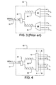
- One technique to build a wavelength demultiplexing system for large N, small D, or a combination of large N and small D is to use one or more stages of interleavers followed by demultiplexers as shown in Figure 3.
- a demultiplexer system 30 is illustrated.
- An interleaver 30 divides an input WDM signal 31 having 8 channels with a first channel spacing D 1 into two 4-channel WDM signals 33 and 35 each having four channels with spacing D 2 where D 2 is twice that of D 1 .
- each of the 4-channel WDM signals 33 and 35 are demultiplexed by one of the 4-channel demultiplexers 34 and 36, respectively.
- the number of channels of the input signals (the 4-channel WDM signals 33 and 35) for each of the 4-channel demultiplexers 34 and 36 are relatively small compared to the number of channels of the WDM input signal 31 (or input signal 11 for the 8-channel demultiplexer 10 of Figure 1).
- the spacing D 2 between the channels of the input signals (the 4-channel WDM signals 33 and 35) is wider than the spacing D 1 of the input WDM 8-channel signal 31 (or input signal 11 of Figure 1).
- the demultiplexer system 30 can be fabricated having more desirable properties than the properties of the demultiplexer 10 of Figure 1.
- a demultiplexer system includes an interleaver for dividing an input multiplexed signal (having a plurality of channels) into two de-interleaved multiplexed signals (each de-interleaved multiplexed signal having a subset of the channels of the input signal).
- a single demultiplexing device separates both of the de-interleaved multiplexed signals into single-channel output signals.
- a method for demultiplexing an N-channel multiplexed signal is disclosed. First, the N-channel multiplexed signal is divided into two M-channel multiplexed signals where M is one half of M. Then, both of the M-channel signals are separated into single-channel output signals using a single demultiplexing device.
- a demultiplexer system includes a first-stage interleaver dividing an input multiplexed signal (having a plurality of channels) into two de-interleaved multiplexed signals. Then, each of two second-stage interleavers divides one of the de-interleaved multiplexed signals into two twice-de-interleaved multiplexed signals. Finally, a single demultiplexing device demultiplexes the twice-de-interleaved multiplexed signals into single-channel output signals.
- a demultiplexer system includes a first-stage interleaver dividing an input multiplexed signal (having a plurality of channels) into two de-interleaved multiplexed signals. Then, each of two second-stage interleavers divides one of the de-interleaved multiplexed signals into two twice-de-interleaved multiplexed signals. Finally, a single demultiplexing device demultiplexes the twice-de-interleaved multiplexed signals into single-channel output signals.
- a multiplexer system includes a single multiplexing device for multiplexing a first set of single-channel signals into a first multiplexed signal and a second set of singled-channel signals into a second multiplexed signal.
- An interleaver combines the first multiplexed signal and the second multiplexed signal into a third multiplexed signal.
- the present invention is embodied in apparatus and techniques for fabricating demultiplexer ad multiplexer systems while minimizing the number and coost of the required components.
- Figure 4 is a diagram of an 8-channel demultiplexer system 40 according to one embodiment of the present invention. Portions of the system 40 are similar to portions of the demultiplexer system 30 of Figure 3. For convenience, components in Figure 4 that are similar to components in Figure 3 are assigned the same reference numerals and different components are assigned different reference numerals.
- the system 40 includes an interleaver 32 for dividing an input multiplexed signal 31 having a plurality of channels into two de-interleaved multiplexed signals 33 and 35, each de-interleaved multiplexed signal 33 and 35 having a subset of said plurality of channels.
- the input signal is an 8-channel WDM signal having channels L1 through L8. It is divided into the first de-interleaved multiplexed signal 33 having the odd channels (four channels) including channels L 1 , L 3 , L 5 , and L 7 and the second de-interleaved multiplexed signal 35 having the even channels (four channels) including channels L 2 , L 4 , L 6 , and L 8 .
- the number of channels of the de-interleaved signal referable as M, is half of the number of channels of the input signal 31.
- Both of the de-interleaved multiplexed signals 33 and 35 are demultiplexed using a single demultiplexing device 42.
- the device 42 separates both de-interleaved multiplexed signals 33 and 35 into single-channel output signals.
- the single demultiplexing device 42 replaces two demultiplexers 34 and 36 of system 30 of Figure 3.
- Figure 5 is a side view of a single demultiplexing device 42 of Figure 4 as viewed from line A--A of Figure 4. As illustrated, the device 42 is implemented using such devices as an Offner spectrograph.
- the device 42 can be considered as a stacked demultiplexer where its inputs are a one-dimensional array (a vertical column) of multiplexed signals such as signals 33 and 35 and its output is a two-dimensional array of demultiplexed, single-channel signals.
- FIG. 6 is a diagram of a 16-channel demultiplexer system 50 according to another embodiment of the present invention.
- input 16-channel WDM signal 51 having wavelength spacing D 3 is demultiplexed by the system 50.
- the input signal 51 is divided into two de-interleaved multiplexed signals 61 and 71 by a first-stage interleaver 52.
- Each of the de-interleaved multiplexed signals 61 and 71 are 8-channel WDM signals having channel spacing of D 4 where D 4 is twice the value of D 3 .
- a first second-stage interleaver 60 divides the first de-interleaved multiplexed signal 61 into two twice-de-interleaved multiplexed signals 63 and 65.
- Each of the twice-de-interleaved multiplexed signals 63 and 65 are 4-channel WDM signals having channel spacing of D 5 that is twice the value of D 4 .
- a second second-stage interleaver 70 divides the second de-interleaved multiplexed signal 71 into two twice-de-interleaved multiplexed signals 73 and 75.
- Each of the twice-de-interleaved multiplexed signals 73 and 75 are 4-channel WDM signals having channel spacing of D 5 that is twice the value of D 4 .
- a single demultiplexing device 80 demultiplexes all four twice-de-interleaved multiplexed signals 63, 65, 73, and 75 into single-channel output signals.
- the device 80 is, for example, an Offner spectrograph.
- a multiplexer system 90 is illustrated.
- a single multiplexing device 92 multiplexes a first set of single-channel signals L 1 , L 3 , L 5 , and L 7 into a first multiplexed signal 93.
- the same multiplexing device 92 multiplexes a second set of single-channel signals L 2 , L 4 , L 6 , and L 8 into a second multiplexed signal 95.
- the multiplexed signals 93 and 95 are combined by an interleaver 94 into a third multiplexed signal 97 having all eight channels L 1 , L 2 , ... L 8 .
Landscapes
- Engineering & Computer Science (AREA)
- Computer Networks & Wireless Communication (AREA)
- Signal Processing (AREA)
- Optical Communication System (AREA)
Abstract
Description
Claims (8)
- A demultiplexer system (40) comprising:an interleaver (32) for dividing an input multiplexed signal (31) having a plurality of channels into two de-interleaved multiplexed signals (33, 35), each de-interleaved multiplexed signal having a subset of said plurality of channels; anda single demultiplexing device (42) for separating both said de-interleaved multiplexed signals (33, 35) into single-channel output signals.
- The demultiplexer system (40) recited in claim 1 wherein the single demultiplexing device (42) is an Offner spectrograph.
- A method for demultiplexing an N-channel multiplexed signal, the method comprising:dividing the N-channel multiplexed signal (31) into two M-channel multiplexed signals (33, 35) where M is one half of M; andseparating both of said M-channel signals (33, 35) into single-channel output signals using a single demultiplexing device (42).
- The demultiplexer method recited in claim 3 wherein the single demultiplexing device (42) is an Offner spectrograph.
- A demultiplexer system (50) comprising:a first-stage interleaver (52) dividing an input multiplexed signal (51) having a plurality of channels into two de-interleaved multiplexed signals (61, 71),two second-stage interleavers (60, 70), each second-stage interleaver dividing one of said de-interleaved multiplexed signals into two twice-de-interleaved multiplexed signals;a single demultiplexing device (80) for demultiplexing said twice-de-interleaved multiplexed signals into single-channel output signals.
- The demultiplexer system (50) recited in claim 5 wherein the single demultiplexing device (80) is an Offner spectrograph.
- A multiplexer system comprising:a single multiplexing device for multiplexing a first set of single-channel signals into a first multiplexed signal and a second set of singled-channel signals into a second multiplexed signal; andan interleaver for combining said first multiplexed signal and said second multiplexed signal into a third multiplexed signal.
- The multiplexer system recited in claim 7 wherein the single multiplexing device is an Offner spectrograph.
Applications Claiming Priority (2)
| Application Number | Priority Date | Filing Date | Title |
|---|---|---|---|
| US206450 | 2002-07-26 | ||
| US10/206,450 US20040018019A1 (en) | 2002-07-26 | 2002-07-26 | Interleaver-based multiplexer and demultiplexer |
Publications (2)
| Publication Number | Publication Date |
|---|---|
| EP1385288A2 true EP1385288A2 (en) | 2004-01-28 |
| EP1385288A3 EP1385288A3 (en) | 2006-10-18 |
Family
ID=30000125
Family Applications (1)
| Application Number | Title | Priority Date | Filing Date |
|---|---|---|---|
| EP03004843A Withdrawn EP1385288A3 (en) | 2002-07-26 | 2003-03-05 | Interleaver-based multiplexer and demultiplexer |
Country Status (3)
| Country | Link |
|---|---|
| US (1) | US20040018019A1 (en) |
| EP (1) | EP1385288A3 (en) |
| JP (1) | JP2004064781A (en) |
Families Citing this family (4)
| Publication number | Priority date | Publication date | Assignee | Title |
|---|---|---|---|---|
| US7088885B1 (en) * | 2002-11-13 | 2006-08-08 | Finisar Corporation | System for modulating optical signals |
| KR100539893B1 (en) * | 2003-11-12 | 2005-12-28 | 삼성전자주식회사 | Optical transmitter for dense wavelength division multiplexing |
| US8285144B2 (en) * | 2009-07-30 | 2012-10-09 | Jds Uniphase Corporation | Optical device for rearranging wavelength channels |
| US11621784B1 (en) * | 2021-09-29 | 2023-04-04 | X Development Llc | Photonic integrated circuit with optical deinterleaver |
Family Cites Families (6)
| Publication number | Priority date | Publication date | Assignee | Title |
|---|---|---|---|---|
| AU4406299A (en) * | 1998-04-29 | 1999-11-16 | American Holographic, Inc. | Corrected concentric spectrometer |
| US6130971A (en) * | 1998-08-06 | 2000-10-10 | Avanex Corporation | Fiber optic dense wavelength division multiplexer with a phase differential method of wavelength separation utilizing a polarization beam splitter and a nonlinear interferometer |
| US6263127B1 (en) * | 1999-05-13 | 2001-07-17 | Lucent Technologies Inc. | Free-space/arrayed-waveguide router |
| US6678476B1 (en) * | 2000-10-30 | 2004-01-13 | Oplink Communications, Inc. | WDM with optical interleaving for increased channel capacity |
| US6658212B1 (en) * | 2000-10-31 | 2003-12-02 | Agilent Technologies, Inc. | Polarization-independent, configurable optical multiplexer |
| FR2818059B1 (en) * | 2000-12-07 | 2003-02-07 | Cit Alcatel | DEVICE FOR DEMULTIPLEXING FREQUENCY BANDS |
-
2002
- 2002-07-26 US US10/206,450 patent/US20040018019A1/en not_active Abandoned
-
2003
- 2003-03-05 EP EP03004843A patent/EP1385288A3/en not_active Withdrawn
- 2003-07-11 JP JP2003273494A patent/JP2004064781A/en not_active Withdrawn
Also Published As
| Publication number | Publication date |
|---|---|
| US20040018019A1 (en) | 2004-01-29 |
| EP1385288A3 (en) | 2006-10-18 |
| JP2004064781A (en) | 2004-02-26 |
Similar Documents
| Publication | Publication Date | Title |
|---|---|---|
| US5608825A (en) | Multi-wavelength filtering device using optical fiber Bragg grating | |
| US6067178A (en) | Multiple wavelength division multiplexer with reduced loss | |
| JP4588234B2 (en) | Optical device and wavelength division multiplexing communication system using the same | |
| US20160164625A1 (en) | Distributed wave division multiplexing systems | |
| US20030002102A1 (en) | Device for frequency band demultiplexing | |
| US20030123880A1 (en) | Programmable OADM with chromatic dispersion, dispersion slope and amplitude ripple compensation, and method | |
| US20020150329A1 (en) | Multi-channel wavelength division multiplexer/demultiplexer | |
| KR100400362B1 (en) | Apparatus for optical add drop multiplexing and WDM optical network comprising it | |
| US6243179B1 (en) | Banded add drop device | |
| EP1261160A2 (en) | Optical add drop multiplexer | |
| US20030206743A1 (en) | Cross connecting device and optical communication system | |
| US20050013615A1 (en) | Optical add-drop apparatus and method | |
| US6546166B1 (en) | Multi-stage optical DWDM channel group interleaver | |
| US20040018019A1 (en) | Interleaver-based multiplexer and demultiplexer | |
| EP1076471B1 (en) | Optical wavelength division multiplexing transmission network device | |
| EP1009120A2 (en) | Multichannel optical ADD/DROP, multiplexor/demultiplexor | |
| JP5312553B2 (en) | Optical add / drop multiplexer | |
| US6519384B2 (en) | Optical communication network | |
| US20020110314A1 (en) | System and method for narrow channel spaced dense wavelength division multiplexing/demultiplexing | |
| KR100323058B1 (en) | Optical add and drop multiplexer | |
| US6782156B2 (en) | Interleaved band demultiplexing/multiplexing system | |
| JP2003185876A (en) | Wavelength multiplexer and wavelength multiplexer | |
| JP2000147281A (en) | Optical multiplexer / demultiplexer | |
| JP2000224108A (en) | Wavelength division multiple demultiplexer | |
| US6400861B1 (en) | Optical demultiplexer architecture |
Legal Events
| Date | Code | Title | Description |
|---|---|---|---|
| PUAI | Public reference made under article 153(3) epc to a published international application that has entered the european phase |
Free format text: ORIGINAL CODE: 0009012 |
|
| AK | Designated contracting states |
Kind code of ref document: A2 Designated state(s): AT BE BG CH CY CZ DE DK EE ES FI FR GB GR HU IE IT LI LU MC NL PT RO SE SI SK TR |
|
| AX | Request for extension of the european patent |
Extension state: AL LT LV MK |
|
| PUAL | Search report despatched |
Free format text: ORIGINAL CODE: 0009013 |
|
| AK | Designated contracting states |
Kind code of ref document: A3 Designated state(s): AT BE BG CH CY CZ DE DK EE ES FI FR GB GR HU IE IT LI LU MC NL PT RO SE SI SK TR |
|
| AX | Request for extension of the european patent |
Extension state: AL LT LV MK |
|
| RAP1 | Party data changed (applicant data changed or rights of an application transferred) |
Owner name: AVAGO TECHNOLOGIES FIBER IP (SINGAPORE) PTE. LTD. |
|
| AKX | Designation fees paid | ||
| STAA | Information on the status of an ep patent application or granted ep patent |
Free format text: STATUS: THE APPLICATION IS DEEMED TO BE WITHDRAWN |
|
| 18D | Application deemed to be withdrawn |
Effective date: 20070419 |
|
| REG | Reference to a national code |
Ref country code: DE Ref legal event code: 8566 |