EP1385031A2 - Wavelength filter, variable wavelength filter, and optical device - Google Patents
Wavelength filter, variable wavelength filter, and optical device Download PDFInfo
- Publication number
- EP1385031A2 EP1385031A2 EP03254464A EP03254464A EP1385031A2 EP 1385031 A2 EP1385031 A2 EP 1385031A2 EP 03254464 A EP03254464 A EP 03254464A EP 03254464 A EP03254464 A EP 03254464A EP 1385031 A2 EP1385031 A2 EP 1385031A2
- Authority
- EP
- European Patent Office
- Prior art keywords
- wavelength filter
- lattice structures
- variable wavelength
- wavelength
- filters
- Prior art date
- Legal status (The legal status is an assumption and is not a legal conclusion. Google has not performed a legal analysis and makes no representation as to the accuracy of the status listed.)
- Withdrawn
Links
Images



Classifications
-
- G—PHYSICS
- G02—OPTICS
- G02B—OPTICAL ELEMENTS, SYSTEMS OR APPARATUS
- G02B5/00—Optical elements other than lenses
- G02B5/20—Filters
- G02B5/26—Reflecting filters
-
- G—PHYSICS
- G02—OPTICS
- G02B—OPTICAL ELEMENTS, SYSTEMS OR APPARATUS
- G02B6/00—Light guides; Structural details of arrangements comprising light guides and other optical elements, e.g. couplings
- G02B6/10—Light guides; Structural details of arrangements comprising light guides and other optical elements, e.g. couplings of the optical waveguide type
- G02B6/12—Light guides; Structural details of arrangements comprising light guides and other optical elements, e.g. couplings of the optical waveguide type of the integrated circuit kind
- G02B6/12007—Light guides; Structural details of arrangements comprising light guides and other optical elements, e.g. couplings of the optical waveguide type of the integrated circuit kind forming wavelength selective elements, e.g. multiplexer, demultiplexer
-
- G—PHYSICS
- G02—OPTICS
- G02B—OPTICAL ELEMENTS, SYSTEMS OR APPARATUS
- G02B6/00—Light guides; Structural details of arrangements comprising light guides and other optical elements, e.g. couplings
- G02B6/24—Coupling light guides
- G02B6/26—Optical coupling means
- G02B6/28—Optical coupling means having data bus means, i.e. plural waveguides interconnected and providing an inherently bidirectional system by mixing and splitting signals
- G02B6/293—Optical coupling means having data bus means, i.e. plural waveguides interconnected and providing an inherently bidirectional system by mixing and splitting signals with wavelength selective means
- G02B6/29346—Optical coupling means having data bus means, i.e. plural waveguides interconnected and providing an inherently bidirectional system by mixing and splitting signals with wavelength selective means operating by wave or beam interference
- G02B6/29361—Interference filters, e.g. multilayer coatings, thin film filters, dichroic splitters or mirrors based on multilayers, WDM filters
- G02B6/29362—Serial cascade of filters or filtering operations, e.g. for a large number of channels
- G02B6/29364—Cascading by a light guide path between filters or filtering operations, e.g. fibre interconnected single filter modules
-
- G—PHYSICS
- G02—OPTICS
- G02B—OPTICAL ELEMENTS, SYSTEMS OR APPARATUS
- G02B6/00—Light guides; Structural details of arrangements comprising light guides and other optical elements, e.g. couplings
- G02B6/24—Coupling light guides
- G02B6/26—Optical coupling means
- G02B6/28—Optical coupling means having data bus means, i.e. plural waveguides interconnected and providing an inherently bidirectional system by mixing and splitting signals
- G02B6/293—Optical coupling means having data bus means, i.e. plural waveguides interconnected and providing an inherently bidirectional system by mixing and splitting signals with wavelength selective means
- G02B6/29346—Optical coupling means having data bus means, i.e. plural waveguides interconnected and providing an inherently bidirectional system by mixing and splitting signals with wavelength selective means operating by wave or beam interference
- G02B6/29361—Interference filters, e.g. multilayer coatings, thin film filters, dichroic splitters or mirrors based on multilayers, WDM filters
- G02B6/29368—Light guide comprising the filter, e.g. filter deposited on a fibre end
-
- G—PHYSICS
- G02—OPTICS
- G02B—OPTICAL ELEMENTS, SYSTEMS OR APPARATUS
- G02B6/00—Light guides; Structural details of arrangements comprising light guides and other optical elements, e.g. couplings
- G02B6/24—Coupling light guides
- G02B6/26—Optical coupling means
- G02B6/28—Optical coupling means having data bus means, i.e. plural waveguides interconnected and providing an inherently bidirectional system by mixing and splitting signals
- G02B6/293—Optical coupling means having data bus means, i.e. plural waveguides interconnected and providing an inherently bidirectional system by mixing and splitting signals with wavelength selective means
- G02B6/29379—Optical coupling means having data bus means, i.e. plural waveguides interconnected and providing an inherently bidirectional system by mixing and splitting signals with wavelength selective means characterised by the function or use of the complete device
- G02B6/29395—Optical coupling means having data bus means, i.e. plural waveguides interconnected and providing an inherently bidirectional system by mixing and splitting signals with wavelength selective means characterised by the function or use of the complete device configurable, e.g. tunable or reconfigurable
Definitions
- the present invention generally relates to a wavelength filter, a variable wavelength filter, and an optical device that includes the wavelength filter or the variable wavelength filter, and more particularly, to a reflection wavelength filter, a variable wavelength filter, and an optical device that includes the wavelength filter or the variable wavelength filter.
- Figs. 1A through 1D illustrate a conventional wavelength filter that will be hereinafter referred to as prior art 1.
- the wavelength filter of prior art 1 is an optical device that includes dielectric multilayer filters. To achieve a higher wavelength selectivity, it is necessary to employ a large number of layers in the wavelength filter. To do so, however, high production costs are required.
- the wavelength filter of prior art 1 has a fixed reflection wavelength range.
- the rotation with respect to the optical axis of the wavelength filter needs to be varied using a mechanical structure. Therefore, the optical axis of the light incident on the wavelength filter needs to be varied using a mechanical structure.
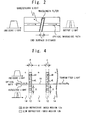
- the wavelength filter of prior art 1 is a transmission-type optical device. To apply this wavelength filter to optical communications, it is necessary to physically cut the optical waveguide path, which is the transmitting part, as shown in Fig. 2. In a case where the optical waveguide path is cut to accommodate a wavelength filter, as shown in Fig. 2, the light transmission loss becomes greater. To reduce the light transmission loss, the wavelength filter should be formed by a reflection optical device that reflects a specific wavelength in narrow bands. However, this method has not been established in the prior art.
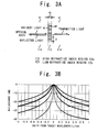
- Fig. 3A shows an example of reflection characteristics that can be typically obtained by a calculation utilizing RCWA (Rigorous Coupled-Wave Analysis) performed on the wavelength filter of prior art 2.
- RCWA Ragorous Coupled-Wave Analysis
- the reflection wavelength filter of prior art 2 has a problem that a large enough reflection to cover a desired frequency band fb cannot be secured, because the reflectivity greatly decreases with a small change in the wavelength. For this reason, it has been difficult to employ the wavelength filter of prior art 2 for communications.
- variable wavelength filter that reflects light in a frequency band wide enough for communications and has variable wavelength selectivity, and an optical device that includes the variable wavelength filter.
- a wavelength filter comprising a plurality of lattice structures that are arranged at predetermined intervals in the direction of an optical axis, each of the lattice structures having regions of two different refractive indices that are alternately arranged.
- variable wavelength filter comprising a plurality of lattice structures that are arranged at predetermined intervals in the direction of an optical axis, each of the lattice structures having regions of two different substances that are alternately arranged, and at least one of the substances being an electrooptical material.
- an optical device comprising one or more wavelength filters that are formed on a single substrate, each of the wavelength filters including a plurality of lattice structures that are arranged at predetermined intervals in the direction of an optical axis, and each of the lattice structures having regions of two different refractive indices that are alternately arranged.
- an optical device comprising one or more variable wavelength filters that are formed on a single substrate, each of the variable wavelength filters including a plurality of lattice structures that are arranged at predetermined intervals in the direction of an optical axis, each of the lattice structures having regions of two different substances that are alternately arranged, and at least one of the substances being an electrooptical material.
- Fig. 4 is a schematic view of a wavelength filter in accordance with a first embodiment of the present invention.
- the wavelength filter 1 of this embodiment includes two or more lattice filters 12 arranged at predetermined intervals in the direction of light (hereinafter referred to as the optical axis direction).
- the predetermined intervals may be uniform or varied.
- Each of the lattice filters 12 has a lattice structure in which materials of different refractive indices (high-refractive-index regions 12a and low-refractive-index regions 12b) are alternately arranged in the direction perpendicular to the optical axis 10.
- nH represents the refractive index of each high-refractive-index region 12a
- nL represents the refractive index of each low-refractive-index region 12b (nL ⁇ nH).
- the average value n ave of the refractive indexes nH and nL of the high-refractive-index regions 12a and the low-refractive-index regions 12b is higher than the refractive index n 1 of the optical waveguide path 14, and the refractive index nL is equal to or higher than the refractive index n 1 of the optical waveguide path 14. Further, the pitch among the high-refractive-index regions 12a and the low-refractive-index regions 12b (the pitch will be hereinafter referred to as the pitch length A) is shorter than the wavelength to be reflected (this wavelength will be hereinafter referred to as the target wavelength ⁇ 0 ).
- the average refractive index n ave is varied with the polarization of light to be used.
- Each of the lattice filters 12 has a predetermined thickness d in the direction of the optical axis.
- the value of the thickness d should satisfy the following equation (1) that involves the average value n ave of the refractive indices of the high-refractive-index regions 12a and the low-refractive-index regions 12b, and the target wavelength ⁇ 0 .
- n ave ⁇ d ⁇ 0 /2
- the value of the distance between each two lattice filters 12 arranged on the optical axis (this distances will be hereinafter referred to as the gap g) should satisfy the following equation (2).
- g g 0 + N ⁇ ( ⁇ 0 /n 1 )
- n 1 represents the refractive index of the material that forms the medium (the optical waveguide path 14) interposed between each two lattice filters 12
- ⁇ 0 represents the target wavelength
- g 0 represents the shortest distance among the gaps g that causes reflections in this embodiment
- N represents a positive integer. It is to be noted that the value obtained by this equation is merely used as a yardstick, and that a margin of approximately 10% is allowed in practice.
- the wavelength filter 1 of this embodiment can achieve an improved wavelength selectivity.
- the wavelength filter 1 can reflect only the neighborhood of the desired target wavelength ⁇ 0 (i.e., filtering).
- the optical waveguide path 14 is directly connected to the lattice filters 12, and may be formed by optical fibers, for example. In such a case, the same effects as the above can be obtained.
- wavelength filter 1a In the following, a more specific example of the wavelength filter 1 in accordance with this embodiment will be described.
- the specific example wavelength filter will be referred to as the wavelength filter 1a.
- Fig. 5A is a sectional view of an example structure formed along the optical axis of the wavelength filter 1a having two lattice filters 12.
- Fig. 5B is a graph showing the reflection characteristics that were obtained by a calculation utilizing RCWA performed on the example structure shown in Fig. 5A.
- the target wavelength ⁇ 0 is 1550 ⁇ m.
- the refractive index n 1 of the optical waveguide path 14 is 1.52, the refractive index nH of the high-refractive-index regions 12a is 2.0, and the refractive index nL of the low-refractive-index regions 12b is 1.96.
- the thickness d of each of the lattice filters 12 is 391.4 nm, the pitch length A among the high-refractive-index regions 12a and the low-refractive-index region 12b is 888.13 nm, and the gap g is 1780 nm.
- the wavelength filter 1a exhibits improved reflection characteristics in the neighborhood of the target wavelength ⁇ 0 .
- this specific example realizes the reflection wavelength filter 1a that can surely reflect.
- a desired frequency band fb having a predetermined width from the target wavelength ⁇ 0 .
- the desired frequency band fb is a specific wavelength band normally required in optical communications.
- Fig. 6 illustrates an example of an optical device (a wavelength filter device 100) in which the wavelength filter 1a and the optical waveguide path 14 are formed on the same substrate.
- the incident light introduced through an optical waveguide guide path 14a is reflected according to the reflection characteristics of the wavelength filter 1a having the two lattice filters 12.
- the reflected light is then outputted through an optical waveguide path 14b.
- the transmitted light that has been transmitted through the two lattice filters 12 is either absorbed by the wavelength filter device 100 or outputted.
- Figs. 7A through 7E and Figs. 8A through 8E are sectional views of the structure of Fig. 6, taken along the line A-A'.
- Figs. 7E and Figs. 8A through 8E are sectional views of the structure of Fig. 6, taken along the line B-B'.
- a layer of resist 81 is first deposited on an LN(LiTaO 3 ) substrate 80, and is then exposed through a pattern for forming the high-refractive-index regions 12a, as shown in Fig. 7A.
- Ti is vapor-deposited on the patterned surface so as to form a Ti film 82, as shown in Fig. 7B.
- the remaining resist 81 is then removed, and liftoff is performed on the Ti film 82 vapor-deposited on the resist 81, as shown in Fig. 7C.
- Annealing is then performed on the remaining parts of the Ti film 82, so as to diffuse the deposited Ti, as shown in Fig. 7D.
- the high-refractive-index regions 12a are formed, and the pattern of the high-refractive-index regions 12a and the low-refractive-index regions 12b is established.
- LN is the material for the low-refractive-index regions 12b
- LN diffused with Ti is the material for the high-refractive-index regions 12a.
- a layer of resist 84 is deposited on the surface and is then exposed through a pattern for forming the lattice filters 12, as shown in Fig. 7E. Etching is then performed, using RIE (reactive Ion Etching) or ion million, on the parts from which the resist 84 has been removed, as shown in Fig. 8A.
- RIE reactive Ion Etching
- a SiO 2 film 86 is deposited on the surface by a sputtering method or the like, as shown in Fig. 8B. Further, a SiO 2 -GeO 2 film 88 is deposited on the SiO 2 film 86, as shown in Fig. 8C. After that, a resist is deposited on the surface covered with the SiO 2 -GeO 2 film 88 and is exposed through a pattern for forming the optical waveguide path 14, followed by etching on the areas from which the resist has been removed, as shown in Fig. 8D. A SiO 2 film 90 is then deposited on the entire surface on which the etching has been performed, as shown in Fig. 8E. Through these procedures, the wavelength filter device 100 shown in Fig. 6 is produced.
- SiO 2 -GeO 2 is the material for the optical waveguide path 14.
- an optical device that includes the wavelength filter 1 of this embodiment can be produced.
- the wavelength filter 1 of the first embodiment is formed by three lattice filters 12 will be described in detail.
- the wavelength filter of this embodiment will be hereinafter referred to as the wavelength filter 1b.
- Fig. 9A is a sectional view of an example structure formed along the optical axis 10 of the wavelength filter 1b having the three lattice filters 12.
- Fig. 9B is a graph showing the reflection characteristics that were obtained by a calculation utilizing RCWA performed on the example structure shown in Fig. 9A.
- the target wavelength ⁇ 0 is 1550 ⁇ m, which is the same as that in the first embodiment.
- the refractive index n 1 of the optical waveguide path 14 is 1.52, the refractive index nH of the high-refractive-index regions 12a is 2.0, and the refractive index nL of the low-refractive-index regions 12b is 1.96, which are also the same as those in the first embodiment.
- the thickness d of each of the lattice filters 12 is 391.4 nm, the pitch length A among the high-refractive-index regions 12a and the low-refractive-index regions 12b is 888.13 nm, and the gap g is 1780 nm, which are also the same as those in the first embodiment.
- the three lattice filters 12 sharply emphasize the boundaries between the reflection range and the attenuation range. Accordingly, the wavelength selectivity for the desired frequency band fb can be further improved.
- the other parts of the structure of this embodiment are the same as those of the first embodiment, and therefore, explanation of them is omitted in this description.
- the optical device (the wavelength filter device 100) of the first embodiment includes only one wavelength filter 1a, two or more wavelength filters may be employed in an optical device. In the following, a case where two wavelength filters are employed will be described as a third embodiment of the present invention.
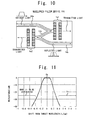
- Fig. 10 illustrates a wavelength filter device 101 in accordance with this embodiment.
- the incident light introduced through an optical waveguide path 14a is reflected into an optical waveguide path 14c, according to the reflection characteristics of a first-stage wavelength filter 1a1.
- This wavelength filter 1a1 includes the two lattice filters 2 of the first embodiment.
- the transmitted light that has been transmitted through the first-stage wavelength filter 1a1 is either absorbed by the wavelength filter device 101 or outputted.
- the light reflected into the optical waveguide path 14c is next reflected according to the reflection characteristics of a second-stage wavelength filter 1a2.
- the reflected light is then outputted through an optical waveguide path 14b.
- the wavelength filter 1a2 includes the two lattice filters 12 of the first embodiment.
- the transmitted light that has been transmitted through the second-stage wavelength filter 1a2 is either absorbed by the wavelength filter device 101 or outputted.
- Fig. 11 is a graph showing the reflection characteristics obtained by a calculation utilizing RCWA performed on the wavelength filter device 101 of this embodiment.
- two or more wavelength filters 1a are employed to sharply emphasize the boundaries between the reflection range and the attenuation range.
- the wavelengths outside the reflection range are further attenuated, so that the wavelength selectivity for the desired frequency band fb is improved, and that the attenuation rate in the frequency band to be attenuated is increased. Accordingly, the specific wavelength band normally required in optical communications is surely reflected, and the unnecessary frequency bands can be sufficiently attenuated.
- the other parts of the structure of this embodiment are the same as those of the first embodiment, and therefore, explanation of them is omitted in this description.
- wavelength filters 1a1 and 1a2 employed in the third embodiment may be replaced with wavelength filters 1b1 and 1b2 each including the three lattice filters 12 of the second embodiment.
- wavelength filters 1b1 and 1b2 each including the three lattice filters 12 of the second embodiment.
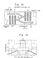
- Fig. 12 illustrates a wavelength filter device 102 of this embodiment.
- the incident light introduced through the optical waveguide path 14a is first reflected into the optical waveguide path 14c, according to the reflection characteristics of the first-stage wavelength filter 1b1.
- the wavelength filter 1b1 includes the three lattice filters 12 of the second embodiment.
- the transmitted light that has been transmitted through the first-stage wavelength filter 1b1 is either absorbed by the wavelength filter device 102 or outputted.
- the light reflected into the optical waveguide path 14c is next reflected according to the reflection characteristics of the second-stage wavelength filter 1b2.
- the reflected light is then transferred through the optical waveguide path 14b and outputted to the outside.
- the wavelength filter 1b2 includes the three lattice filters 12 of the second embodiment.
- the transmitted light that has been transmitted through the second-stage wavelength filter 1b2 is either absorbed by the wavelength filter device 102 or outputted.
- Fig. 13 is a graph showing the reflection characteristics obtained by a calculation utilizing RCWA performed on the wavelength filter device 102 of this embodiment.
- the two wavelength filters 1b1 and 1b2 sharply emphasize the boundaries between the reflection range and the attenuation range.
- the wavelengths outside the reflection range are further attenuated, so that the wavelength selectivity for the desired frequency band fb is improved, and that the attenuation rate in the frequency band to be attenuated is increased. Accordingly, the specific wavelength band normally required in optical communications is surely reflected, and the unnecessary frequency bands can be sufficiently attenuated.
- the other parts of the structure of this embodiment are the same as those of the first embodiment, and therefore, explanation of them is omitted in this description.
- the lattice filters 12 of each of the foregoing embodiments may be made of a material having an electrooptical effect, to thereby form a variable wavelength filter 2.
- this structure will be described as a fifth embodiment of the present invention.
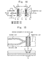
- Fig. 14 illustrates the structure of the variable wavelength filter 2 of this embodiment.
- the variable wavelength filter 2 includes two lattice filters 22.
- the number of lattice filters 12 is not limited to two, but may be three or greater.
- each of the lattice filters 22 has substances 22a and 22b alternately arranged in the direction perpendicular to the optical axis 10.
- ⁇ 1 represents the electrooptical constant of the substances 22a
- ⁇ 2 represents the electrooptical constant of the substances 22b.
- Examples of the materials for the substances 22a and 22b include LN (LiNbO 3 ), LT (LiTaO 3 ), PZT (Pb (Zr, Ti)O 3 ), and PLZT ((Pb, La) (Zr, Ti)O 3 ).
- Each of the lattice filters 22 also has electrodes 23 for inducing an electric field.
- the electrodes 23 are provided on the surfaces that reflect light and on the surfaces that transmit light. With this structure, an electric field can be induced in the lattice filters 22 made of a material having an electrooptical effect.
- each of the electrodes 23 is made of a material that is transparent to the target wavelength ⁇ 0 , such as ITO (indium-tin oxide).
- this embodiment achieves the same effects as each of the foregoing embodiments, and realizes the variable wavelength filter 2 that can vary the wavelength to be reflected according to the voltage to be applied to the electrodes 23. Accordingly, the wavelength selectivity can be diversified.
- the other parts of the structure of this embodiment are the same as those of the first embodiment, and therefore, explanation of them is omitted in this description.
- Each of the electrodes 23 can have a different structure from that of the fifth embodiment. In the following, such a case will be described as a sixth embodiment of the present invention.
- Fig. 15 illustrates an example of an optical device (a variable wavelength filter 200) using the variable wavelength filter 2.
- electrodes 24 are formed on planes that do not cross the optical axis 10, and are common to the two lattice filters 22. With this structure, an electric field can be induced in the lattice filters 22 made of a material having an electrooptical effect.
- the optical waveguide path 14 is directly connected to the lattice filters 22.
- one of the two electrodes 24 is provided on the back face of the LN substrate, opposite from the lattice filters 22.
- the arrangement of the electrodes 24 is not limited to this, but may be varied in many ways, as long as the two electrodes 24 can induce an electric field in the lattice filters 22.
- this embodiment can achieve the same effects as those of the fifth embodiment. Also, as the electrodes 24 are common to the two lattice filters 22, the production process can be simplified. The other parts of the structure of this embodiment are the same as those of the first embodiment, and therefore, explanation of them is omitted in this description.
- the substances 22a and 22b are both made of a material having an electrooptical effect in the fifth embodiment, it is also possible to form only the substances 22a or the substances 22b with a material having an electrooptical effect. In the following, such a case will be described as a seventh embodiment of the present invention.
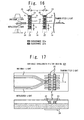
- Fig. 16 illustrates the structure of a variable wavelength filter 2a of this embodiment.
- electrodes 25 for inducing an electric field in the substances having electrooptical effects are provided only on the light reflection sides of the substances 22b.
- the electrodes 25 are also made of a material that is transparent to the target wavelength ⁇ 0 .
- this embodiment can provide a variable wavelength filter that avoids inducing an electric field in unnecessary substances. Accordingly, the wavelength selectivity can be further diversified.
- the other parts of the structure of this embodiment are the same as those of the first embodiment, and therefore, explanation of them is omitted in this description.
- An eighth embodiment of the present invention is to provide a structure in which a electrode 26 for inducing an electric field in either the substances 22a or 22b is provided for both of the two lattice filters 22, as shown in Fig. 17.
- this embodiment can provide a variable wavelength filter that avoids inducing an electric field in unnecessary substances. Also, as the electrodes 24 and 26 are common to the two lattice filters 22, the production process can be simplified. The other parts of the structure of this embodiment are the same as those of the first embodiment, and therefore, explanation of them is omitted in this description.
Landscapes
- Physics & Mathematics (AREA)
- General Physics & Mathematics (AREA)
- Optics & Photonics (AREA)
- Engineering & Computer Science (AREA)
- Microelectronics & Electronic Packaging (AREA)
- Optical Integrated Circuits (AREA)
- Optical Filters (AREA)
- Optical Modulation, Optical Deflection, Nonlinear Optics, Optical Demodulation, Optical Logic Elements (AREA)
Abstract
Description
Accordingly, the specific wavelength band normally required in optical communications is surely reflected, and the unnecessary frequency bands can be sufficiently attenuated. The other parts of the structure of this embodiment are the same as those of the first embodiment, and therefore, explanation of them is omitted in this description.
Claims (21)
- A wavelength filter comprising
a plurality of lattice structures that are arranged at predetermined intervals in the direction of an optical axis,
each of the lattice structures having regions of two different refractive indices that are alternately arranged. - The wavelength filter as claimed in claim 1, wherein the average refractive index of the lattice structures is higher than the refractive index of areas for transmitting light before and behind the lattice structures.
- The wavelength filter as claimed in claim 1 or 2, wherein the regions of two different refractive indices are alternately arranged in a direction perpendicular to the optical axis.
- The wavelength filter as claimed in any preceding claim, wherein the predetermined intervals are uniform.
- The wavelength filter as claimed in any preceding claim, wherein the lattice structures are formed on a substrate on which an optical waveguide path is also formed.
- The wavelength filter as claimed in any preceding claim, wherein the optical waveguide path is directly connected to the lattice structures.
- The wavelength filter as claimed in any preceding claim, wherein the optical waveguide path includes optical fibers.
- The wavelength filter as claimed in any preceding claim, comprising two or three of the lattice structures.
- A variable wavelength filter comprising
a plurality of lattice structures that are arranged at predetermined intervals in the direction of an optical axis,
each of the lattice structures having regions of two different substances that are alternately arranged, and
at least one of the substances being an electrooptical material. - The variable wavelength filter as claimed in claim 9, further comprising electrodes for inducing an electric field in the lattice structures.
- The variable wavelength filter as claimed in claim 9 or 10, wherein the average refractive index of the lattice structures is higher than the refractive index of areas for transmitting light before and behind the lattice structures.
- The variable wavelength filter as claimed in claim 9, 10 or 11, wherein the regions of two different substances are alternately arranged in a direction perpendicular to the optical axis.
- The variable wavelength filter as claimed in any one of claims 9 to 12, wherein the predetermined intervals are uniform.
- The variable wavelength filter as claimed in any one of claims 9 to 13, wherein the lattice structures are formed on a substrate on which an optical waveguide path is also formed.
- The variable wavelength filter as claimed in any one of claims 9 to 14, wherein the optical waveguide path is directly connected to the lattice structures.
- The variable wavelength filter as claimed in any one of claims 9 to 15, wherein the electrooptical material includes at least one of LiNbO3, LiTaO3, Pb(Zr, Ti)O3, and (Pb, La) (Zr, Ti)O3.
- The variable wavelength filter as claimed in claim 10, wherein the electrodes are formed on at least either the light reflection faces or the light transmission faces of the lattice structures.
- The variable wavelength filter as claimed in claim 17, wherein the electrodes are transparent electrodes.
- The variable wavelength filter as claimed in claim 10, 17 or 18, wherein the electrodes are common to two or more of the lattice structures.
- An optical device comprising one or more wavelength filters, each as claimed in any one of claims 1 to 8, or one or more variable wavelength filters, each as claimed in any one of claims 9 to 19, formed on a single substrate.
- An optical device as claimed in claim 20, having two or more such wavelength filters or two or more such variable wavelength filters formed on said single substrate, wherein the distance between the wavelength filters is longer than each of the predetermined intervals.
Applications Claiming Priority (2)
| Application Number | Priority Date | Filing Date | Title |
|---|---|---|---|
| JP2002215263A JP2004054181A (en) | 2002-07-24 | 2002-07-24 | Wavelength filter, variable wavelength filter, and optical element |
| JP2002215263 | 2002-07-24 |
Publications (2)
| Publication Number | Publication Date |
|---|---|
| EP1385031A2 true EP1385031A2 (en) | 2004-01-28 |
| EP1385031A3 EP1385031A3 (en) | 2004-10-13 |
Family
ID=29997248
Family Applications (1)
| Application Number | Title | Priority Date | Filing Date |
|---|---|---|---|
| EP03254464A Withdrawn EP1385031A3 (en) | 2002-07-24 | 2003-07-16 | Wavelength filter, variable wavelength filter, and optical device |
Country Status (5)
| Country | Link |
|---|---|
| US (1) | US20040017973A1 (en) |
| EP (1) | EP1385031A3 (en) |
| JP (1) | JP2004054181A (en) |
| KR (1) | KR20040010333A (en) |
| CN (1) | CN1480781A (en) |
Families Citing this family (5)
| Publication number | Priority date | Publication date | Assignee | Title |
|---|---|---|---|---|
| KR100873695B1 (en) * | 2007-08-03 | 2008-12-12 | 광주과학기술원 | Optical Filtering Method and System Using Titanium Diffused Lithium Naoate Waveguide |
| KR100971418B1 (en) * | 2007-10-29 | 2010-07-21 | 주식회사 메디슨 | Ultrasonic Diagnosis Device with Joystick |
| JP2015232599A (en) * | 2014-06-09 | 2015-12-24 | ソニー株式会社 | Optical filter, solid state image pickup device, and electronic apparatus |
| WO2016057339A1 (en) * | 2014-10-06 | 2016-04-14 | Go!Foton Holdings, Inc. | Apparatus and method for optical time-domain reflectometry |
| CN108627974A (en) * | 2017-03-15 | 2018-10-09 | 松下知识产权经营株式会社 | Photo-scanning system |
Family Cites Families (6)
| Publication number | Priority date | Publication date | Assignee | Title |
|---|---|---|---|---|
| US4508964A (en) * | 1982-09-29 | 1985-04-02 | Rockwell International Corporation | Electro-optically tuned rejection filter |
| DE3831905A1 (en) * | 1988-09-20 | 1990-03-22 | Standard Elektrik Lorenz Ag | OPTICAL WAVE MODULE WITH FIBER CONNECTOR |
| US5598300A (en) * | 1995-06-05 | 1997-01-28 | Board Of Regents, The University Of Texas System | Efficient bandpass reflection and transmission filters with low sidebands based on guided-mode resonance effects |
| US6035089A (en) * | 1997-06-11 | 2000-03-07 | Lockheed Martin Energy Research Corporation | Integrated narrowband optical filter based on embedded subwavelength resonant grating structures |
| US6212312B1 (en) * | 1999-09-17 | 2001-04-03 | U.T. Battelle, Llc | Optical multiplexer/demultiplexer using resonant grating filters |
| US6532326B1 (en) * | 2000-09-21 | 2003-03-11 | Ut-Battelle, Llc | Transverse-longitudinal integrated resonator |
-
2002
- 2002-07-24 JP JP2002215263A patent/JP2004054181A/en not_active Withdrawn
-
2003
- 2003-07-14 US US10/617,753 patent/US20040017973A1/en not_active Abandoned
- 2003-07-16 EP EP03254464A patent/EP1385031A3/en not_active Withdrawn
- 2003-07-23 KR KR1020030050429A patent/KR20040010333A/en not_active Withdrawn
- 2003-07-24 CN CNA031328806A patent/CN1480781A/en active Pending
Also Published As
| Publication number | Publication date |
|---|---|
| JP2004054181A (en) | 2004-02-19 |
| EP1385031A3 (en) | 2004-10-13 |
| KR20040010333A (en) | 2004-01-31 |
| CN1480781A (en) | 2004-03-10 |
| US20040017973A1 (en) | 2004-01-29 |
Similar Documents
| Publication | Publication Date | Title |
|---|---|---|
| US4296995A (en) | Optical fiber beam splitter couplers employing coatings with dichroic properties | |
| US6891992B2 (en) | Configurable add-drop filter utilizing chiral fiber gratings | |
| EP0347563B1 (en) | Bulk optic wavelength division multiplexer | |
| US6301042B1 (en) | Fabry-perot optical filter with chirped dielectric mirrors | |
| KR20110031379A (en) | How to employ a hybrid waveguide-mode resonant filter and distributed Bragg reflection | |
| AU3261301A (en) | Optical multiplexer/demultiplexer using resonant grating filters | |
| US6407863B1 (en) | Dual transmission band interference filter | |
| US4006964A (en) | Integrated optical waveguide having a filter | |
| JP2002169022A (en) | Optical element, spectroscopic device and integrated optical device using the same | |
| CN1292884A (en) | Tunable optical fiber bragg and long period grating | |
| EP1385031A2 (en) | Wavelength filter, variable wavelength filter, and optical device | |
| US7333266B2 (en) | CWDM filter | |
| CN1387627A (en) | Asymmetric low dispersion Bragg grating filter | |
| CN109164526A (en) | A kind of unpolarized type narrow-band optical bandpass filter | |
| US7355792B2 (en) | CWDM filter for eliminating noise | |
| KR100351562B1 (en) | Demultiplexer | |
| JP2001350040A (en) | Optical filter | |
| CN116381838B (en) | An angle-tunable nonpolarized narrowband optical bandpass filter | |
| JPH11326633A (en) | Wavelength selection element and optical device using the same | |
| Sinha et al. | Design of a thin-film-based optical filter for broadband multichannel communication systems | |
| JP2000214392A (en) | Optical wavelength filter | |
| JP2641238B2 (en) | Polarizer | |
| JPH10227942A (en) | High-speed continuous wavelength tunable filter | |
| SU1578676A1 (en) | Optical waveguide filter | |
| EP2071389A1 (en) | Acoustooptical filter |
Legal Events
| Date | Code | Title | Description |
|---|---|---|---|
| PUAI | Public reference made under article 153(3) epc to a published international application that has entered the european phase |
Free format text: ORIGINAL CODE: 0009012 |
|
| AK | Designated contracting states |
Kind code of ref document: A2 Designated state(s): AT BE BG CH CY CZ DE DK EE ES FI FR GB GR HU IE IT LI LU MC NL PT RO SE SI SK TR |
|
| AX | Request for extension of the european patent |
Extension state: AL LT LV MK |
|
| PUAL | Search report despatched |
Free format text: ORIGINAL CODE: 0009013 |
|
| AK | Designated contracting states |
Kind code of ref document: A3 Designated state(s): AT BE BG CH CY CZ DE DK EE ES FI FR GB GR HU IE IT LI LU MC NL PT RO SE SI SK TR |
|
| AX | Request for extension of the european patent |
Extension state: AL LT LV MK |
|
| RIC1 | Information provided on ipc code assigned before grant |
Ipc: 7G 02B 5/20 B Ipc: 7G 02B 6/12 B Ipc: 7G 02B 6/34 B Ipc: 7G 02B 6/293 A |
|
| AKX | Designation fees paid | ||
| REG | Reference to a national code |
Ref country code: DE Ref legal event code: 8566 |
|
| STAA | Information on the status of an ep patent application or granted ep patent |
Free format text: STATUS: THE APPLICATION IS DEEMED TO BE WITHDRAWN |
|
| 18D | Application deemed to be withdrawn |
Effective date: 20050414 |