Field of the Invention
-
The present invention relates to a process for
manufacturing an electrostatic chuck and a process for
manufacturing a ceramic heater, used mainly in the semiconductor
industry, particularly to: a process for manufacturing an
electrostatic chuck which does not have a dispersion in chucking
force; and a process for manufacturing a ceramic heater which
does not have a dispersion in calorific value.
Background Art
-
Semiconductors are very important products necessary in
various industries. A semiconductor chip is produced, for
example, by slicing a silicon monocrystal into a given thickness
to produce a silicon wafer, and then forming a plurality of
integrated circuits and the like on this silicon wafer.
-
In the process for producing this semiconductor chip, a
silicon wafer placed on an electrostatic chuck is subjected to
various treatments such as etching and CVD to form a conductor
circuit, an element and the like. At this time, corrosive gas
such as gas for deposition or gas for etching is used; therefore,
it is necessary to protect an electrostatic electrode layer from
corrosion by the gas. Also, since it is necessary to induce
adsorption power, the electrostatic electrode layer is usually
coated with a ceramic dielectric film or the like.
-
As this ceramic dielectric film, a nitride ceramic has
been conventionally used. For example, JP Kokai Hei 5-8140
discloses an electrostatic chuck, using a nitride such as
aluminum nitride. Further, in JP Kokai Hei 9-48668, a
carbon-containing aluminum nitride having an Al-O-N structure
is disclosed.
-
Furthermore, a process for manufacturing such an
electrostatic chuck is disclosed in JP Kokoku Hei 6-97677 and
the like.
-
Such an electrostatic chuckmade of ceramic is manufactured
by what is called a green sheet method wherein ceramic is produced
in the way that: a lamination is formed by stacking green sheets;
and then the lamination is sintered, as noted in JP Kokai Sho
62-264638, JP Kokai Sho 60-261377 and the like.
Summary of the Invention
-
However, electrostatic chucks using these ceramics have
a problem that chucking force thereof has a dispersion.
-
And further, ceramic heaters manufactured by the
above-mentioned green sheet method also have a
temperature-dispersion on the heating face.
-
The objective of the present invention is to reduce the
dispersion of chucking force and the temperature-difference on
the heating face of the electrostatic chuck and ceramic heater
(hot plate) manufactured by a green sheet method.
-
As a result of investigation of the reason of the
above-mentioned problem under the above-mentioned objective,
the inventors have found out that: unexpectedly, a problem exist
in a surface roughness of the green sheet used when a formed
body is produced; and, by setting the surface roughness thereof
to, as Rmax, 200µm or less, a dispersion of chucking force
depending on place of an electrostatic chuck is eliminated. Thus,
they have completed the present invention.
-
Inventors have also found out that by using such a green
sheet as a green sheet for a ceramic heater, they can produce
a ceramic heater wherein a dispersion of calorific value
depending on place of the resistance heating element does not
exist, and thus completed the present invention.
-
That is, a processfor manufacturing an electrostatic chuck
of the present invention comprises steps of:
- printing a conductor containing paste for an electrode
on a green sheet which has a surface roughness, Rmax, of 200
µm or less; forming a lamination by stacking another green sheet
or other green sheets on the above-mentioned green sheet; and
then sintering the lamination.
-
-
The electrostatic chuck manufactured in the present
invention is desirably in a disc shape having a diameter exceeding
150 mm.
-
Aprocess for manufacturing a ceramic heater of the present
invention comprises steps of:
- printing a conductor containing paste for a resistance
heating element on a green sheet which has a surface roughness,
Rmax, of 200 µm or less; forming a lamination by stacking another
green sheet or other green sheets on the above-mentioned green
sheet; and then sintering the above-mentioned lamination.
-
-
The ceramic heater manufactured in the present invention
is desirably in a disc shape having a diameter exceeding 150
mm.
Brief Description of the Drawings
-
- Fig.1 (a) to (d) are sectional views that schematically
illustrate a part of a process for manufacturing an electrostatic
chuck according to the present invention.
- Fig.2 is a sectional view that schematically illustrates
one example of an electrostatic chuck manufactured by the process
according to the present invention.
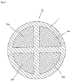
- Fig.3 is a sectional view taken along A-A line of the
electrostatic chuck illustrated in Fig. 2.
- Fig.4 is a sectional view taken along B-B line of the
electrostatic chuck illustrated in Fig. 2.
- Fig.5 is a sectional view that schematically illustrates
one example of an electrostatic chuck manufactured by the process
according to the present invention.
- Fig.6 is a sectional view that schematically illustrates
one example of an electrostatic chuck manufactured by the process
according to the present invention.
- Fig.7 is a sectional view that schematically illustrates
one example of an electrostatic chuck manufactured by the process
according to the present invention.
- Fig. 8 is a horizontal sectional view that schematically
illustrates a shape of an electrostatic electrode constituting
an electrostatic chuck manufactured by the process according
to the present invention.
- Fig. 9 is a horizontal sectional view that schematically
illustrates a shape of an electrostatic electrode constituting
an electrostatic chuck manufactured by the process according
to the present invention.
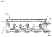
- Fig. 10 is a sectional view that schematically illustrates
the state that an electrostatic chuckmanufacturedby the process
according to the present invention is fitted into a supporting
case.
- Fig. 11 is a partially enlarged sectional view that
schematically illustrates a ceramic heater manufactured by the
process according to the present invention.
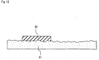
- Fig. 12 is a sectional view that schematically illustrates
a conductor containing paste layer formed on a produced green
sheet in a conventional process for manufacturing an
electrostatic chuck.
-
Explanation of symbols
-
- 1, 61
- ceramic substrate
- 2, 22, 32a, 32b
- chuck positive electrostatic layer
- 3, 23, 33a, 33b
- chuck negative electrostatic layer
- 2a, 3a
- semicircular part
- 2b, 3b
- comb-teeth-shaped part
- 4
- ceramic dielectric film
- 5, 12, 25, 62
- resistance heating element
- 6, 18, 63
- external terminal
- 7
- metal wire
- 8
- Peltier device
- 9
- silicon wafer
- 20, 30, 101, 201, 301, 401
- electrostatic chuck
- 16, 17, 69
- conductor-filled through hole
- 25a
- metal covering layer
- 35, 36
- blind hole
- 41
- supporting case
- 42
- coolant outlet
- 43
- inhalation duct
- 44
- coolant inlet
- 45
- heat insulator
- 50, 50'
- green sheet
- 51
- printed body for an electrostatic electrode
- 52
- printed body for a resistance heating element
- 53, 54
- printed body for a conductor filled through hole
- 60
- ceramic heater
- 61a
- heating face
- 61b
- bottom face
- 64
- bottomed hole
- 65
- through hole
Detailed Disclosure of the Invention
-
A process for manufacturing an electrostatic chuck of the
present invention comprises steps of:
- printing a conductor containing paste for an electrode
on a green sheet which has a surface roughness, Rmax, of 200
µm or less; forming a lamination by stacking another green sheet
or.other green sheets on the above-mentioned green sheet; and
then sintering the above-mentioned lamination.
-
-
In the conventional process for manufacturing the
electrostatic chuck, such a green sheet 91 having a large
unevenness of the surface roughness, Rmax, exceeding 200 µm was
used and a conductor containing paste layer 92 was occasionally
formed on the green sheet 91 as shown in Fig. 12. In this case,
the formed conductor containing paste layer 92 has a various
thickness depending on place, therefore, resultantly, the
produced electrostatic electrode of electrostatic chuck has
unevenness in the thickness thereof.
As a result, a dispersion of chucking force depending on place
was caused.
-
Also, unevenness was produced in a resistance heating
element for a heater, thus, various calorific value depending
on place were producing the temperature-differenceonthe heating
face.
-
Such a tendency is especially significant in the
disc-shaped body having a diameter exceeding 150mm. It is
presumed that: at the time when JP Kokai Sho 62-264638 and JP
Kokai Sho 60-261377 were filed, the market only demanded the
one having a small diameter of about 150mm, hence, the dispersion
of the chucking force and the temperature-difference of the
heating face thereof hardly became problems.
-
However, in the present invention, since so much attention
is paid on a surface roughness of the green sheet and thus
relatively flat green sheet which has a surface roughness, Rmax,
of 200µm or less is used, the conductor containing paste layer
formed thereon has even thickness without a dispersion depending
on place. Accordingly, the produced electrostatic electrode
of the electrostatic chuck does not have unevenness on the
thickness thereof so that the electrostatic chuck wherein an
electrostatic electrode as a whole has even chucking force can
be produced.
-
Also, the dispersion in the thickness of the resistance
heating element can be made small so that the resistance value
becomes constant, thus making the temperature difference on the
heating face small as a whole.
-
The unevenness of the chucking force of the above-mentioned
electrostatic chuck depending on place can be evaluated by
measuring the surface temperature of the adsorbed semiconductor
wafer by the thermoviewer. This is because: if the semiconductor
wafer is adsorbed strongly to the adsorbing face of the
electrostatic chuck, the temperature thereof becomes high and
accordingly the dispersion of the chucking force is reflected
on the temperature distribution.
-
Also, it is possible to measure the dispersion thereof
by: putting a semiconductor wafer divided in a plurality of parts
thereon; and measuring the adsorption force of each divided part
by a load cell. In the Examples describedbelow, both the methods
mentioned above were employed.
-
A surface roughness, Rmax, of a green sheet can be
controlled either :by adjusting a particle diameter of the raw
material ceramic powder to a given extent; by adjusting the
viscosity of the composition for a green sheet to a given extent
at the time of preparing thereof; or by selecting the drying
condition. The condition for those is explained in detail in
the part of an embodiment of the invention described below.
-
A process for manufacturing a ceramic heater of the present
invention comprises steps of:
- printing a conductor containing paste for a resistance
heating element on a green sheet which has a surface roughness,
Rmax, of 200 µm or less; forming a lamination by stacking another
green sheet or other green sheets on the above-mentioned green
sheet; and then sintering the above-mentioned lamination.
-
-
Accordingly, a resistance heating element produced by the
above-mentioned process for a ceramic heater also has even
thickness without dispersion depending on place, thus it
generates even heat. Hence, the temperature of the face (heating
face) of the ceramic heater for heating an object to be heated
such as a semiconductor wafer becomes uniform so that an object
to be heated can be heated evenly.
-
Similarly to the above-mentioned process for
manufacturing an electrostatic chuck, a surface roughness Rmax
of a green sheet can be controlled either : by adj usting a particle
diameter of the raw material ceramic powder to a given extent;
by adjusting the viscosity of the composition for a green sheet
to a given extent at the time of preparing thereof ; or by selecting
the drying condition.
-
Likewise, the unevenness of the calorific value of the
above-mentioned resistance heating element depending on place
can be evaluated by measuring the surface temperature of the
semiconductor wafer placed on a heating face by the thermoviewer.
This is because: the dispersion of calorific value depending
on the portion is also reflected on the temperature-distribution
of the heating face.
-
In this case, measurement can be done by observing the
temperature distribution of the semiconductor wafer in the
condition that disposing only resistance heating elements in
the ceramic substrate.
-
A process for manufacturing an electrostatic chuck and
a process for manufacturing a ceramic heater of the present
invention are the same in that: in each process, after a green
sheet is formed, a conductor containing paste is printed on the
green sheet, then, after forming a lamination by stacking another
green sheet or other green sheets on the thus produced green
sheet which has a conductor containing paste layer, the
lamination is sintered. And the difference only exists in the
shape or the like of the conductor containing paste formed on
the green sheet. Therefore, hereinafter, a process for
manufacturing an electrostatic chuck is mainly explained and
a process for manufacturing a ceramic heater is explained by
complementing it.
-
A process for manufacturing an electrostatic chuck of the
present invention comprises steps of:
- printing a conductor containing paste for an electrode
on a green sheet which has a surface roughness, Rmax of 200
µm or less; forming a lamination by stacking another green sheet
or other green sheets on the above-mentioned green sheet; and
then sintering the above-mentioned lamination.
-
-
Fig.1 (a) to (d) are sectional views that schematically
illustrate one example of a process for manufacturing an
electrostatic chuck according to the present invention.
- (1) In the present invention, firstly, by mixing raw material
powder of ceramic such as a nitride ceramic or a carbide ceramic,
with a binder and a solvent, a green sheet 50 having a surface
roughness, as Rmax, of 200 µm or less is formed.
The reason why the surface roughness of the green sheet
is adjusted to be 200 µm or less is that: if the roughness, as
Rmax, exceeds 200 µm, the surface of the green sheet is too coarse
so that unevenness is formed on the portion of a conductor
containing paste contacting with the green sheet, thus the
thickness of an electrostatic electrode layerof themanufactured
electrostatic chuck is dispersed depending on place, as a result
of that, a chucking force thereof is also dispersed. Incidentally,
needless to say the surface roughness Rmax of the green sheet
does not exceed the thickness of the green sheet. Taking the
strength of the green sheet into consideration, the surface
roughness Rmax of the green sheet does not exceed 2/3 of the
thickness of the green sheet. To be specific, the surface
roughness Rmax of the green sheet is desirably 0.1µm or more
and less than 50µm.The ceramic material constituting the electrostatic chuck
which is an obj ect to be manufactured is not specifically limited
and examples thereof include, for example, a nitride ceramic,
a carbide ceramic, an oxide ceramic and the like.Examples of the above-mentioned nitride ceramic are metal
nitride ceramic such as, for example, aluminum nitride, silicon
nitride, boron nitride, and the like.Also, examples of the above-mentioned carbide ceramic are
metal carbide ceramic such as, for example, silicon carbide,
zirconium carbide, tantalum carbide, tungsten carbide, and the
like.The examples of the above-mentioned oxide ceramic are a
metal oxide ceramic such as alumina, zirconia, cordierite,
mullite, beryllia and the like.These ceramics may be used either alone or in combination
of two or more kinds of them.Among these ceramics, nitride ceramic and oxide ceramic
are preferred.Aluminum nitride is most preferable among those nitride
ceramics. That is because the produced ceramic substrate has
the highest thermal conductivity of 180 W/m•K.The raw material powder of ceramic can be, for instance,
aluminum nitride powder formed with a layer of an oxide on its
surface by firing it in the oxidative atmosphere or the like.Also, based on the necessity, a sintering aid such as yttria,
alumina and sulfur compounds, and a catalyst can be added. The
average particle diameter of the material powder is preferably
0.1 to 5µm.Since several or one green sheet(s) 50' laminated on a
green sheet on which an electrostatic electrode layer printed
body 51 is formed become/becomes a layer to be the ceramic
dielectric film 4, if necessary, it may have a composition
different from that of the ceramic substrate.But, normally, as the raw materials of the ceramic
dielectric film 4, it is preferable to use the same material
as that of the ceramic substrate 1. That is because they are
integrated and sintered together in many cases and thus, the
firing conditions are the same. However, in case where the
materials are different, it may be possible: to produce the
ceramic substrate at first; and to form a conductor containing
paste layer which is to be an electrostatic electrode layer
thereon; then to form a green sheet which is to be a ceramic
dielectric film further thereon; and finally to sinter it.As the binder, at least one selected from acrylic binder,
ethyl cellulose, butyl cellosolve, polyvinyl alcohol is
desirable.In addition, as the solvent, at least one selected from
α-terpineol and glycol is desirable.The paste obtained by mixing them is formed to be a
sheet-like shape by a forming method such as doctor blade method
to produce the green sheet 50. At this time, the viscosity of
the green sheet before drying is preferably 1×10⁴ to 4×10⁴ cP
(10 to 40 Pa • s). By adjusting the viscosity of the green sheet
in this extent, the unevenness on the green sheet becomes small,
thus making the surface roughness, Rmax, to 200 µm or less.If the viscosity of the green sheet is less than 1×10⁴
cP (10 Pa • s), fluidity is too large to maintain the shape of
the green sheet. Whereas, if the viscosity of the green sheet
exceeds 4×10⁴ cP (40 Pa•s), it becomes difficult to flatten
the surface of the green sheet by using a blade and the like,
and in some cases, the surface roughness thereof, Rmax, exceeds
200 µm.The easiest method to adjust the surface roughness of the
green sheet is to select the drying condition. In case that the
viscosity of the green sheet is 1×10⁴ to 4×10⁴ cP (10 to 40 Pa •
s), drying is conducted at 50 to 200 °C for 10 to 60 minutes.
In this process, by setting the initial temperature for drying
to less than 150°C, the surface roughness, Rmax, can be adjusted
to 200 µm or less. Specifically, if the drying is conducted at
high temperature, the solvent and the like existing inside
volatilize rapidly thus making the surface thereof coarse, and
if the drying is conducted at low temperature, the surface thereof
becomes smooth. Incidentally, JP Kokai Hei 12-21961 specified
a process of manufacturing an electrostatic chuck by green sheet
method. But, the viscosity of the green sheet is not specified.
Therefore, with such publications, patentability of the present
invention can never be affected.Next, if necessary, the following may be provided in the
green sheet 50: through holes for letting lifter pins of the
silicon wafer pass through; a concave portion for embedding the
thermocouple; and a part where the conductor-filled through holes
are formed. The through holes can be formed by punching and
the like.These through holes and concave portions and the like can
be formed by drilling and the like, either: after forming a green
sheet lamination; or after forming a sintered body.The preferable thickness of the green sheet 50 is
approximately 0.1 to 5 mm.Next, the through holes of the green sheet 50 are filled
with the conductor containing paste to obtain conductor-filled
through hole printed bodies 53, 54 and then the conductor
containing paste to be the electrostatic electrode layers and
resistance heating elements are printed on the green sheet 50.The printing is carried out so as to obtain a desired aspect
ratio in consideration of the shrinkage ratio of the green sheet
50, thereby obtaining an electrostatic electrode layer printed
body 51 and a resistance heating element printed body 52.The printed bodies are formed by printing conductor
containing pastes containing conductive ceramics, metal
particles and the like. As the shape of the electrostatic
electrode layer, the shapes illustrated on Fig. 3, Fig. 8 and Fig. 9
are listed. The resistance heating element will be explained
later.As the conductive ceramic particles contained in these
conductor containing pastes, a carbide of: tungsten; or
molybdenum is optimum. That is because they are hardly oxidized
and their thermal conductivity are hard to be lowered.Asthe metal particles,for example, tungsten, molybdenum,
platinum, nickel and the like can be used.The average particle diameter of the conductive ceramic
particles and the metal particles is preferably 0.1 to 5 µm.
That is because the conductor containing paste is difficult to
be printed if the size is too large or too small.As such a paste, the conductor containing paste produced
by the following is optimum; mixing 85 to 97 parts by weight
of metal particles or conductive ceramic particles, 1.5 to 10
parts by weight of at least one binder selected from an acrylic
type binder, ethyl cellulose, butyl cellosolve, and polyvinyl
alcohol, and 1.5 to 10 parts by weight of at least one solvent
selected from α-terpineol, glycol, ethyl alcohol and butanol.
In this case, the viscosity of the arranged conductor containing
paste is preferably 5×10⁴ to 50×104 cP (50 to 500 Pa • s). Next, as shown in Fig. 1(a), the green sheet 50 having
the printed bodies 51, 52, 53, 54 and the green sheet 50' having
no printed body are laminated. The reason why the green sheet
50' having no printed body is laminated on the resistance heating
element formation side is to prevent the end surfaces of the
conductor-filled through holes from being exposed and oxidized
at the time of firing of the resistance heating element formation.
If firing for the resistance heating elements formation is
carried out with the end faces of the conductor-filled through
holes exposed, it is required that the sputtering of
non-oxidizable metal such as nickel is conducted. Also,
covering with a gold brazing material of Au-Ni may be carried
out.
- (2) Next, as shown in Fig. 1(b), the lamination is heated
and pressurized to form the lamination of the green sheets. The
heating temperature of the lamination is preferably 50 to 300
°C and the pressure is preferably 20 to 200 kg /cm2.
Following this, the green sheets and the conductor
containing pastes are sintered. The heating temperature at the
firing is preferably 1000 to 2000 °C and the pressure at the
firing is preferably 100 to 200 kg /cm2. The heating and
pressuring are carried out under the inert gas atmosphere. As
the inert gas, argon, nitrogen and the like can be used. In
the firing step, conductor-filled through holes 16, 17, the chuck
positive electrostatic layer2,the chuck negative electrostatic
layer 3, resistance heating elements 5 and the like are formed.After producing the ceramic substrate by the
above-mentionedmethod, annealingcanbeconductedontheceramic
substrate at 1400 to 2000 °C. By this procedure, impurities such
as oxygen contained in grains of the crystal are discharged to
the out of the crystal, and the thermal conductivity is improved.
- (3) Next, as shown in Fig. 1(c), blind holes 35, 36 for
external terminals connection are formed.
Inner walls of the blind holes 35, 36 are preferably at
least partially made conductive and the inner walls, thus made
conductive, are preferably connected with the chuck positive
electrostatic layer 2, the chuck negative electrostatic layer
3, resistance heating elements 5 and the like.
- (4) Finally, as shown in Fig. 1(d), external terminals
6 , 18 are disposed in the blind holes 35, 36 through a gold brazing
material. In addition, if necessary, a bottomed hole may be
formed to bury a thermocouple inside thereof.
-
-
As a solder, alloys of silver-lead, lead-tin, bismuth-tin
and the like can be used. Still more, the thickness of the solder
layer is preferably 0.1 to 50 µm. That is because this range
is sufficient to keep the connection by the solder.
-
By adopting such a manufacturing process, for instance,
an electrostatic chuck illustrated in Figs.2,3 can be produced.
The electrostatic electrode layer of the obtained electrostatic
chuck does not have thickness dispersion so that an electrostatic
chuck has even chucking force as a whole.
-
Fig. 2 is a vertical sectional view that schematically
illustrates one embodiment of an electrostatic chuck
manufactured by the above-mentioned process. Fig. 3 is a
sectional view taken along the A-A line of the electrostatic
chuck shown in Fig. 1. Fig. 3 is a sectional view taken along
the B-B line of the electrostatic chuck shown in Fig. 2.
-
In this electrostatic chuck 101, an electrostatic
electrode layer composed of a chuck positive electrostatic layer
2 and a chuck negative electrostatic layer 3 is formed inside
a ceramic substrate 1 in a circular shape. A thin ceramic layer
4 (hereinafter, referred to as a ceramic dielectric film) is
formed on this electrostatic electrode layer. Also, a silicon
wafer 9 is placed on the electrostatic chuck 101 and is earthed.
-
As shown in Fig. 3, the chuck positive electrostatic layer
2 is composed of a semicircular arc part 2a and a comb-teeth-shaped
part 2b. The chuck negative electrostatic layer 3 is also
composed of a semicircular arc part 3a and a comb-teeth-shaped
part-3b. These chuck positive electrostatic layer 2 and chuck
negative electrostatic layer 3 are arranged face-to-face in such
a manner that the teeth of one comb-teeth-shaped part 2b extend
in staggered relation with the teeth of the other
comb-teeth-shaped part 3b. The + side and the - side of a direct
current power source are connected to the chuck positive
electrostatic layer 2 and chuck negative electrostatic layer
3, respectively. Thus, a direct current V2 is to be applied
thereto.
-
In order to control the temperature of the silicon wafer
9 , resistance heating elements 5 in the form of concentric circles
as viewed from the above, as shown in Fig. 4, are set up inside
the ceramic substrate 1. External terminals 6 are connected
and fixed to both ends of the resistance heating elements 5,
and a voltage V1 is to be applied thereto. Bottomed holes 11
for inserting temperature-measuring elements and through holes
12 for letting lifter pins (not illustrated) that support the
silicon wafer 9 and move it up and down pass through are formed
in the ceramic substrate 1, as shown in Fig. 4 but not shown
in Figs. 2. Incidentally, the resistance heating elements 5
may be formed on the bottom face of the ceramic substrate 1.
-
When this electrostatic chuck 101 is caused to function,
a direct voltage V2 is applied to the chuck positive electrostatic
layer 2 and the chuck negative electrostatic layer 3. In this
way, the silicon wafer 9 is adsorbed and fixed to the chuck positive
electrostatic layer 2 and the chuck negative electrostatic layer
3 through the ceramic dielectric film 4 by electrostatic action
of these electrodes. The silicon wafer 9 is fixed onto the
electrostatic chuck 101 in this way, and subsequently the silicon
wafer 9 is subjected to various treatments such as CVD and the
like.
-
Next, a ceramic substrate constituting an electrostatic
chuck manufactured by the above-mentioned process will be
explained. The ceramic substrate means the parts other than
ceramic dielectric film, in this electrostatic chuck.
-
The above-mentioned electrostatic chuck is preferably
used at 150 °C or higher, most preferably at 200 °C or higher.
-
In the above-mentioned ceramic substrate, it is desirable
that the pore diameter of the maximum pore is 50 µm or less and
the porosity thereof is 5% or less. Also, in the above-mentioned
ceramic substrate, it is desirable that there are no pores, or
even if there are pores, the pore diameter of the largest pore
is 50 µm or less.
-
If there are no pores, breakdown voltage at high
temperature becomes particularly high. To the contrary, if the
pores exist to some extent, fracture toughness value becomes
higher. Hence, which design to take will be decided based on
the required characteristics.
-
The reason why fracture toughness value is improved by
the existence of the pores is not clear. However, it is presumed
that the development of the cracks is stopped by the pores.
-
The reason why the pore diameter of the maximum pore is
desirably 50 µm or less is that: if the pore diameter is over
50 µm, high breakdown voltage property cannot be ensured at a
high temperature, particularly at 200 °C or higher.
-
The pore diameter of the maximum pore is desirably 10 µm
or less. This is because a degree of a warp at 200 °C or higher
becomes small.
-
The porosity and the pore diameter of the maximum pore
can be adjusted by pressing time, pressure, temperature at the
time of sintering, and additives such as SiC and BN. As mentioned
above, since SiC and BN obstruct sintering, pores can be
introduced by them.
-
At the measurement of the pore diameter of the maximum
pore, 5 samples are prepared. The surfaces thereof are ground
into mirror planes. With an electron microscope, ten points
on the surface are photographed with 2000 to 5000 magnifications.
The maximum pore diameters are selected from the photographs
obtained by the photographing, and the average of the 50 shots
is defined as the pore diameter of the maximum pore.
-
The porosity is measured by Archimedes' method.
According to this method, a sintered body is crushed into pieces,
and the crushed pieces are put into an organic solvent or mercury
to measure the volume thereof. Then the true specific gravity
of the pieces is obtained from the weight and the measured volume
thereof, and the porosity is calculated from the true specific
gravity and apparent specific gravity.
-
The diameter of the above-mentioned ceramic substrate
desirably exceeds 150mm, and is more desirably 200 mm or more.
It is particularly desirable that the diameter is 12 inches (300
mm) or more.
-
This is because in a large substrate having a diameter
exceeding 150mm, the dispersion of the temperature of a heated
semiconductor wafer will be large attributed to the dispersion
of the chucking force. Also, the thermal capacity of the ceramic
substrate becomes large and the temperature of the heating face
becomes uneven. To say conversely, in a ceramic substrate with
diameter of some 150mm, even though chucking force is dispersed
to some extent, the surface temperature becomes even, since the
semiconductor wafer is also small. Further, if the resistance
value of the resistance heating element is dispersed to some
extent, the temperature thereof easily rises and tend to be
relatively even, since the thermal capacity of the ceramic
substrate is small.
-
Incidentally, in the example of the publication of JP Kokai
Hei 11-74064, the ceramic substrate having a diameter of 300mm
is disclosed. However, the electrode is not the one formed by
performing printing on the green sheet, hence the existence of
such a reference never affect the patentability of the present
invention.
-
The thickness of the above-mentioned ceramic substrate
is desirably 50 mm or less, and particularly desirably 25 mm
or less.
-
If the thickness of the ceramic substrate is over 25 mm,
the thermal capacity of the ceramic substrate may be too large
in some cases. Particularly when a temperature controlling
means is set up to heat or cool the substrate,
temperature-following property may become poor due to the large
thermal capacity.
-
The thickness of the ceramic substrate is optimally
exceeding 1.5mm, and 5 mm or less.
-
In cases that the thickness of the substrate is 1.5mm or
less, the large ceramic substrate with a diameter exceeding 150
mm causes a large degree of amount of warp and thus not practical.
-
The above-mentioned ceramic substrate desirably contains
oxygen in an amount of 0.05 to 10% by weight. This is because,
by segregating oxygen to grain boundary, it becomes possible
to improve fracture toughness value.
-
If the oxygen content is below 0.05% by weight, the
sintering does not proceed enough and thus porosity becomes high
and thermal conductivity becomes low. To the contrary, if the
oxygen content exceeds 10% by weight, the amount of oxygen in
grain boundaries becomes too large and thus thermal conductivity
drops with a consequent deterioration of the temperature-rising
and temperature-dropping property.
-
In order to incorporate oxygen in the above-mentioned
ceramic substrate, as mentioned above, the firing of the material
powder is conducted in oxidative atmosphere or a metal oxide
may be added in the material powder.
-
Examples of the above-mentionedmetal oxide include yttria
(Y2O3), alumina (Al2O3) , rubidium oxide (Rb2O), lithium oxide
(Li2O), calcium oxide (CaCO3) and the like.
-
The content of these metal oxides is preferably 0.1 to
20 % by weight.
-
In the present invention, the ceramic substrate desirably
contains 5 to 5000 ppm of carbon.
-
The ceramic substrate can be blackened by incorporating
carbon and thus, when the substrate is used as a heater, radiant
heat can be sufficiently used.
-
Carbon may be amorphous or crystalline. When amorphous
carbon is used, a drop in the volume resistivity at high
temperature can be prevented. And when crystalline carbon is
used, a drop in the thermal conductivity at high temperature
can be prevented. Therefore, crystalline carbon and amorphous
carbon may be used together dependently on the purpose. The
carbon content is preferably from 50 to 2000 ppm.
-
When carbon is contained in the ceramic substrate, carbon
is preferably contained in the manner that its brightness will
be N6 or less as a value based on the rule of JIS Z 8721. The
ceramic having such brightness is superior in radiant heat
capacity and concealing property.
-
The brightness N is defined as follows: the brightness
of ideal black is made to 0; that of ideal white is made to 10;
respective colors are divided into 10 parts in the manner that
the brightness of the respective colors is recognized stepwise
between the brightness of black and that of white at equal
intensity intervals; and the resultant parts are indicated by
symbols N0 to N10, respectively.
-
Actual brightness is measured by comparison with color
chips corresponding to N0 to N10. One place of decimals in this
case is made to 0 or 5.
-
The material of the ceramic dielectric film constituting
the above-mentioned electrostatic chuck is not especially
limited, and examples thereof include a nitride ceramic, a
carbide ceramic, an oxide ceramic, and the like. Among them,
a nitride ceramic is most preferable.
-
As the above-mentioned nitride ceramic, the same as the
above-mentioned ceramic substrate can be listed. However, it
is preferable that a nitride ceramic is containing oxygen.
-
For example, raw material powder of the nitride ceramic
is heated in an oxidative atmosphere or in the air, or the raw
material powder of the nitride ceramic is mixed with a metal
oxide and then the mixture is sintered, in order to incorporate
oxygen into the above-mentioned nitride ceramic.
-
Examples of the above-mentioned metal oxide include
alumina (Al2O3), silicon oxide (SiO2), and the like.
-
The amount to be added of these metal oxides is preferably
0.1 to 10 parts by weight per 100 parts by weight of the nitride
ceramic.
-
By adjusting the thickness of the ceramic dielectric film
to 50 to 5000 µm, sufficient breakdown voltage can be secured
without lowering chucking force.
-
If the thickness of the above-mentioned ceramic dielectric
film is below 50 µm, the film thickness is too thin to obtain
sufficient breakdown voltage. Thus, when a silicon wafer is
placed on the film and is adsorbed thereon, the ceramic dielectric
film may undergo dielectric breakdown. On the other hand, if
the thickness of the above-mentioned ceramic dielectric film
is over 5000 µm, the distance between the silicon wafer and the
electrostatic electrodes becomes large so that the capability
of adsorbing the silicon wafer becomes poor. The thickness of
the ceramic dielectric film is preferably 100 to 1500 µm.
-
In the electrostatic chuck 101, the ceramic dielectric
film 4 is made of a nitride ceramic containing oxygen. Also,
it is desirable that its porosity is 5% or less, and the pore
diameter of its maximum pore is 50 µm or less. Also, the pores
in this dielectric film 4 are preferably composed of pores
independent each other.
-
In the ceramic dielectric film 4 having such a constitution,
it does not happen that gas and the like which cause a drop in
the breakdown voltage penetrate through the ceramic dielectric
film to corrode the electrostatic electrode and lower the
breakdown voltage of the ceramic dielectric film even at high
temperature.
-
If the above-mentioned porosity is over 5%, the number
of the pores increases and the pore diameter becomes too large.
As a result, the pores interconnect easily with each other. In
the ceramic dielectric film having such a structure, the
breakdown voltage drops.
-
If the pore diameter of the maximum pore is over 50 µm,
the sufficient breakdown voltage cannot be maintained at high
temperature even if the oxide is present in the boundaries between
the particles. In the case that the pores are present, the
porosity is more preferably 0.01 to 3% and the pore diameter
of the maximum pore is more preferably 0.1 to 10 µm.
-
The ceramic dielectric film desirably contains 50 to 5000
ppm of carbon. This is because the electrode pattern set inside
the electrostatic chuck can be concealed and high radiant heat
can be obtained. Also, the volume resistivity becomes lower,
the capability of adsorbing a silicon wafer becomes high at low
temperature.
-
The reason why in the electrostatic chuck of the present
invention a considerable number of the pores may be present in
the ceramic dielectric film is that the pores can cause an
improvement in the fracture toughness value and the resistance
to thermal impact.
-
Figs. 8, 9 are horizontal sectional views, each of which
schematically shows an electrostatic electrode in another
electrostatic chuck. In an electrostatic chuck 20 shown in Fig.
8, a chuck positive electrostatic layer 22 and a chuck negative
electrostatic layer 23 in a semicircular shape are formed inside
a ceramic substrate 1. In an electrostatic chuck shown in Fig.
9, chuck positive electrostatic layers 32a and 32b and chuck
negative electrostatic layers 33a and 33b, each of which has
a shape obtained by dividing a circle into 4 parts, are formed
inside a ceramic substrate 1. The two chuck positive
electrostatic layers 22a, 22b and the two chuck negative
electrostatic layers 33a, 33b are formed to cross, respectively.
-
In the case that an electrode having a form that an electrode
in the shape of a circle or the like is divided is formed, the
number of divided pieces is not particularly limited and may
be 5 or more. Its shape is not limited to a sector, either.
-
Examples of the electrostatic chuck according to the
present invention include: the electrostatic chuck 101 having
a structure wherein the chuck positive electrostatic layer 2
and the chuck negative electrostatic layer 3 are arranged between
the ceramic substrate 1 and the ceramic dielectric film 4 and
the resistance heating elements 5 are set up inside the ceramic
substrate 1, as shown in Fig. 2; the electrostatic chuck 201
havinga structure wherein the chuckpositive electrostatic layer
2 and the chuck negative electrostatic layer 3 are arranged
between the ceramic substrate 1 and the ceramic dielectric film
4 and the resistance heating elements 25 are disposed on the
bottom face of the ceramic substrate 1, as shown in Fig. 5; the
electrostatic chuck 301 having a structure wherein the chuck
positive electrostatic layer 2 and the chuck negative
electrostatic layer 3 are arranged between the ceramic substrate
1 and the ceramic dielectric film 4 and the metal wire 7, which
is a resistance heating element, is embedded in the ceramic
substrate 1, as shown in Fig. 6; and the electrostatic chuck
401 having a structure wherein the chuck positive electrostatic
layer 2 and the chuck negative electrostatic layer 3 are arranged
between the ceramic substrate 1 and the ceramic dielectric film
4 and the Peltier device 8 composed of the thermoelectric element
81 and the ceramic plate 82 is formed on the bottom face of the
ceramic substrate 1, as shown in Fig. 7.
-
As the electrostatic chuck shown in Fig. 7, in the case
that the Peltier device is used as the temperature controlling
means, both heating and cooling can be attained by changing the
direction along which an electric current passes. Thus, this
case is advantageous.
-
The Peltier device 8 is formed by connecting p type and
n type thermoelectric elements 81 in series and then jointing
the resultant to a ceramic plate 82 and the like.
-
Examples of the Peltier device include silicon/germanium,
bismuth/antimony, lead/tellurium type materials, and the like.
-
As shown in Figs. 2 to 7, in the above-mentioned
electrostatic chuck, the chuck positive electrostatic layer 2
and the chuck negative electrostatic layer 3 are arranged between
the ceramic substrate 1 and the ceramic dielectric film 4 and
the resistance heating element 5 or the metal wire 7 is formed
inside the ceramic substrate 1. Therefore, connecting units
(conductor-filled through holes) 16,17 are necessary for
connecting these to external terminals.
-
The conductor-filled through holes 16,17 are made by
filling there with a high melting point metal such as tungsten
paste or molybdenum paste, or a conductive ceramic such as
tungsten carbide or molybdenum carbide.
-
The diameter of the connecting portions (conductor-filled
through holes) 16,17 is desirably from 0.1 to 10 mm. This is
because disconnection can be prevented and further cracks or
strains can be prevented.
-
The conductor-filled through holes are used as connecting
pads to connect with external terminals 6,18 (reference to Fig.
1(d)).
-
The connecting thereof is performed with solder or brazing
material. As the brazing material, brazing silver, brazing
palladium, brazing aluminum, or brazing gold is used. Brazing
gold is desirably Au-Ni alloy. This is because Au-Ni alloy is
superior in adhesiveness to tungsten.
-
The ratio of Au/Ni is desirably [81.5 to 82.5 (% by
weight)]/[18.5 to 17.5 (% by weight)].
-
The thickness of the Au-Ni layer is desirably from 0.1
to 50 µm. This is because this range is sufficient for securing
connection. If Au-Cu alloy is used at a high temperature of
500 to 1000 °C and at a high vacuum of 10-6 to 10-5 Pa, the Au-Cu
alloy deteriorates. However, Au-Ni alloy does not cause such
deterioration and is profitable. Also, when the total amount
of the Au-Ni alloy is regarded as 100 parts by weight, the amount
of impurities therein is desirably below 1 part by weight.
-
If necessary, in the present invention a thermocouple may
be buried in the bottomed hole in the ceramic substrate. This
is because the thermocouple makes it possible to measure the
temperature of the resistance heating element and, on the basis
of the resultant data, voltage or electric current is changed
so that the temperature can be controlled.
-
The size of the connecting portion of metal wires of the
thermocouple is desirably the same as the strand diameter of
the respective metal wires or larger, and is preferably 0.5 mm
or less. Such a structure makes the thermal capacity of the
connecting portion small, and causes a temperature to be
correctly and rapidly converted to a current value. For this
reason, temperature controllability is improved so that the
temperature distribution of the heated surface of the
semiconductor wafer becomes small.
-
Examples of the above-mentioned thermocouple include K,
R, B, S, E, J and T type thermocouples, described in JIS-C-1602
(1980).
-
In the above-mentioned manufacturing method of an
electrostatic chuck, the electrostatic chuck 101 (reference to
Fig. 2, 3) is given as an example. In the case that the
electrostatic chuck 201 (reference to Fig. 5) is produced, it
is advisable to: produce a ceramic substrate having an
electrostatic electrode layer first; then print a conductor
containing paste on the bottom face of this ceramic substrate
and sinter the resultant to form the resistance heating elements
25; and then form the metal covering layer 25a by electroless
plating and the like. In the case that the electrostatic chuck
301 (reference to Fig. 6) is produced, it is advisable that:
firstly, a metal wire is placed on the green sheet instead of
forming a conductor containing paste layer which is to be a
resistance heating element, and other than that, almost the same
process as in the case of the electrostatic chuck 101 can be
adopted.
-
Further, in the case that the electrostatic chuck 401
(reference to Fig. 7) is produced, it is advisable that: firstly
a ceramic substrate having an electrostatic electrode layer is
produced; and then a Peltier device is jointed to this ceramic
substrate through a flame sprayed metal layer.
-
Fig. 10 is a sectional view that schematically shows a
supporting case 41 into which the electrostatic chuck of the
present invention, having a structure as described above, is
fitted.
-
The electrostatic chuck 101 is to be fitted into the
supporting case 41 through a heat insulator 45. Coolant outlets
42 are formed in the supporting case 11, and a coolant is blown
from a coolant inlet 44 and goes outside from an inhalation duct
43 after passing through the coolant outlet 42. By the act of
this coolant, the electrostatic chuck 101 can be cooled.
-
Next, the following will describe a process for producing
a ceramic heater according to the present invention.
-
A process for manufacturing a ceramic heater of the present
invention comprises steps of:
- printing a conductor containing paste for a resistance
heating element on a green sheet which has a surface roughness,
Rmax, of 200 µm or less; forming a lamination by stacking another
green sheet or other green sheets on the above-mentioned green
sheet; and then sintering the above-mentioned lamination.
-
-
In the present invention, other than the part of printing
a conductor containing paste for a resistance heating element
on a green sheet, a ceramic heater comprising a resistance heating
element inside thereof is manufactured by almost the same process
as the above-mentioned process for manufacturing an
electrostatic chuck. Accordingly, herein, only the part of a
process for forming a resistance heating element will be
described.
-
The resistance heating element is preferably made of a
metal, such as noble metals (gold, silver, platinum, palladium) ,
tungsten, molybdenum, nickel, and the like, or a conductive
ceramic such as tungsten carbide and molybdenum carbide. With
these materials, the resistance value can become large and also,
the thickness itself can be increased to prevent disconnection
and the like. Moreover, these materials are not easily oxidized
and drop in thermal conductivity thereof can be avoided. These
materials may be used independently or two or more of them may
be used in a combination.
-
Also, since the temperature of the ceramic substrate must
be made even throughout, the resistance heating element is
preferably in a pattern of concentric circles, such as shown
in Fig. 4 , or a combination of such a concentric circular pattern
and a winding line or the like pattern. The thickness of the
obtained resistance heating element in the ceramic heater is
preferably adjusted to be 1 to 50 µm and the width of the element
is preferably adjusted to be 5 to 20 mm.
-
While the resistance value can be adjusted by varying the
thickness and width of the resistance heating element, the
above-mentioned ranges are most practical. The resistance
value of the resistance heating element is increased as the
element becomes thinner and narrower.
-
Incidentally, when the resistance heating element is
internally disposed, the distance between the heating face and
the resistance heating element is decreased so that the
temperature evenness of the surface deteriorates. Therefore,
the width of the resistance heating element itself must be
increased. Moreover, since the resistance heating element is
disposed inside the ceramic substrate, the adhesion with the
ceramic substrate can be disregarded.
-
The sectional configuration of the resistance heating
element may be orthogonal, elliptical, spindle-shaped or
dome-shaped but the element is preferably in a flat shape. This
is because the flat shape contributes to an efficient radiation
of heat toward the heating face with a consequent increase of
the transfer of heat to the heating face, thus minimizing the
temperature distribution on the heating face. The resistance
heating element may also have a spiral pattern.
-
When the resistance heating element formed inside the
ceramic substrate, the resistance heating element is preferably
formed within the region up to 60% from the bottom face in the
thickness direction. The rationale of doing so is to prevent
the formation of a temperature distribution on the heating face
so that the semiconductor wafer may be evenly heated.
-
In a manufacturing method of the ceramic heater of the
present invention, the resistance heating element is formed
inside the ceramic substrate. However, in the above-mentioned
manufacturing method of the electrostatic chuck, the resistance
heating element may be formed on a bottom face of the ceramic
substrate. Accordingly, herein, the case of forming the
resistance heating element on a bottom face of the ceramic
substrate will be described together.
-
In the case where the resistance heating element is formed
on a bottom face of the ceramic substrate, usually, after the
ceramic substrate is manufactured by sintering, the
above-mentioned conductor containing paste layer is formed on
the surface, and then the resultant is sintered to form the
resistance heating element.
-
The conductor containing paste used: when forming a
conductor containing paste on the bottom face of the ceramic
substrate; or when forming a conductor containing paste layer
on the surface of the green sheet is not particularly restricted
but preferably contains a resin, solvent, thickener and other
components in addition to a metal particle or a conductive ceramic
particle which are for maintaining conductivity.
-
The metal particle and conductive ceramic particle
mentioned above may be the materials mentioned hereinbefore.
The preferred particle diameter of these metal particle or
conductive ceramic particle is 0.1 to 100 µm. When the particle
is too fine, that is to say less than 0.1 µm in particle diameter,
they are liable to be oxidized. On the other hand, particles
over 100 µm in diameter cannot be easily sintered, and has a
high resistance value.
-
The shape of the above-mentioned metal particle may be
spherical or scaly. When these metal particles are used, it
may be a mixture of spherical particles and scaly particles
mentioned above.
-
When the above-mentioned metal particle is scaly or a
mixture of spherical and scaly particles, the metal oxide is
more securely supported between the metal particles with the
consequent advantage that a better adhesion is established
between the resistance heating element and the ceramic substrate
and, at the same time, an increased resistance value can be
obtained.
-
The resin which can be used in the above-mentioned
conductor containing pasteincludes,for example,acrylic resin,
epoxy resin and phenolic resin. The solvent may for example
be isopropyl alcohol and the like. The thickener mentioned above
may for example be a cellulose and the like.
-
When the resistance heating element is formed inside the
ceramic substrate, the conductor containing paste preferable
has a viscosity of 5×10⁴ to 50×104 cP (50 to 500 Pa•s).
-
When the conductor containing paste for the resistance
heating element is to be formed on the surface of the ceramic
substrate, it is preferable to add a metal oxide, in addition
to the above-mentioned metal particle, in the above-mentioned
conductor containing paste and sinter the metal particle and
metal oxide particle. When the metal oxide and the metal particle
are cosintered in this manner, a better adhesion can be assured
between the ceramic substrate and the metal particle.
-
The reason why the incorporation of the above-mentioned
metal oxide improves the adhesion to the ceramic substrate is
not fully clear but it is suspected to be as follows. That is,
the surface of the metal particle and that of the non-oxide ceramic
substrate have both been slightly oxidized and are covered with
an oxidized f ilm and these oxidized films are integrated together
through the incorporated metal oxide on sintering to give an
intimate bond between the metal particle and the ceramic. When
the ceramic constituting the ceramic substrate is an oxide, its
surface layer is of course composed of the oxide, thus a conductor
layer with good adhesion is formed.
-
The above-mentioned metal oxide is preferably at least
one selected from the group consisting of lead oxide, zinc oxide,
silica, boron oxide (B2O3), alumina, yttria and titania.
-
This is because: these oxides are capable of improving
the adhesion between the metal particle and the ceramic substrate
without increasing the resistance value of the resistance heating
element.
-
Their amounts are preferred to be adjusted: in the
proportion, in weight parts, of lead oxide, zinc oxide, silica,
boron oxide (B2O3), alumina, yttria and titania based on 100
weight parts of the total metal oxide is lead oxide 1 to 10,
silica 1 to 30, boron oxide 5 to 50, zinc oxide 20 to 70, alumina
1 to 10, yttria 1 to 50, and titania 1 to 50, the total being
not over 100 weight parts.
-
By adjusting the amounts of such oxides within the above
ranges, particularly the adhesion to the ceramic substrate can
be improved.
-
The level of addition of the above-mentioned metal oxide
to metal particle is preferably 0.1 or more weight % and less
than 10 weight %. The area resistivity of the resistance heating
element formed by using such a conductor containing paste is
preferably 1 to 45 mΩ/□.
-
When the area resistivity exceeds 45 mΩ/□, the amount
of heat generation becomes too large relative to the applied
voltage value so that in the case of a ceramic substrate for
a semiconductor device having a resistance heating element on
its surface, the amount of heat generation cannot be easily
controlled. When the level of addition of the metal oxide is
10 weight % or higher, the area resistivity exceeds 50 mΩ/□,
with the result that the amount of heat generated will become
so large as to make temperature control difficult, and thus lower
the evenness of a temperature distribution.
-
When the resistance heating element is formed on the
surface of the ceramic substrate, it is preferable that a metal
covering layer be formed on the surface of the resistance heating
element to prevent oxidation of the inner metal sintered body
and consequent change in resistance value. The preferred
thickness of such a metal covering layer is 0.1 to 10 µm.
-
The metal for use in forming the above-mentioned metal
covering layer is not particularly restricted provided that it
is a metal which is non-oxidizable. Specifically, for example,
gold, silver, palladium, platinum, nickel, etc. canbementioned.
These metals can be used alone or two or more of them may be
used in a combination. The preferred, among said metals, is
nickel.
-
When the resistance heating element is formed inside the
ceramic substrate, this covering is not required because the
surface of the resistance heating element is not subjected to
oxidation.
-
The resistance heating element produced in the
above-mentioned method is for instance in a concentric shape
as the resistance heating element formed in an electrostatic
chuck shown in Fig. 4. Fig. 11 is a partially enlarged sectional
view that shows a part of this ceramic heater.
-
The ceramic substrate 61 is formed to be a circular shape
and resistance heating elements 62 in concentric circular
patterns are formed inside the ceramic substrate 61. These
resistance heating elements 62 are connected in the manner that
two concentric circles near to each other, as a pair, are connected
to produce one line. Each external terminal 63 to be the input
and output terminals is connected to both end parts of the
respective circuits through conductor-filled through holes 69.
-
Further, as shown in Fig. 11, through holes 65 are formed
in the ceramic substrate 61 and supporting pins 66 are inserted
into the through holes 65 to hold a silicon wafer 9.
-
By moving the supporting pins 66 up and down, it is possible:
to receive the silicon wafer 9 from a carrier machine; to place
the silicon wafer 9 on a heating face 61a of the ceramic substrate
61; or to heat the silicon wafer 9 while supporting it in the
state that a constant interval is kept between the silicon wafer
9 and the wafer treatment surface 61a.
-
In addition, bottomed holes 64 are formed in a bottom face
61a of the ceramic substrate 61 to insert a temperature
measurement element such as a thermocouple and the like. When
the resistance heating elements 62 is energized, the ceramic
substrate 61 is heated, thereby heating an object to be heated
such as the silicon wafer. Since a resistance heating element
having an even thickness without dispersion depending on place
is formed on the ceramic heater obtained by using a process of
the present invention, an object to be heated such as the
semiconductor wafer can be heated evenly.
-
If the resistance heating elements are provided inside
the ceramic substrate, as shown in Fig. 10, an inlet for blowing
a coolant such as air as a cooling mean may be formed in the
supporting case which fits the ceramic substrate. If the
resistance heating elements are provided inside the ceramic
substrate, they may be provided in a plurality of layers. In
this case, it is desirable that the patterns of the respective
layers may be formed to complement them mutually. The pattern,
when being viewed from the heating face, is desirably formed
on any one of the layers. For example, a structure having a
staggered arrangement is desirable.
-
The ceramic heater of the present invention may function
as a wafer prober if: a chuck top conductor layer is provided
on the surface thereof; and a guard electrode and a ground
electrode are formed inside thereof. The ceramic heater of the
present invention may also function as an electrostatic chuck
if: an electrostatic electrode is formed.
-
The ceramic heater can heat a semiconductor wafer either:
in the state that a semiconductor wafer is directly placed
thereon; or in the state that a gap of approximately 50 to 2 , 000
µm is kept therebetween.
Best Modes for Carrying Out the Invention
-
The present invention will be described in more detailed
hereinafter.
(Example 1) Production of an electrostatic chuck (reference to
Fig. 1)
-
- (1) A green sheet of 0.47 mm-thickness was obtained by:
preparing a paste with a viscosity of 20000 cP produced by mixing
1 , 000 parts by weight of an aluminum nitride powder (the average
particle diameter of 0.6 µm, produced by Tokuyama Corp.), 40
parts by weight of yttria (the average particle diameter of 0.4
µm) , 115 parts by weight of an acrylic binder, 5 parts by weight
of a dispersant, and 530 parts by weight of alcohol containing
1-butanol and ethanol; and forming the paste by doctor blade
method followed by drying in the condition listed in Table1.
Incidentally, regarding the drying condition listed in Table1,
after the drying is conducted with the condition in the first
row, the drying is conducted again with the condition in the
second row.
- (2) Next, the green sheet was dried at 80 °C for 5 hours
and then, parts to be through holes having a diameter of 1.8
mm, 3.0 mm and 5.0 mm for letting semiconductor wafer lifter
pins pass through; and parts to be conductor-filled through holes
for connecting the external terminals were formed by punching.
- (3) A conductor containing paste A was prepared by mixing
100 parts by weight of tungsten carbide particle having the
average particle diameter of 1 µm, 3.0 parts by weight of an
acrylic resin binder, 3.5 parts by weight of an α-terpineol
solvent, and 0.3 parts by weight of a dispersant.
A conductor containing paste B was prepared by mixing 100
parts by weight of tungsten particle having the average particle
diameter of 3 µm, 1. 9 parts by weight of an acrylic resin binder,
3.7 parts by weight of an α-terpineol solvent, and 0.2 parts
by weight of a dispersant.The conductor containing paste A was printed on the green
sheet by screen printing to form the conductor containing paste
layer for a resistance heating element. The printing patterns
are made to be concentric patterns with a width of 10mm and a
thickness of 12µm. A conductor containing paste layer having
the electrostatic electrode pattern with the shapes shown in
Fig. 3 was also formed in another green sheet. The thickness
of the conductor containing paste layer was 10µm. Further, the through holes for conductor-filled through
holes for connecting external terminals were filled with the
conductor containing paste B.On the green sheet 50 on which the above-mentioned
treatment was finished, 34 green sheets 50', on which no tungsten
paste was printed, were laminated on the upper side (the heating
face) and 13 green sheets 50', on which no tungsten paste was
printed, were laminatedonthe lower side, respectively. Further,
the green sheet 50 on which conductor containing paste layer
of the electrostatic electrode patternswasprintedwaslaminated
thereon and furthermore, 2 green sheets 50' , on which no tungsten
paste was printed, were laminated and the resulting body was
pressed to be integrated each other at 130 °C and 80
kg/cm2-pressure to obtain a lamination [Fig. 1(a)].
- (4) Next, the obtained lamination was degreased at 600
°C for 5 hours in nitrogen gas and hot pressed at 1,890 °C for
3 hours under a pressure of 150 kg/cm2 to obtain an aluminum
nitride plate-shaped body with the thickness of 3 mm. It was
cut in a disk-shaped piece having 230 mm-diameter to obtain a
plate-shaped body made of an aluminum nitride and comprising
resistance heating elements 5 having the thickness of 6 µm and
the width of 10 mm inside thereof, and the chuck positive
electrostatic layer 2 and the chuck negative electrostatic layer
3 having the thickness of 10 µm inside thereof [Fig. 1(b)].
- (5) Next, after grinding the plate-shaped body obtained
in (4) by a diamond grind stone, a mask was placed and bottomed
holes (the diameter: 1.2 mm, the depth: 2.0 mm) for a thermocouple
were provided in the surface by blast treatment by SiC or the
like.
- (6) Further, blind holes 35, 36 were formed by hollowing
out the parts where the conductor-filled through holes were
formed [Fig. 1(c)] and external terminals 6, 18 made of Kovar
were connected to the blind holes 35, 36 by using a blazing gold
comprising Ni-Au and carrying out'heat reflow at 700 °C [Fig.
1(d)].
Still more, connection of the external terminals is
desirable to have a structure wherein a support of tungsten
supports at three points. That is because the connection
reliability can be assured.
- (7) Next, a plurality of thermocouples were buried in
the bottomed holes for temperature control to complete the
manufacture of the electrostatic chuck having the resistance
heating elements.
-
(Example 2,3 and Comparative Example 1) Manufacturing of an
electrostatic chuck (reference to Fig. 1)
-
Except that the drying condition and surface roughness were set
as shown in the Table.1, an electrostatic chuck was produced
in the same way as in Example 1.
-
After the silicon wafer 9 was placed on and adsorbed on
the thus produced electrostatic chucks according to Examples
1 to 3 and Comparative Example 1, electricity was applied to
the ceramic substrate so that the temperature of. the ceramic
substrate was raised to 400 °C. Then, the temperature of each
part of the surface of the silicon wafer was measured by a
thermoviewer (IR62012-0012, made by Japan Datum Company) to
obtain the difference of the highest temperature and the lowest
temperature thereof. The results are shown in Tablel, which is
listed below.
-
Also, the silicon wafer divided into 12 parts, was placed
on the electrostatic chuck and heated to 400 °C. Then, a voltage
of 1 kV was applied thereto to measure the chucking force of
each part by a load cell (Autograph, AGS-50A, made by Shimadzu
Corp.) and the difference of the highest value and the lowest
value was obtained.
-
The surface roughness, Rmax, was measured by a surface
roughness profiler (P-11, made by KLA-Tencor) with a measurement
condition of, measurement length:5000µm, scanning
speed:50µm/sec, load weight:3mg, Sampling rate:100Hz, Waviness
Filter:80µm.
| | Drying condition the green sheet | Surface of roughness Rmax (µm) | Difference of chucking force (g/cm2) | Temperature difference of the face (°C) |
| Example 1 | 80°C, 15min
150°C, 15min | 50 | 20 | 6 |
| Example 2 | 120°C, 20min
150°C, 20min | 180 | 20 | 7 |
| Example 3 | 60°C, 20min
100°C, 20min | 10 | 20 | 6 |
| Comparative Example 1 | 150°C, 15min
150°C, 15min | 210 | 50 | 18 |
-
As is clear from the result shown in the above-mentioned
Table. 1, a dispersion of the surface temperature of the silicon
wafer of the electrostatic chucks according to Examples 1 to
3, which used a green sheet having a surface roughness Rmax of
200µm or lower, was 7°C or less, which was small. On the other
hand, a dispersion of the surface temperature of the silicon
wafer of the electrostatic chucks according to the Comparative
Example 1, which used a green sheet having a surface roughness
Rmax of 210µm, was 18°C, which was large, and also, regarding the
chucking force of the electrostatic electrode, a dispersion
depending on place existed.
(Examples 4 to 6) Manufacturing of a ceramic heater (reference
to Fig.11)
-
- (1) A green sheet of 0.47 mm-thickness was obtained by:
preparing a paste with a viscosity of 20000 cP (20Pa • s) produced
by mixing 100 parts by weight of an aluminum nitride powder (the
average particle diameter of 1.1 µm, produced by Tokuyama Corp.) ,
4 parts by weight of yttrium oxide (Y2O3:Yittria, the average
particle diameter of 0. 4 µm), 11.5 parts by weight of an acrylic
binder, 0.5 parts by weight of a dispersant, and 53 parts by
weight of alcohol containing 1-butanol and ethanol; and forming
the paste by doctor blade method. The surface roughness of the
green sheet and the drying condition is shown in the Table.2.
- (2) Next, the green sheet was dried at 80 °C for 5 hours
and then, parts to be through holes for letting lifter pins,
for supporting a silicone wafer, pass through; and parts to be
conductor-filled through holes; and the like were formed by
punching.
- (3) A conductor containing paste A was prepared by mixing
100 parts by weight of tungsten carbide particle having the
average particle diameter of 1 µm, 3.0 parts by weight of an
acrylic binder, 3.5 parts by weight of an α-terpineol solvent,
and 0.3 parts by weight of a dispersant.
A conductor containing paste B was prepared by mixing 100
parts by weight of tungsten particle having the average particle
diameter of 3 µm, 1.9 parts by weight of an acrylic binder, 3.7
parts by weight of an α-terpineol solvent, and 0.2 parts by
weight of a dispersant.After filling the conductor containing paste B in the
through holes for conductor filled through holes, the conductor
containing paste A was printed on the green sheet by screen
printing to form the conductor containing paste layer for a
resistance heating element62. The printing patterns are made
to be concentric patterns and the conductor containing paste
layer has a width of 10mm and a thickness of 12µm.On the green sheet on which the above-mentioned treatment
was finished, 37 green sheets, on which no tungsten paste was
printed, were laminated on the upper side (the heating face)
and 13 green sheets, on which no tungsten paste was printed,
were laminated on the lower side, respectively at 130 °C and
80 kg/cm2-pressure.
- (4) Next, the obtained lamination was degreased at 600
°C for 5 hours in nitrogen gas and hot pressed at 1,890 °C and
for 10 hours under a pressure of 150 kg/cm2 to obtain an aluminum
nitride sintered body with the thickness of 3 mm. It was cut
in a disk-shaped body having 230 mm-diameter to obtain a ceramic
substrate having resistance heating elements 62 with the
thickness of 6 µm and the width of 10 mm (aspect ratio: 1666) inside
thereof.
- (5) Next, after grinding the plate-shaped body obtained
in (4) by a diamond grind stone, a mask was placed and bottomed
holes for a thermocouple were provided in the surface by blast
treatment by SiC or the like.
- (6) Further, blind holes were formed by hollowing out the
plate-shaped body. Then, after external terminals 63 having
a section in T-figure shape were inserted therein, the external
terminals 63 were connected to the end parts of the resistance
heating element62 by using a blazing gold comprising Ni-Au
(Au: 81. 5 % by weight, Ni:18.4 % by weight, impurities:0.1 % by
weight) and carrying out heating and reflowing at 970 °C.
- (7) Next, a plurality of thermocouples for temperature
control were buried in the bottomed holes , followedby the f illing
with polyimide resin and curing thereof at 190°C for 2 hours,
to complete the manufacture of the ceramic heater.
-
(Comparative Example 2) Manufacturing of a ceramic heater
(reference to Fig. 11)
-
Except that the surface roughness, Rmax, of the surface
of the green sheet was set to 210µm and the drying condition
was set as shown in the Table.2, a ceramic heater was produced
in the same way as in Example 4.
-
While: applying the electricity to thus produced ceramic
heater according to Examples 4 to 6 and Comparative Example 2;
and maintaining the temperature of the ceramic substrate at 400
°C, the temperature of each part of the heating face of the ceramic
substrate was measured by a thermoviewer (IR62012-0012, made
by Japan Datum Company) to obtain the difference of the highest
temperature and the lowest temperature of the heating face. The
results are shown in Table2, which is listed below.
| | Drying condition of the green sheet | Surface roughness Rmax (µm) | Temperature difference of heating face (°C) |
| Example 4 | 80°C, 15min
150°C, 15min | 50 | 4 |
| Example 5 | 120°C, 20min
150°C, 20min | 180 | 5 |
| Example 6 | 60°C, 20min
100°C, 20min | 10 | 4 |
| Comparative Example 2 | 150°C, 15min
150°C, 15min | 210 | 15 |
-
As shown in the above Table . 2 , a difference of the temperature
was 4 to 5°C on the ceramic heaters according to Examples 4 to
6 , on the other hand, a difference of the temperature in the ceramic
heater according to Comparative Example 2 was 15°C, which was
large.
Test Example 1
-
Except that the diameter of the ceramic substrate which
constitutes the electrostatic chuck was made to be 150mm, the
electrostatic chuck was manufactured in the same way as in
Comparative Example 1.
-
After that, the temperature of the electrostatic chuck
was raised to 400 °C and a voltage of 1kV was applied. Then,
the difference of the highest temperature and the lowest
temperature of the surface of the silicon wafer was measured.
As a result, the temperature difference was 9°C.
Test Example 2
-
Except that the diameter of the ceramic substrate which
constitutes the ceramic heater was made to be 150mm, the ceramic
heater was manufactured in the same way as in Comparative Example
2.
-
After raising the temperature thereof to 400 °C, the
difference of the highest temperature and the lowest temperature
of the surface of the silicon wafer was measured. As a result,
the temperature difference was 7°C.
(Example 7) Manufacturing of an electrostatic chuck (reference
to Fig. 1)
-
- (1) A green sheet of 0.47 mm-thickness having a surface
roughness, Rmax, of 10 µm was obtained by: preparing a paste
with a viscosity of 40000 cP (40Pa•s) produced by mixing 93
parts by weight of alumina, 5 parts by weight of SiO2, 0.5 parts
by weight of CaO, 0.5 parts by weight of MgO, 0. 5 parts by weight
of TiO2, 11.5 parts by weight of an acrylic binder, 5 parts by
weight of a dispersant, and 53 parts by weight of alcohol
containing 1-butanol and ethanol ; and forming the paste by doctor
blade method followed by the 20 minutes' drying at 60 °C and
the 20 minutes' drying at 100 °C.
- (2) Next, after the green sheet was dried at 80 °C for
5 hours, to the green sheet which has the necessity for processing,
parts to be through holes having a diameter of 1.8 mm, 3.0 mm
and 5.0 mm for letting semiconductor wafer lifter pins pass
through; and parts to be conductor-filled through holes for
connecting the external terminals were formed by punching.
- (3) A conductor containing paste B was prepared by mixing
100 parts by weight of tungsten particle having the average
particle diameter of 3 µm, 1.9 parts by weight of an acrylic
resin binder, 3.7 parts by weight of an α-terpineol solvent,
and 0.2 parts by weight of a dispersant.
The conductor containing paste B was printed on the green
sheet by screen printing to form the conductor containing paste
layer for a resistance heating element. The printing patterns
were made to be concentric patterns. Also a pattern for an
electrostatic electrode of bipolar was also printed on another
green sheet.
- (4) Further, the through holes for conductor-filled
through holes for connecting external terminals were filled with
the conductor containing paste B.
On the green sheets on which a pattern of the resistance
heating element was printed and the green sheet on which a pattern
of the electrostatic electrode was printed, 34 to 60 green sheets,
on which no tungsten paste was printed, were laminated on the
upper side (the heating face) and 13 to 30 green sheets, on which
no tungsten paste was printed, were laminated on the lower side,
respectively. The resulting body was pressed to be integrated
each other at 130 °C and 80 kg/cm2-pressure to obtain a lamination.
- (5) Next, the obtained lamination was degreased at 600
°C for 5 hours in air and hot pressed at 1,600 °C for 3 hours
under a pressure of 150 kg/cm2 to obtain an aluminum plate-shaped
body with the thickness of 3 mm and the diameter of 210mm. The
substrate was formed with resistance heating elements having
the thickness of 6 µm and the width of 10 mm inside thereof.
- (6) Next, after grinding the plate-shaped body obtained
in (5) by a diamond grind stone, a mask was placed and bottomed
holes (the diameter: 1.2 mm, the depth: 2.0 mm) for a thermocouple
were provided in the surface by blast treatment by SiC and the
like.
- (7) Further, blind holes were formed by hollowing out the
parts where the conductor-filled through holes were formed and
external terminals made of Kovar were connected thereto by
heating and reflowing at 700 °C using a blazing gold comprising
Ni-Au.
Still more, connection of the external terminals is
desirable to have a structure wherein a support of tungsten
supports at three points. That is because the connection
reliability can be assured.
- (8) Next, a plurality of thermocouples were buried in the
bottomed holes for temperature control to complete the
manufacture of the hot plate having the electrostatic electrode .
-
(Comparative Example 3)
-
Except that the green sheet was dried at 100°C for 15 minutes
and then dried at 150°C for 15 minutes to obtain the green sheet
having a surface roughness, Rmax, of 210 µm and a thickness of
0.47mm, a hot plate having an electrostatic electrode was
produced in the same way as in Example 7.
-
On the hot plates according to Examples 7 and Comparative
Example 3, the difference of the chucking force was measured
in the same way as in Examples 1 to 3. In the case of Example
7, the difference of the chucking force was 20g/cm2, the
temperature difference of the silicone wafer surface when the
temperature was raised to 150°C was 6°C. In the case of
Comparative Example 3, the difference of the chucking force was
40g/cm2, the temperature difference of the silicone wafer surface
when the temperature was raised to 150°C was 20°C.
-
Although alumina has low thermal conductivity, the
temperature for usage is as low as at 150°C, thus the difference
of the temperature itself is not different from that in the case
of an aluminum nitride is used.
-
As mentioned above, the present invention shows
significant effect in the case of producing an electrostatic
chuck or a ceramic heater which has a diameter of the ceramic
substrate exceeding 150mm.
Industrial Applicability
-
As explained above, in the manufacturing method of the
electrostatic chuck of the present invention, the surface
roughness, Rmax, of the green sheet is set to be 200 µm or less
so that the dispersion of the chucking force of the produced
electrostatic chuck depending on place is eliminated, thus the
semiconductor wafer is evenly adsorbed.
-
Also, in the manufacturing method of the ceramic heater
of the present invention, the surface roughness, Rmax, of the
green sheet is set to be 200 µm or less so that the dispersion
of the calorific value of the resistance heating element
depending on place is eliminated, thus the semiconductor wafer
is evenly heated.