EP1381703B1 - A method for determining a critical size of an inclusion in aluminum or aluminum alloy sputtering target - Google Patents
A method for determining a critical size of an inclusion in aluminum or aluminum alloy sputtering target Download PDFInfo
- Publication number
- EP1381703B1 EP1381703B1 EP02719429A EP02719429A EP1381703B1 EP 1381703 B1 EP1381703 B1 EP 1381703B1 EP 02719429 A EP02719429 A EP 02719429A EP 02719429 A EP02719429 A EP 02719429A EP 1381703 B1 EP1381703 B1 EP 1381703B1
- Authority
- EP
- European Patent Office
- Prior art keywords
- sputtering
- inclusion
- target
- plasma
- inclusions
- Prior art date
- Legal status (The legal status is an assumption and is not a legal conclusion. Google has not performed a legal analysis and makes no representation as to the accuracy of the status listed.)
- Expired - Lifetime
Links
- 229910052782 aluminium Inorganic materials 0.000 title claims abstract description 54
- 229910000838 Al alloy Inorganic materials 0.000 title claims abstract description 42
- 238000000034 method Methods 0.000 title claims abstract description 30
- 238000005477 sputtering target Methods 0.000 title claims description 15
- XAGFODPZIPBFFR-UHFFFAOYSA-N aluminium Chemical compound [Al] XAGFODPZIPBFFR-UHFFFAOYSA-N 0.000 title description 19
- 238000004544 sputter deposition Methods 0.000 claims abstract description 167
- XKRFYHLGVUSROY-UHFFFAOYSA-N Argon Chemical compound [Ar] XKRFYHLGVUSROY-UHFFFAOYSA-N 0.000 claims abstract description 20
- PNEYBMLMFCGWSK-UHFFFAOYSA-N aluminium oxide Inorganic materials [O-2].[O-2].[O-2].[Al+3].[Al+3] PNEYBMLMFCGWSK-UHFFFAOYSA-N 0.000 claims abstract description 18
- 229910052593 corundum Inorganic materials 0.000 claims abstract description 16
- 229910001845 yogo sapphire Inorganic materials 0.000 claims abstract description 16
- 229910052786 argon Inorganic materials 0.000 claims abstract description 10
- 238000011109 contamination Methods 0.000 claims description 4
- 239000007789 gas Substances 0.000 claims description 3
- 239000012300 argon atmosphere Substances 0.000 claims 1
- 210000002381 plasma Anatomy 0.000 description 60
- TWNQGVIAIRXVLR-UHFFFAOYSA-N oxo(oxoalumanyloxy)alumane Chemical compound O=[Al]O[Al]=O TWNQGVIAIRXVLR-UHFFFAOYSA-N 0.000 description 45
- 239000002245 particle Substances 0.000 description 29
- 235000012431 wafers Nutrition 0.000 description 26
- 230000007547 defect Effects 0.000 description 19
- XUIMIQQOPSSXEZ-UHFFFAOYSA-N Silicon Chemical compound [Si] XUIMIQQOPSSXEZ-UHFFFAOYSA-N 0.000 description 9
- 230000005684 electric field Effects 0.000 description 9
- 150000002500 ions Chemical class 0.000 description 9
- 238000005259 measurement Methods 0.000 description 9
- 229910052710 silicon Inorganic materials 0.000 description 9
- 239000010703 silicon Substances 0.000 description 9
- 238000009826 distribution Methods 0.000 description 7
- 230000000977 initiatory effect Effects 0.000 description 7
- 229910052751 metal Inorganic materials 0.000 description 6
- 239000002184 metal Substances 0.000 description 6
- 239000000758 substrate Substances 0.000 description 6
- 230000007423 decrease Effects 0.000 description 5
- 238000002474 experimental method Methods 0.000 description 5
- UFHFLCQGNIYNRP-UHFFFAOYSA-N Hydrogen Chemical compound [H][H] UFHFLCQGNIYNRP-UHFFFAOYSA-N 0.000 description 4
- 238000000151 deposition Methods 0.000 description 4
- 239000001257 hydrogen Substances 0.000 description 4
- 229910052739 hydrogen Inorganic materials 0.000 description 4
- 238000004519 manufacturing process Methods 0.000 description 4
- 230000008569 process Effects 0.000 description 4
- 230000003749 cleanliness Effects 0.000 description 3
- 230000008021 deposition Effects 0.000 description 3
- 230000000694 effects Effects 0.000 description 3
- IJGRMHOSHXDMSA-UHFFFAOYSA-N Atomic nitrogen Chemical compound N#N IJGRMHOSHXDMSA-UHFFFAOYSA-N 0.000 description 2
- 229910045601 alloy Inorganic materials 0.000 description 2
- 230000015572 biosynthetic process Effects 0.000 description 2
- 230000015556 catabolic process Effects 0.000 description 2
- 230000008859 change Effects 0.000 description 2
- 238000012512 characterization method Methods 0.000 description 2
- 238000010586 diagram Methods 0.000 description 2
- 230000003628 erosive effect Effects 0.000 description 2
- 230000003993 interaction Effects 0.000 description 2
- 239000002344 surface layer Substances 0.000 description 2
- 229910018182 Al—Cu Inorganic materials 0.000 description 1
- 239000000956 alloy Substances 0.000 description 1
- 238000004458 analytical method Methods 0.000 description 1
- 238000013459 approach Methods 0.000 description 1
- QVGXLLKOCUKJST-UHFFFAOYSA-N atomic oxygen Chemical compound [O] QVGXLLKOCUKJST-UHFFFAOYSA-N 0.000 description 1
- 230000004888 barrier function Effects 0.000 description 1
- 230000003247 decreasing effect Effects 0.000 description 1
- 238000009792 diffusion process Methods 0.000 description 1
- 238000011156 evaluation Methods 0.000 description 1
- 230000008014 freezing Effects 0.000 description 1
- 238000007710 freezing Methods 0.000 description 1
- 238000010849 ion bombardment Methods 0.000 description 1
- 230000001788 irregular Effects 0.000 description 1
- 239000010410 layer Substances 0.000 description 1
- 239000007788 liquid Substances 0.000 description 1
- 229910001338 liquidmetal Inorganic materials 0.000 description 1
- 238000001755 magnetron sputter deposition Methods 0.000 description 1
- 239000011859 microparticle Substances 0.000 description 1
- 230000003278 mimic effect Effects 0.000 description 1
- 238000012544 monitoring process Methods 0.000 description 1
- 229910052757 nitrogen Inorganic materials 0.000 description 1
- 230000003287 optical effect Effects 0.000 description 1
- 239000001301 oxygen Substances 0.000 description 1
- 229910052760 oxygen Inorganic materials 0.000 description 1
- 238000011160 research Methods 0.000 description 1
- 238000004626 scanning electron microscopy Methods 0.000 description 1
- 230000005476 size effect Effects 0.000 description 1
- 238000007711 solidification Methods 0.000 description 1
- 230000008023 solidification Effects 0.000 description 1
- 239000013077 target material Substances 0.000 description 1
Images




Classifications
-
- C—CHEMISTRY; METALLURGY
- C23—COATING METALLIC MATERIAL; COATING MATERIAL WITH METALLIC MATERIAL; CHEMICAL SURFACE TREATMENT; DIFFUSION TREATMENT OF METALLIC MATERIAL; COATING BY VACUUM EVAPORATION, BY SPUTTERING, BY ION IMPLANTATION OR BY CHEMICAL VAPOUR DEPOSITION, IN GENERAL; INHIBITING CORROSION OF METALLIC MATERIAL OR INCRUSTATION IN GENERAL
- C23C—COATING METALLIC MATERIAL; COATING MATERIAL WITH METALLIC MATERIAL; SURFACE TREATMENT OF METALLIC MATERIAL BY DIFFUSION INTO THE SURFACE, BY CHEMICAL CONVERSION OR SUBSTITUTION; COATING BY VACUUM EVAPORATION, BY SPUTTERING, BY ION IMPLANTATION OR BY CHEMICAL VAPOUR DEPOSITION, IN GENERAL
- C23C14/00—Coating by vacuum evaporation, by sputtering or by ion implantation of the coating forming material
- C23C14/22—Coating by vacuum evaporation, by sputtering or by ion implantation of the coating forming material characterised by the process of coating
- C23C14/34—Sputtering
-
- H—ELECTRICITY
- H01—ELECTRIC ELEMENTS
- H01J—ELECTRIC DISCHARGE TUBES OR DISCHARGE LAMPS
- H01J37/00—Discharge tubes with provision for introducing objects or material to be exposed to the discharge, e.g. for the purpose of examination or processing thereof
- H01J37/32—Gas-filled discharge tubes
- H01J37/34—Gas-filled discharge tubes operating with cathodic sputtering
- H01J37/3411—Constructional aspects of the reactor
- H01J37/3414—Targets
- H01J37/3426—Material
-
- C—CHEMISTRY; METALLURGY
- C23—COATING METALLIC MATERIAL; COATING MATERIAL WITH METALLIC MATERIAL; CHEMICAL SURFACE TREATMENT; DIFFUSION TREATMENT OF METALLIC MATERIAL; COATING BY VACUUM EVAPORATION, BY SPUTTERING, BY ION IMPLANTATION OR BY CHEMICAL VAPOUR DEPOSITION, IN GENERAL; INHIBITING CORROSION OF METALLIC MATERIAL OR INCRUSTATION IN GENERAL
- C23C—COATING METALLIC MATERIAL; COATING MATERIAL WITH METALLIC MATERIAL; SURFACE TREATMENT OF METALLIC MATERIAL BY DIFFUSION INTO THE SURFACE, BY CHEMICAL CONVERSION OR SUBSTITUTION; COATING BY VACUUM EVAPORATION, BY SPUTTERING, BY ION IMPLANTATION OR BY CHEMICAL VAPOUR DEPOSITION, IN GENERAL
- C23C14/00—Coating by vacuum evaporation, by sputtering or by ion implantation of the coating forming material
- C23C14/22—Coating by vacuum evaporation, by sputtering or by ion implantation of the coating forming material characterised by the process of coating
- C23C14/34—Sputtering
- C23C14/3407—Cathode assembly for sputtering apparatus, e.g. Target
- C23C14/3414—Metallurgical or chemical aspects of target preparation, e.g. casting, powder metallurgy
Definitions
- the present invention relates generally to aluminum or aluminum alloy sputter targets having aluminum oxide (Al 2 O 3 ) inclusions and, more particularly, to a method for determining a critical size of an Al 2 O 3 inclusion in an aluminum or aluminum alloy sputter target to inhibit bipolar arcing during sputtering thereof.
- Al 2 O 3 aluminum oxide
- an Al 2 O 3 inclusion in an Al or Al alloy sputter target can result in arcing when the target is sputtered in a sputtering apparatus.
- an electric field forms in the sputtering apparatus between the target and an anode. This electric field ionizes a gas, such as argon, within the sputtering apparatus so as to form a plasma.
- a plasma sheath or dark space, separates a positive column of the plasma from the sputter target. This sheath has a certain thickness.
- Introduction of an Al 2 O 3 inclusion on the surface of the target can distort the electric field so as to alter the shapes of the positive plasma column and the plasma sheath.
- Dielectric inclusions and surface layers have long been known to cause arcing in plasma discharges as well as in vacuum spark gaps.
- Pavate et al in Proceedings of SPIE - The International Society for Optical Engineering, Vol 3214 ISSN: 0277-786/97 show that the presence of undesirable metallurgical attributes such as alumina inclusions, porosity, oxygen content etc. are primary causes of unipolar arcing, and that such arcing can be greatly reduced by minimizing such defects.
- arcing in sputtering plasmas has shown that inclusion and surface oxide induced arcing causes molten metal macroparticle ejection from aluminum sputtering targets producing particle defects on the substrate.
- High-speed video analysis of arcing from heavily doped aluminum-aluminum oxide sputtering targets has shown that the molten metal macroparticles ejected therefrom can have speeds of over 500 m/sec and temperatures of 3000 K.
- the present invention provides a method to inhibit arcing in an Al or Al alloy sputter target having an Al 2 O 3 inclusion comprising:
- This method can be carried out using a sputtering apparatus having a plasma column, such as argon.
- the plasma has a plasma sheath of a known thickness during sputtering under a selected sputtering environment of an Al or Al alloy sputter target having an Al 2 O 3 inclusion-free sputtering surface for sputtering under a selected sputtering environment in the sputtering apparatus.
- the sheath thickness can then be calculated using the Child-Langmuir law by factoring in the known conditions for the selected sputtering environment including the sputtering voltage, ion mass and ion current density.
- the critical size of an Al 2 O 3 inclusion can be determined based upon the thickness of the sheath, More specifically, the diameter, or effective diameter, of an Al 2 O 3 inclusion in an Al or Al alloy sputter target must be less than the thickness of the plasma sheath during sputtering under the selected sputtering environment to inhibit arcing.
- an Al or Al alloy sputter target having an Al 2 O 3 inclusion of a known diameter that is less than the thickness of the plasma sheath can be provided for sputtering in the sputtering apparatus under the selected sputtering environment so that bipolar arcing of the Al or Al alloy sputter target is inhibited. Since sputtering of the sputter target is performed at the sputtering surface, it is preferred that the measurement of the diameter of the Al 2 O 3 inclusion be taken in a plane substantially parallel with the sputtering surface.
- one object of the present invention is to determine the critical size for an Al 2 O 3 inclusion in an aluminum or aluminum alloy sputter target sputtered under plasma in a sputtering apparatus.
- Another object of the invention is to prevent arcing during sputtering of an Al or Al alloy sputter target having an Al 2 O 3 inclusion.
- Another object of the invention is to understand how the inclusion or surface oxide size affects the propensity of the sputtering plasma to arc, as well as to find the relationship between inclusion size, sputtering power, and the propensity for arcing and molten macroparticle ejection.
- Fig. 1 is a perspective view of a conventional sputter target assembly having a backing plate and a target;
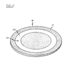
- Fig. 2 is a schematic perspective view of an aluminum target having a sputter track provided with an aluminum oxide inclusion
- Fig. 3 is a partial top perspective view of an aluminum sputter target provided with an aluminum oxide inclusion
- Fig. 4 is a view of Fig. 3 after sputtering of the sputter target
- Fig. 5 is a partial top perspective view of an aluminum microparticle on a silicon wafer
- Fig. 6 is a graph representing the variation in total particle density found on silicon wafers with sputtering power density and inclusion size
- Fig. 7 is a graph representing the particle size distributions found on silicon wafers after sputtering at 8, 16, 24, and 32 W/cm 2 power densities with a 2940 ⁇ m inclusion in the target sputter track;
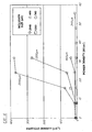
- Fig. 8 is a graph representing the variation in total particle defect density on the wafer after sputtering with embedded inclusion size for sputtering power densities of 8, 16, 24 and 32 W/CM 2 ;
- Fig. 9 is a graph representing the arc rate as a function of embedded Al 2 O 3 inclusion size at 8, 16, 24 and 32 W/cm 2 sputtering power densities;
- Fig. 10 is a graph representing the variation in inclusion critical size with sputtering power density for particle density and arc rate measurements
- Fig. 11 is a graph representing the correlation between arc rate and total particle defect density found on the wafer.
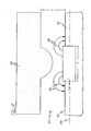
- Fig. 12 is a schematic diagram of the distortion of the plasma in a sputtering apparatus by inclusion charging caused by an Al 2 O 3 inclusion located on the surface of a sputter target.
- a sputter target assembly 10 preferably includes a backing plate 12 and a target 14 bonded together wherein the target 14 and backing plate 12 both are made of Al or Al alloys.
- the target 14 includes a sputtering surface 16 for sputtering in a sputtering apparatus (not shown) and preferably comprises a high grade Al or Al alloy.
- Preferred Al alloys for use in the target 14 and the backing plate 12 include Al-Cu alloys.
- An intermediate layer (not shown) may be provided between the target and backing plate.
- any conventionally available sputtering apparatus used for sputtering targets in a plasma preferably an argon plasma
- the plasmas in these conventional apparatuses form a plasma sheath having a known, or measurable, thickness under a selected sputtering environment. If the thickness of the sheath is unknown, it is preferably measured by providing a contaminant-free Al or Al alloy sputter target having an Al 2 O 3 inclusion-free sputtering surface for sputtering under a selected sputtering environment in the sputtering apparatus.
- the critical size of an Al 2 O 3 inclusion can be determined based upon the thickness of the sheath. More specifically, the diameter, or minimum effective diameter, of an Al 2 O 3 inclusion in an Al or Al alloy sputter target must be less than the thickness of the plasma sheath during sputtering under the selected sputtering environment to inhibit arcing. While some inclusions may be substantially circular in nature such that a diameter measurement easily can be realized, it is understood that a minimum effective diameter can be realized for Al 2 O 3 inclusions having somewhat irregular or non-circular shapes. Accordingly, diameter shall be used interchangeably with minimum effective diameter.
- the measured diameter is compared with the measured thickness of the plasma sheath. Additionally, since sputtering of the sputter target is performed at the sputtering surface, it is preferred that the measurement of the diameter of an Al 2 O 3 inclusion be taken along a plane substantially parallel with the sputtering surface.
- Al 2 O 3 inclusions that are located on the sputtering surface of an Al or Al alloy sputter target can be measured rather simplistically such as via scanning electron microscopy, or any other suitable measuring device or means.
- the inclusions provided within the sputter target, and not on the surface must be measured by other more involved methods such as via an ultrasonic scanning method like the one disclosed in U.S. Patent 5,406,850 . Additional measuring methods which may be suitable can be found in U.S. Provisional Patent Application Serial No. 09/700,268 filed November 9,2000 titled "Method and Apparatus for Quantitative Sputter Target Cleanliness and Characterization, U.S. Provisional Patent Application Serial No.
- a contaminate-free Al or Al alloy sputter target can be provided having no Al 2 O 3 inclusions with diameters greater than the measured thickness of the plasma sheath for sputtering in the sputtering apparatus under the selected sputtering environment.
- the sputter target can be sputtered in the sputtering apparatus under the selected sputtering environment, whereby arcing is inhibited.
- the softness of the aluminum and hardness of the Al 2 O 3 inclusions allowed the inclusions to remain mechanically locked in the sputtering surfaces of the aluminum targets.
- the inclusion particles were always placed in the centers of the magneton erosion or sputter tracks on the targets where sputtering occurred with more frequency.
- Fig. 2 shows a schematic diagram of the experimental arrangement where an aluminum target plate 18 has an embedded Al 2 O 3 inclusion 20 in the sputtering surface 21.
- Each Al target plate 18 was placed into a sputtering apparatus (not shown) and sputtered under a sputtering environment where the powers ranged from 8 W/cm 2 to 60 W/cm 2 at a 0.5 Pa argon pressure.
- the argon plasmas so generated were magnetically contained so that the targets operated in the DC magneton-sputtering mode.
- the 10 kW switching sputtering power supply used in this study was an Advanced Energy model 2012-061-m MDX-10K.
- Target/substrate spacing was 143 mm.
- Sputtering power density was calculated by dividing the sputtering power by the area of the sputtering track 23, which was 12.7 cm 2 for each target.
- Table 1 below provides the sputtering voltage, current, ion current density and the sheath thickness for the sputtering conditions used in this study.
- the ion current density was calculated by assuming a secondary electron coefficient of 0.045.
- the sheath thickness in the sputter track was calculated using the Child-Langmuir Law. From Table 1, the sheath thickness for the experimental conditions used in this study decreases from 600 ⁇ m at low power conditions to 300 ⁇ m at high power conditions. Sheath thickness for 24 W/cm 2 sputtering power was 440 ⁇ m.
- Figs 3 and 4 show an enlarged -3 mm size Al 2 O 3 inclusion 22 embedded into the sputtering surface 24 of an aluminum target plate 26 before and after sputtering.
- the inclusion 22 remains well attached to the sputtering surface 24 with little change in size or shape after sputtering.
- the sputtering process erodes the sputtering surface 24 so that some grain boundary structure 28 can be seen after sputtering as suggested in Fig. 4 .
- Polished 150 mm diameter silicon wafers were used as the substrates for these experiments.
- Deposited films were analyzed for particulate defects using a Tencor 6420 surface analyzer. Each wafer was analyzed after sputter coating for 1 minute. Particulate defects in the deposited film were grouped by apparent size with size bins ranging from 0.5 to 12 ⁇ m.
- the background particle density was measured by depositing aluminum films on wafers without an embedded inclusion. The background total particle density was 8.5 cm- 2 .
- the arc rate was measured by monitoring detected current pulses on the main power lead from the power supply to the sputtering cathode.
- a coil placed around the cathode power cable inductively detected the current pulses when arcs occurred.
- the voltage pulses induced in the sensing coil were recorded on an oscilloscope and a pulse counter.
- the arc rate was the total arc count divided by the deposition time.
- Fig. 5 shows aluminum macroparticles 30 captured on a silicon wafer 32 during aluminum sputter deposition.
- the relative large volume of the large macroparticle 34 and the flattened shape shown in Fig. 5 are often seen in large macroparticles.
- Macroparticles 30 emitted during the early stages of an arc or emitted as a result of surface contamination tend to be smaller and more spherical in shape.
- the shapes of the macroparticles 30 after solidification depend upon the surface tension of the liquid and the diameter of the macroparticle droplets prior to freezing on the wafer 32.
- R a and P d represent the arc rate and the measured density of particles found on the wafer. At low sputtering power density, no macroparticles were detected above the background level. Inclusions with diameters of less than 340 ⁇ m did not cause ejection of measurable macroparticles even at power densities of over 50 W/cm. As the diameters of the inclusions increased from 340 ⁇ m, the total particle densities found on the wafers increased.
- the sputtering power density required to generate particle defects on the wafers decreased to the point that for an inclusion having a diameter of 2940 ⁇ m, a significant increase in particle defect density on the wafer was found with a sputtering power density of only 16 W/cm 2 .
- the size distributions of the macroparticle defects on the wafers after sputtering with 2940 ⁇ m inclusions in the target surfaces is provided in Fig. 7 . From this data, as the sputtering power density increased, the number of particle defects on the wafer increased in all size categories. Also, the majority of the particle defects (>60%) were less than 1.1 ⁇ m in size. This type of macroparticle size distribution is consistent with measurements of macroparticle size distributions emitted by vacuum arc studies with clean metallic surfaces.
- Fig. 8 shows how the total particle densities on the wafers varied with embedded inclusion size as the sputtering power density increased from 8 to 32 W/cm2. Below about 500 ⁇ m inclusion size, the defect particle density could not be distinguished above the background particle density on the wafer.
- the critical inclusion size for generation of macroparticles on the wafer above the background level was determined for each power density by doing a least-squares fit of the data for inclusion sizes greater than 340 ⁇ m.
- the lines in Fig. 8 show the least-squares fits of the data for the various power densities. It is clear that the slopes of the particle density versus inclusion size lines increases with sputtering power. However, the x-intercepts do not change significantly with sputtering power. All x-axis intercepts appear to be near the 500- ⁇ m-inclusion size.
- the critical inclusion size for initiation of arcing and molten macroparticles ejection for each data set is graphed in Fig. 10 as a function of the sputtering power density.
- the error bars are derived from the error of estimate obtained from the least-squares-fits in Figs. 8 and 9 .
- the data in Fig 10 gives an average value for the critical inclusion size of 440 ⁇ 160 ⁇ m. It can also be seen in Fig. 10 that the crucial inclusion size is within experimental error independent of the sputtering power density.
- the critical size is 440 ⁇ 160 ⁇ m for the conditions used in this study wherein the plasma sheath thickness ranged from 300 to 600 ⁇ m.
- the total particle defect density detected on the silicon wafer was 3 cm -2 when the 450- ⁇ m inclusion was used increasing to 11 cm -2 for the 730 ⁇ m inclusion.
- the critical inclusion size appears to be related to the conditions for initiating the arc and not related to conditions to form molten metal on the target surface or to break the molten metal surface tension for ejection of molten macroparticles from the cathode surface. It has already been shown that the force exerted by an arc on the cathode surface is more than sufficient to overcome the surface tension and eject molten macroparticles. So, once an arc occurs macroparticle ejection is likely. This is confirmed by comparing our measurements of particle defect density on the wafer with arc rate. The arc rate and the total particle defect density are clearly related to each other.
- Figure 11 shows the relationship between total particle defect density found on the wafer, P d , and the arc rate, R a , during film deposition.
- P d total particle defect density found on the wafer
- R a the arc rate
- FIG. 12 shows a schematic representation of the plasma 36 when an Al 2 O 3 inclusion 38 is present on the cathode sputtering surface 40 of a target plate 42 such that the diameter (d) of the Al 2 O 3 inclusion 38 is greater than the thickness (s) of the plasma sheath 44 that is located over an area of the target plate 42 free from Al 2 O 3 inclusions.
- the plasma sheath 44 separates the positive column of the plasma 36 and the cathode sputtering surface 40.
- the inclusion 38 on the sputtering surface 40 of the target plate 42 leads to distortion of the plasma 36 and the sheath 44. Since sputtering of the target plate 42 is performed at the sputtering surface 40, it is preferred that the measurement of the diameter (d) of the Al 2 O 3 inclusion 38 be taken along a plane 45 substantially parallel with the sputtering surface 40.
- the charge on the inclusion 38 acts to almost neutralize the electric field in the original sheath region above the inclusion 38. This causes the plasma boundary to sag toward the inclusion 38 and the plasma sheath thickness over the inclusion 38 decreases as the plasma positive column diffuses into the volume over the charged inclusion 38. As the plasma column diffuses, inward and the field barrier separating the plasma 36 from the cathode shrinks, a plasma channel forms over the inclusion. This plasma channel grows primarily by radial diffusion of the plasma 36.
- the electric field distribution around the inclusion also will not be symmetrical. Since the electric field distortion will tend to mimic the inclusion asymmetry, the radial growth of the plasma channel will also be asymmetrical.
- the plasma channel grows, a point is reached where conditions permit breakdown and an arc strikes between a site on the cathode surface near the inclusion and the plasma channel.
- the energy stored in the power supply (not shown) and the connecting cable (not shown) is discharged as an arc. This arc, once formed, is free to move across the cathode surface 40 creating arc tracks and ejecting molten macroparticles.
- the arc spot with this model will tend to occur on the metallic cathode surface 40 near the inclusion 38. This is consistent with observations that the arc tracks do not intersect the inclusions 38, but are near the inclusion 38.
- the aspect ratio of the inclusion 38 will be an important variable.
- This model predicts that the arc rate will also be relatively insensitive to the area of the inclusion 38. For example, a very narrow inclusion with large area will arc at the same rate as an inclusion with an aspect ratio of 1 and dimension equal to the narrow dimension of the much larger area narrow inclusion.
- the arc rate will depend on location of the inclusion with respect to the local current density and sheath thickness. That is, if the sputtering surface 40 corresponds to an imaginary surface (not shown) within the sputtering apparatus, the arc rate and, thus, the local critical diameter, will depend on location along that imaginary surface. Since for typical fixed magnet planar magnetron sputtering systems the current density over the surface of the target is highly non-uniform, the sheath thickness will also be non-uniform depending upon the local current density. From the Child-Langmuir law the sheath thickness in, for example, the sputter track area of a typical sputtering condition with 50 mA/cm 2 current density will be 0.4 mm.
- the critical inclusion size for arcing in fixed magnet systems depends on the location of the inclusion 38 on the target surface 40.
- the critical inclusion size decreases in the sputter track areas (high power density and smaller sheath thickness) and increases in non-sputter track areas (low power density and larger sheath thickness).
- arcing can still result indicating that the thickness aspect of the inclusion does not appear to play a significant role in the process.
Landscapes
- Chemical & Material Sciences (AREA)
- Engineering & Computer Science (AREA)
- Chemical Kinetics & Catalysis (AREA)
- Materials Engineering (AREA)
- Mechanical Engineering (AREA)
- Metallurgy (AREA)
- Organic Chemistry (AREA)
- Physics & Mathematics (AREA)
- Plasma & Fusion (AREA)
- Analytical Chemistry (AREA)
- Physical Vapour Deposition (AREA)
- Investigating And Analyzing Materials By Characteristic Methods (AREA)
Abstract
Description
- The present invention relates generally to aluminum or aluminum alloy sputter targets having aluminum oxide (Al2O3) inclusions and, more particularly, to a method for determining a critical size of an Al2O3 inclusion in an aluminum or aluminum alloy sputter target to inhibit bipolar arcing during sputtering thereof.
- The presence of an Al2O3 inclusion in an Al or Al alloy sputter target can result in arcing when the target is sputtered in a sputtering apparatus. During sputtering, an electric field forms in the sputtering apparatus between the target and an anode. This electric field ionizes a gas, such as argon, within the sputtering apparatus so as to form a plasma. Typically, a plasma sheath, or dark space, separates a positive column of the plasma from the sputter target. This sheath has a certain thickness. Introduction of an Al2O3 inclusion on the surface of the target can distort the electric field so as to alter the shapes of the positive plasma column and the plasma sheath.
- Over time, electrical charges can build up in the vicinity of an Al2O3 inclusion. When the electrical charge imbalance becomes sufficiently strong, a high current density cathodic arc forms. The high current density cathodic arc heats a small section of the target surface, often sufficiently to melt the target material in that section. The arc pressure causes droplets of liquid metal to eject from the sputtering target surface at high velocity and strike an intended substrate, such as a silicon chip. The droplets, or macroparticles, solidify on the substrate creating large defects thereon. These macroparticles can range in size from less than 1 µm to greater than 50 µm in diameter and can reduce significantly device yields, for example, in integrated circuit manufacturing.
- Dielectric inclusions and surface layers have long been known to cause arcing in plasma discharges as well as in vacuum spark gaps. For example Pavate et al in Proceedings of SPIE - The International Society for Optical Engineering, Vol 3214 ISSN: 0277-786/97 show that the presence of undesirable metallurgical attributes such as alumina inclusions, porosity, oxygen content etc. are primary causes of unipolar arcing, and that such arcing can be greatly reduced by minimizing such defects. More recently, research on arcing in sputtering plasmas has shown that inclusion and surface oxide induced arcing causes molten metal macroparticle ejection from aluminum sputtering targets producing particle defects on the substrate. High-speed video analysis of arcing from heavily doped aluminum-aluminum oxide sputtering targets has shown that the molten metal macroparticles ejected therefrom can have speeds of over 500 m/sec and temperatures of 3000 K.
- It has been reported that dielectric inclusions between 0.10 and 10 µm cause arc initiation in a hydrogen plasma with 0.1 mA/cm2 discharge current; hydrogen pressures between 2.7 and 13 Pa; and a cathode bias between 100 and 500 volts. Also, arcing from aluminum targets sputtered in 1014 ions/cm3 argon, hydrogen and nitrogen plasmas with 1-µm diameter Al2O3 inclusions on the cathode surface has been reported. Finally, evidence for a critical size effect for arc initiation from inclusions in hydrogen tokomak plasmas has been reported but critical inclusion sizes were not measured.
- Notably, attempts have been made to reproduce the above results where inclusion sizes were measured. As a result, it was determined that the arcs were a result of surface contamination and not the size of the inclusions. Apparently, the small values for the critical size of the inclusion for arc initiation that initially were reported appeared to be due to surface contamination effects. As such, it is important to provide contaminant-free sputter targets when examining the effect of inclusion sizes on arc initiation.
- Consequently, there remains a need in the art for methods to inhibit bipolar arcing in Aℓ or Aℓ alloy sputter targets having Aℓ2O3 inclusions. Such methods are calculated to improve device yields and decrease scrap, thereby reducing manufacturing costs in fields such as the manufacture of integrated circuits.
- The present invention provides a method to inhibit arcing in an Aℓ or Aℓ alloy sputter target having an Aℓ2O3 inclusion comprising:
- (a) providing a sputtering apparatus having a plasma with a plasma sheath of a known thickness during sputtering, under a selected sputtering environment, of a first Aℓ or Aℓ alloy sputter target having an Aℓ2O3 inclusion-free sputtering surface;
- (b) providing a second Aℓ or Aℓ alloy sputter target having one or more Aℓ2O3 inclusions and a sputtering surface for sputtering in said sputtering apparatus under said selected sputtering environment wherein said one or more Aℓ2O3 inclusions include a diameter less than said known thickness of said plasma sheath; and
- (c) sputtering in said sputtering apparatus under said selected sputtering environment said second Aℓ or Aℓ alloy sputter target having said one or more Aℓ2O3 inclusions whereby arcing is inhibited.
- This method can be carried out using a sputtering apparatus having a plasma column, such as argon. The plasma has a plasma sheath of a known thickness during sputtering under a selected sputtering environment of an Aℓ or Aℓ alloy sputter target having an Aℓ2O3 inclusion-free sputtering surface for sputtering under a selected sputtering environment in the sputtering apparatus. The sheath thickness can then be calculated using the Child-Langmuir law by factoring in the known conditions for the selected sputtering environment including the sputtering voltage, ion mass and ion current density.
- When the thickness of the sheath is known, or measured, for a selected sputtering environment, the critical size of an Aℓ2O3 inclusion can be determined based upon the thickness of the sheath, More specifically, the diameter, or effective diameter, of an Aℓ2O3 inclusion in an Aℓ or Aℓ alloy sputter target must be less than the thickness of the plasma sheath during sputtering under the selected sputtering environment to inhibit arcing. Once the critical size is determined for the Aℓ2O3 inclusion, an Aℓ or Aℓ alloy sputter target having an Aℓ2O3 inclusion of a known diameter that is less than the thickness of the plasma sheath can be provided for sputtering in the sputtering apparatus under the selected sputtering environment so that bipolar arcing of the Aℓ or Aℓ alloy sputter target is inhibited. Since sputtering of the sputter target is performed at the sputtering surface, it is preferred that the measurement of the diameter of the Aℓ2O3 inclusion be taken in a plane substantially parallel with the sputtering surface.
- Being able to determine the critical size of an Aℓ2O3 inclusion in Aℓ or Aℓ alloy sputter target, will allow device yields, for example, in integrated circuit manufacturing, to increase and will allow scrapped products to be reduced resulting in a monetary savings for all involved.
- Accordingly, one object of the present invention is to determine the critical size for an Aℓ2O3 inclusion in an aluminum or aluminum alloy sputter target sputtered under plasma in a sputtering apparatus.
- Another object of the invention is to prevent arcing during sputtering of an Al or Al alloy sputter target having an Al2O3 inclusion.
- Yet, another object of the invention is to understand how the inclusion or surface oxide size affects the propensity of the sputtering plasma to arc, as well as to find the relationship between inclusion size, sputtering power, and the propensity for arcing and molten macroparticle ejection.
- Other objects and advantages of the invention will be apparent from the following description, the accompanying drawings and the appended claims.
-
Fig. 1 is a perspective view of a conventional sputter target assembly having a backing plate and a target; -
Fig. 2 is a schematic perspective view of an aluminum target having a sputter track provided with an aluminum oxide inclusion; -
Fig. 3 is a partial top perspective view of an aluminum sputter target provided with an aluminum oxide inclusion; -
Fig. 4 is a view ofFig. 3 after sputtering of the sputter target; -
Fig. 5 is a partial top perspective view of an aluminum microparticle on a silicon wafer; -
Fig. 6 is a graph representing the variation in total particle density found on silicon wafers with sputtering power density and inclusion size; -
Fig. 7 is a graph representing the particle size distributions found on silicon wafers after sputtering at 8, 16, 24, and 32 W/cm2 power densities with a 2940 µm inclusion in the target sputter track; -
Fig. 8 is a graph representing the variation in total particle defect density on the wafer after sputtering with embedded inclusion size for sputtering power densities of 8, 16, 24 and 32 W/CM2; -
Fig. 9 is a graph representing the arc rate as a function of embedded Al2O3 inclusion size at 8, 16, 24 and 32 W/cm2 sputtering power densities; -
Fig. 10 is a graph representing the variation in inclusion critical size with sputtering power density for particle density and arc rate measurements; -
Fig. 11 is a graph representing the correlation between arc rate and total particle defect density found on the wafer; and -
Fig. 12 is a schematic diagram of the distortion of the plasma in a sputtering apparatus by inclusion charging caused by an Al2O3 inclusion located on the surface of a sputter target. - We have discovered unexpectedly that there is a critical size for an Al2O3 inclusion for initiating arcing and molten macroparticle emission during sputtering of Al or Al alloy sputter targets in a plasma in a sputtering apparatus. As shown in
Fig. 1 , asputter target assembly 10 preferably includes abacking plate 12 and atarget 14 bonded together wherein thetarget 14 andbacking plate 12 both are made of Al or Al alloys. Thetarget 14 includes a sputteringsurface 16 for sputtering in a sputtering apparatus (not shown) and preferably comprises a high grade Al or Al alloy. Preferred Al alloys for use in thetarget 14 and thebacking plate 12 include Al-Cu alloys. An intermediate layer (not shown) may be provided between the target and backing plate. - Any conventionally available sputtering apparatus used for sputtering targets in a plasma, preferably an argon plasma, can be used. The plasmas in these conventional apparatuses form a plasma sheath having a known, or measurable, thickness under a selected sputtering environment. If the thickness of the sheath is unknown, it is preferably measured by providing a contaminant-free Al or Al alloy sputter target having an Al2O3 inclusion-free sputtering surface for sputtering under a selected sputtering environment in the sputtering apparatus. The sheath thickness can then be estimated using the Child-Langmuir law by factoring in the known conditions for the selected sputtering environment including the sputtering voltage, ion mass, and ion current density among others. More specifically, sheath thickness, s in MKS units becomes s = 4.7x10⁻¹¹ V3/4/(M¡-J¡)1/4 with V representing the sputtering voltage; Mi, the ion mass; and Ji, the ion current density.
- When the thickness of the sheath is known, or measured, for a selected sputtering environment, the critical size of an Al2O3 inclusion can be determined based upon the thickness of the sheath. More specifically, the diameter, or minimum effective diameter, of an Al2O3 inclusion in an Al or Al alloy sputter target must be less than the thickness of the plasma sheath during sputtering under the selected sputtering environment to inhibit arcing. While some inclusions may be substantially circular in nature such that a diameter measurement easily can be realized, it is understood that a minimum effective diameter can be realized for Al2O3 inclusions having somewhat irregular or non-circular shapes. Accordingly, diameter shall be used interchangeably with minimum effective diameter. It is this measured diameter that is compared with the measured thickness of the plasma sheath. Additionally, since sputtering of the sputter target is performed at the sputtering surface, it is preferred that the measurement of the diameter of an Al2O3inclusion be taken along a plane substantially parallel with the sputtering surface.
- Al2O3 inclusions that are located on the sputtering surface of an Al or Al alloy sputter target can be measured rather simplistically such as via scanning electron microscopy, or any other suitable measuring device or means. In contrast, the inclusions provided within the sputter target, and not on the surface, must be measured by other more involved methods such as via an ultrasonic scanning method like the one disclosed in
U.S. Patent 5,406,850 .
Additional measuring methods which may be suitable can be found inU.S. Provisional Patent Application Serial No. 09/700,268 filed November 9,2000 U.S. Provisional Patent Application Serial No. 60/197,790 filed April 14, 2000 U.S. Provisional Patent Application Serial No. 60/311,152 filed August 9, 2001 PCT/US01/14403 filed May 4, 2001 titled "Cleanliness Evaluation in Sputter Targets using Phase". - When an Al2O3 inclusion has a diameter less than the sheath thickness, arcing behavior is inhibited when the inclusion is exposed to the sputtering plasma. When the inclusion has a diameter that is substantially equal to or greater than the plasma sheath, then bipolar arcing will occur causing significant arcing activity during sputtering with ejection of molten metal macroparticles from the interaction of the charged dielectric inclusion surface with the sputtering plasma. As such, if the Al2O3 inclusions in the Al or Al alloy sputter target are too large in diameter, the target is rejected.
- Once the critical size is determined for the Al2O3 inclusion, a contaminate-free Al or Al alloy sputter target can be provided having no Al2O3 inclusions with diameters greater than the measured thickness of the plasma sheath for sputtering in the sputtering apparatus under the selected sputtering environment. Finally, the sputter target can be sputtered in the sputtering apparatus under the selected sputtering environment, whereby arcing is inhibited.
- The following example is provided for illustrative purposes only.
- To understand how the size of the Al2O3 inclusion in an Al or Al alloy sputter target affects the propensity for the plasma in a sputtering apparatus to breakdown into an arc during sputtering, the following sputtering experiments were conducted in a cryopumped vacuum chamber using a 7.6 cm diameter aluminum sputtering target. The thickness of the plasma sheath in this study was controlled and determined to be between 300 and 600 µm during sputtering of the aluminum target under a selected sputtering environment as discussed below.
- To begin, small holes were drilled into the face of sputtering targets and small (0.01 to 3 mm) Al2O3 inclusions were placed into the holes using tweezers. For purposes of the experiments herein, only Al2O3 inclusions having an aspect ratio of about 1 were tested.
- The softness of the aluminum and hardness of the Al2O3 inclusions allowed the inclusions to remain mechanically locked in the sputtering surfaces of the aluminum targets. The inclusion particles were always placed in the centers of the magneton erosion or sputter tracks on the targets where sputtering occurred with more frequency.
-
Fig. 2 shows a schematic diagram of the experimental arrangement where analuminum target plate 18 has an embedded Al2O3 inclusion 20 in the sputteringsurface 21. EachAl target plate 18 was placed into a sputtering apparatus (not shown) and sputtered under a sputtering environment where the powers ranged from 8 W/cm2 to 60 W/cm2 at a 0.5 Pa argon pressure. The argon plasmas so generated were magnetically contained so that the targets operated in the DC magneton-sputtering mode. The 10 kW switching sputtering power supply used in this study was an Advanced Energy model 2012-061-m MDX-10K. Target/substrate spacing was 143 mm. Sputtering power density was calculated by dividing the sputtering power by the area of the sputteringtrack 23, which was 12.7 cm2 for each target. - Table 1 below provides the sputtering voltage, current, ion current density and the sheath thickness for the sputtering conditions used in this study.
Power Density V I Ji s (W/cm2) (Volts) (Amps) (A/m2) (mm) 8 405 0.26 194 0.60 16 459 0.46 344 0.49 24 486 0.64 479 0.44 32 496 0.82 613 0.39 40 505 1.00 748 0.36 48 518 1.16 868 0.34 56 503 1.40 1047 0.30 - The ion current density was calculated by assuming a secondary electron coefficient of 0.045. The sheath thickness in the sputter track was calculated using the Child-Langmuir Law. From Table 1, the sheath thickness for the experimental conditions used in this study decreases from 600 µm at low power conditions to 300 µm at high power conditions. Sheath thickness for 24 W/cm2 sputtering power was 440 µm.
-
Figs 3 and 4 show an enlarged -3 mm size Al2O3 inclusion 22 embedded into the sputteringsurface 24 of an aluminum target plate 26 before and after sputtering. As shown inFig. 4 , theinclusion 22 remains well attached to the sputteringsurface 24 with little change in size or shape after sputtering. The sputtering process erodes the sputteringsurface 24 so that somegrain boundary structure 28 can be seen after sputtering as suggested inFig. 4 . - Polished 150 mm diameter silicon wafers were used as the substrates for these experiments. Deposited films were analyzed for particulate defects using a Tencor 6420 surface analyzer. Each wafer was analyzed after sputter coating for 1 minute. Particulate defects in the deposited film were grouped by apparent size with size bins ranging from 0.5 to 12 µm. The background particle density was measured by depositing aluminum films on wafers without an embedded inclusion. The background total particle density was 8.5 cm-2.
- The arc rate was measured by monitoring detected current pulses on the main power lead from the power supply to the sputtering cathode. A coil placed around the cathode power cable inductively detected the current pulses when arcs occurred. The voltage pulses induced in the sensing coil were recorded on an oscilloscope and a pulse counter. The arc rate was the total arc count divided by the deposition time.
- Molten macroparticle ejection during arcing of sputtering targets produces defects that have a particular morphology arising from their molten origin.
Fig. 5 showsaluminum macroparticles 30 captured on asilicon wafer 32 during aluminum sputter deposition. The relative large volume of thelarge macroparticle 34 and the flattened shape shown inFig. 5 are often seen in large macroparticles.Macroparticles 30 emitted during the early stages of an arc or emitted as a result of surface contamination tend to be smaller and more spherical in shape. The shapes of themacroparticles 30 after solidification depend upon the surface tension of the liquid and the diameter of the macroparticle droplets prior to freezing on thewafer 32. - Measurements of the total macroparticle densities found on the wafers after sputtering for 1 minute with various size inclusions embedded into the faces of the target erosion tracks at various sputtering powers are provided in Table 2 below and graphically in
Fig. 6 .Inclusion Size (µm) Power 130 340 450 460 1200 2940 Density Ra Pd Ra Pd Ra Pd Ra Pd Ra Pd Ra Pd (W/cm2) (sec-1) (cm-1) (sec-1) (cm-12) (scc-1) (cm-2) (sec-1) (cm-2) (sec-1) (cm-2) (sec-1) (cm-2) 8 0 3.9 0 0 7.0 0 2.5 0 6.6 5 17 16 0 2.7 0 0.2 3.8 0.9 3.4 0.6 38 433 72 24 0 3.0 0 3.4 3.1 99 16 356 59 10718 368 32 1.6 0 1.4 81 19 914 39 2456 269 8934 377 40 0 2.2 48 0 3.5 56 0 12 - In Table 2 above, Ra and Pd represent the arc rate and the measured density of particles found on the wafer. At low sputtering power density, no macroparticles were detected above the background level. Inclusions with diameters of less than 340 µm did not cause ejection of measurable macroparticles even at power densities of over 50 W/cm. As the diameters of the inclusions increased from 340 µm, the total particle densities found on the wafers increased. Also, the sputtering power density required to generate particle defects on the wafers decreased to the point that for an inclusion having a diameter of 2940 µm, a significant increase in particle defect density on the wafer was found with a sputtering power density of only 16 W/cm2.
- So from this data, it can be concluded that there are two factors controlling the emission of macroparticles from a sputtering target: the sputtering plasma conditions and the size of dielectric inclusions. When the diameters of the dielectric inclusion falls below a critical value, arcing and macroparticle emission do not occur.
- The size distributions of the macroparticle defects on the wafers after sputtering with 2940 µm inclusions in the target surfaces is provided in
Fig. 7 . From this data, as the sputtering power density increased, the number of particle defects on the wafer increased in all size categories. Also, the majority of the particle defects (>60%) were less than 1.1 µm in size. This type of macroparticle size distribution is consistent with measurements of macroparticle size distributions emitted by vacuum arc studies with clean metallic surfaces. During the arc, most of the particles emitted are small, fast-moving particles emitted at an angle of 30° from the plane of the cathode, but a small number of very large slow moving particles are emitted with trajectories near perpendicular to the cathode surface. These are the types of particles shown inFig. 5 and represented inFig. 7 in the large size end of the size distribution. -
Fig. 8 shows how the total particle densities on the wafers varied with embedded inclusion size as the sputtering power density increased from 8 to 32 W/cm2. Below about 500 µm inclusion size, the defect particle density could not be distinguished above the background particle density on the wafer. The critical inclusion size for generation of macroparticles on the wafer above the background level was determined for each power density by doing a least-squares fit of the data for inclusion sizes greater than 340 µm. The lines inFig. 8 show the least-squares fits of the data for the various power densities. It is clear that the slopes of the particle density versus inclusion size lines increases with sputtering power. However, the x-intercepts do not change significantly with sputtering power. All x-axis intercepts appear to be near the 500-µm-inclusion size. - A similar result is obtained if we plot the arc rate as a function of inclusion size. This data is shown in
Fig. 9 . Again, as the power density increases the slope of the arc rate versus inclusion size curves increase while the x-intercept remains relatively constant. In the case of the curves at 24 and 32 W/cm2, the slopes of both curves are equal within experimental error. This suggests that the arc rate may be reaching a saturation condition at 24 W/cm2 so that increasing sputtering power density does not generate an increase in arc rate at these high power densities. - The critical inclusion size for initiation of arcing and molten macroparticles ejection for each data set is graphed in
Fig. 10 as a function of the sputtering power density. The error bars are derived from the error of estimate obtained from the least-squares-fits inFigs. 8 and9 . The data inFig 10 gives an average value for the critical inclusion size of 440 ± 160µm. It can also be seen inFig. 10 that the crucial inclusion size is within experimental error independent of the sputtering power density. The critical size is 440 ± 160 µm for the conditions used in this study wherein the plasma sheath thickness ranged from 300 to 600 µm. - These single inclusion experiments were repeated using a commercial sputtering source used for aluminum alloy deposition on 200-mm diameter silicon wafers. This sputtering source used a rotating magnet for plasma confinement and improved film uniformity and target utilization. Inclusions with sizes of 450 and 730 µm were embedded into the aluminum sputtering target surface and the target was sputtered at 10.6 kW power with 0.5 Pa argon pressure. Measurements of the arc rate and particle defect density on 200 mm silicon wafers after sputtering for 1 minute showed results consistent with the data reported herein for the 7.6 cm diameter target. The arc rate was 2.5 sec-1 with the 450-µm inclusion increasing to 52 sec-1. when the 730-µm inclusion was embedded. Similarly, the total particle defect density detected on the silicon wafer was 3 cm-2 when the 450-µm inclusion was used increasing to 11 cm-2 for the 730 µm inclusion. These values fit the data in
Figs. 9 and10 for power density of 24 W/cm2. - In light of the above, the critical inclusion size appears to be related to the conditions for initiating the arc and not related to conditions to form molten metal on the target surface or to break the molten metal surface tension for ejection of molten macroparticles from the cathode surface. It has already been shown that the force exerted by an arc on the cathode surface is more than sufficient to overcome the surface tension and eject molten macroparticles. So, once an arc occurs macroparticle ejection is likely. This is confirmed by comparing our measurements of particle defect density on the wafer with arc rate. The arc rate and the total particle defect density are clearly related to each other.
Figure 11 shows the relationship between total particle defect density found on the wafer, Pd, and the arc rate, Ra, during film deposition. For the target-substrate geometry used in this study, at arc rates below about 2500 sec-1 one particle is detected on the wafer for every ten arc events. - Without wishing to be bound to any theory of operation, arc formation and ejection of the molten metal macroparticles appears to be based upon the interaction of the dielectric surface of the inclusion with the sputtering plasma.
Figure 12 shows a schematic representation of theplasma 36 when an Al2O3 inclusion 38 is present on thecathode sputtering surface 40 of atarget plate 42 such that the diameter (d) of the Al2O3inclusion 38 is greater than the thickness (s) of the plasma sheath 44 that is located over an area of thetarget plate 42 free from Al2O3 inclusions. Notably, the plasma sheath 44 separates the positive column of theplasma 36 and thecathode sputtering surface 40. Introduction of the inclusion 38 on the sputteringsurface 40 of thetarget plate 42 leads to distortion of theplasma 36 and the sheath 44. Since sputtering of thetarget plate 42 is performed at the sputteringsurface 40, it is preferred that the measurement of the diameter (d) of the Al2O3 inclusion 38 be taken along aplane 45 substantially parallel with the sputteringsurface 40. - Detailed examination of the process that leads to sheath disruption and the formation of the arc, as represented by
arrows 46 inFig. 12 , begins with the charging of the dielectric surface layer from ion bombardment during the sputtering process. This charge distorts the electric field in the dark space about the dielectric region. The severity of this electric field distortion depends on the relationship between diameter (d) of the dielectric inclusion and the sheath thickness (s). For small diameter inclusions, when the inclusion exposed to the plasma is significantly less than the sheath thickness, the disruption to the electric field in the dark space is concentrated in the vicinity of the inclusion. In fact, when the dielectric inclusion size exposed to the plasma is much less than the plasma sheath thickness (s0, the disturbance of the plasma sheath above and away from the inclusion surface is negligible. - As the inclusion 38 exposed to the
plasma 36 approaches a diameter (d) that is equal to or greater than the sheath thickness (s), the charge on the inclusion 38 acts to almost neutralize the electric field in the original sheath region above the inclusion 38. This causes the plasma boundary to sag toward the inclusion 38 and the plasma sheath thickness over the inclusion 38 decreases as the plasma positive column diffuses into the volume over the charged inclusion 38. As the plasma column diffuses, inward and the field barrier separating theplasma 36 from the cathode shrinks, a plasma channel forms over the inclusion. This plasma channel grows primarily by radial diffusion of theplasma 36. - Since one cannot expect the inclusion to be perfectly symmetrical, the electric field distribution around the inclusion also will not be symmetrical. Since the electric field distortion will tend to mimic the inclusion asymmetry, the radial growth of the plasma channel will also be asymmetrical. As the plasma channel grows, a point is reached where conditions permit breakdown and an arc strikes between a site on the cathode surface near the inclusion and the plasma channel. When the arc occurs, the energy stored in the power supply (not shown) and the connecting cable (not shown) is discharged as an arc. This arc, once formed, is free to move across the
cathode surface 40 creating arc tracks and ejecting molten macroparticles. - As described above, the arc spot with this model will tend to occur on the
metallic cathode surface 40 near the inclusion 38. This is consistent with observations that the arc tracks do not intersect the inclusions 38, but are near the inclusion 38. - If this model is correct, then we would expect that when the aspect ratio of the inclusion 38 deviates from one, the smaller dimension of the inclusion 38 will control the field distribution distortion over the inclusion 38 and therefore will control the degree of sheath distortion and the propensity for arcing. So, from our model, the aspect ratio of the inclusion 38 will be an important variable. This model predicts that the arc rate will also be relatively insensitive to the area of the inclusion 38. For example, a very narrow inclusion with large area will arc at the same rate as an inclusion with an aspect ratio of 1 and dimension equal to the narrow dimension of the much larger area narrow inclusion.
- Also, the arc rate will depend on location of the inclusion with respect to the local current density and sheath thickness. That is, if the sputtering
surface 40 corresponds to an imaginary surface (not shown) within the sputtering apparatus, the arc rate and, thus, the local critical diameter, will depend on location along that imaginary surface. Since for typical fixed magnet planar magnetron sputtering systems the current density over the surface of the target is highly non-uniform, the sheath thickness will also be non-uniform depending upon the local current density. From the Child-Langmuir law the sheath thickness in, for example, the sputter track area of a typical sputtering condition with 50 mA/cm2 current density will be 0.4 mm. However, moving away from the sputter track to the areas where current densities decrease to 10 mA/cm2 will increase the sheath thickness to 0.9 mm. Therefore, the critical inclusion size for arcing in fixed magnet systems depends on the location of the inclusion 38 on thetarget surface 40. The critical inclusion size decreases in the sputter track areas (high power density and smaller sheath thickness) and increases in non-sputter track areas (low power density and larger sheath thickness). Lastly, when a thin inclusion is present on the sputtering target surface, arcing can still result indicating that the thickness aspect of the inclusion does not appear to play a significant role in the process. - While the methods herein described constitute preferred embodiments of this invention, it is to be understood that the invention is not limited to these precise methods and that changes may be made without departing from the scope of the invention, which is defined in the appended claims.
Claims (11)
- A method to inhibit arcing in an Aℓ or Aℓ alloy sputter target having an Aℓ2O3 inclusion comprising:(a) providing a sputtering apparatus having a plasma with a plasma sheath of a known thickness during sputtering, under a selected sputtering environment, of a first Aℓ or Aℓ alloy sputter target having an Al2O3 inclusion-free sputtering surface;(b) providing a second Aℓ or Aℓ alloy sputter target having one or more Al2O3 inclusions and a sputtering surface for sputtering in said sputtering apparatus under said selected sputtering environment wherein said one or more Al2O3 inclusions include a diameter less than said known thickness of said plasma sheath; and(c) sputtering in said sputtering apparatus under said selected sputtering environment said second Aℓ or Aℓ alloy sputter target having said one or more Al2O3 inclusions whereby arcing is inhibited.
- A method according to claim 1 wherein said plasma is argon.
- A method according to claim 1 wherein said diameter of said one or more Al2O3 inclusions is situated in a plane substantially parallel with said sputtering surface of said second Aℓ or Aℓ alloy sputter target.
- A method according to claim 1 wherein said one or more Al2O3 inclusions have an aspect ratio of about 1.
- A method according to claim 1 wherein said first and second Aℓ or Aℓ alloy sputter targets are free from surface contamination.
- A method according to claim 1 wherein said known thickness of said plasma sheath is between 300 and 600 µm.
- A method according to claim 6 wherein said sputtering environment includes a 0.5 Pa argon pressure and a sputtering power from 8 W/cm2 to 60 W/cm2
- A method according to claim 1 wherein said second Aℓ or Aℓ alloy sputter target is similar in shape and size to said first Aℓ or Aℓ alloy sputter target having said Aℓ2O3 inclusion-free sputtering surface.
- A method according to claim 1 wherein said sputtering apparatus is capable of sputtering in an argon atmosphere at a sputtering power of between 8 W/cm2 and 60 W/cm2.
- A method according to claim 1 where in said step (a) includes sputtering said first Aℓ or Aℓ alloy sputtering target substantially free of Al2O3 inclusions in said sputtering apparatus in a gas defining an ion mass at a sputtering voltage; determining said ion mass; determining said sputtering voltage; determining an ion current density at a surface of said first Aℓ or Aℓ alloy sputtering target; and estimating said plasma sheath thickness using said ion mass, said sputtering voltage, and said ion current density.
- A method according to claim 1 wherein said step (a) includes sputtering said first Aℓ or Aℓ alloy sputter target substantially free of Aℓ2O3 inclusions in said sputtering apparatus in a gas defining an ion mass Mi at a sputtering voltage V; determining said ion mass Mi; determining said sputtering voltage V; determining an ion currency density Ji at a surface of said Aℓ or Aℓ alloy sputtering target; and estimating said plasma sheath thickness s using the equation s = 4.7 x 10⁻¹¹V¾ / (Mi .J¡)¼.
Applications Claiming Priority (3)
| Application Number | Priority Date | Filing Date | Title |
|---|---|---|---|
| US28148201P | 2001-04-04 | 2001-04-04 | |
| US281482P | 2001-04-04 | ||
| PCT/US2002/010516 WO2002081767A2 (en) | 2001-04-04 | 2002-04-04 | A method for determining a critical size of an inclusion in aluminum or aluminum alloy sputtering target |
Publications (3)
| Publication Number | Publication Date |
|---|---|
| EP1381703A2 EP1381703A2 (en) | 2004-01-21 |
| EP1381703A4 EP1381703A4 (en) | 2008-04-09 |
| EP1381703B1 true EP1381703B1 (en) | 2011-01-26 |
Family
ID=23077487
Family Applications (1)
| Application Number | Title | Priority Date | Filing Date |
|---|---|---|---|
| EP02719429A Expired - Lifetime EP1381703B1 (en) | 2001-04-04 | 2002-04-04 | A method for determining a critical size of an inclusion in aluminum or aluminum alloy sputtering target |
Country Status (6)
| Country | Link |
|---|---|
| US (1) | US7087142B2 (en) |
| EP (1) | EP1381703B1 (en) |
| JP (1) | JP4303970B2 (en) |
| KR (1) | KR100841915B1 (en) |
| DE (1) | DE60239054D1 (en) |
| WO (1) | WO2002081767A2 (en) |
Families Citing this family (3)
| Publication number | Priority date | Publication date | Assignee | Title |
|---|---|---|---|---|
| JP4349904B2 (en) | 2001-08-09 | 2009-10-21 | トーソー エスエムディー,インク. | Method and apparatus for non-destructive target cleanliness characterization by defect type categorized by size and location |
| TWI247576B (en) * | 2003-03-28 | 2006-01-11 | Hon Hai Prec Ind Co Ltd | Method of manufacturing electromagnetic interference shield |
| US10201070B2 (en) * | 2012-01-10 | 2019-02-05 | Electron Power Systems, Inc. | Systems and methods for generating electron spiral toroids |
Family Cites Families (39)
| Publication number | Priority date | Publication date | Assignee | Title |
|---|---|---|---|---|
| NL104695C (en) * | 1955-06-20 | |||
| US4054173A (en) * | 1974-12-23 | 1977-10-18 | Hunter Engineering Co., Inc. | Apparatus for producing completely recrystallized metal sheet |
| US4474225A (en) * | 1982-05-24 | 1984-10-02 | Aluminum Company Of America | Method of direct chill casting |
| US4568007A (en) * | 1984-01-23 | 1986-02-04 | Vesuvius Crucible Company | Refractory shroud for continuous casting |
| US4933296A (en) | 1985-08-02 | 1990-06-12 | General Electric Company | N+ amorphous silicon thin film transistors for matrix addressed liquid crystal displays |
| US4740481A (en) * | 1986-01-21 | 1988-04-26 | Motorola Inc. | Method of preventing hillock formation in polysilicon layer by oxygen implanation |
| US5177035A (en) * | 1986-06-27 | 1993-01-05 | The Carborundum Company | Molten metal filter and method for making same |
| US4797164A (en) * | 1986-09-30 | 1989-01-10 | Swiss Aluminum Ltd. | Process for manufacturing a fine-grained recrystallized sheet |
| DE69027158T2 (en) | 1989-08-11 | 1996-10-24 | Sharp Kk | Light addressed liquid crystal display device |
| US5191452A (en) | 1989-09-20 | 1993-03-02 | Honeywell Inc. | Active matrix liquid crystal display fabrication for grayscale |
| FR2664618B1 (en) * | 1990-07-10 | 1993-10-08 | Pechiney Aluminium | PROCESS FOR THE MANUFACTURE OF CATHODES FOR CATHODE SPRAYING BASED ON VERY HIGH PURITY ALUMINUM. |
| JP2610698B2 (en) | 1990-07-17 | 1997-05-14 | シャープ株式会社 | Method for manufacturing reflective liquid crystal display device |
| CA2084247A1 (en) | 1992-03-18 | 1993-09-19 | Francis Paul Fehlner | Lcd panel production |
| US6022458A (en) * | 1992-12-07 | 2000-02-08 | Canon Kabushiki Kaisha | Method of production of a semiconductor substrate |
| US5406850A (en) * | 1993-01-14 | 1995-04-18 | Tosoh Smd, Inc. | Method of non-destructively testing a sputtering target |
| US5738767A (en) * | 1994-01-11 | 1998-04-14 | Intevac, Inc. | Substrate handling and processing system for flat panel displays |
| KR100327716B1 (en) | 1994-01-11 | 2002-06-27 | 노만 에이취. 폰드 | Substrate operating method in vacuum processing system and vacuum processing system |
| CN1269196C (en) * | 1994-06-15 | 2006-08-09 | 精工爱普生株式会社 | Method for making thin-film semiconductor device |
| US5651865A (en) * | 1994-06-17 | 1997-07-29 | Eni | Preferential sputtering of insulators from conductive targets |
| CA2128398C (en) * | 1994-07-19 | 2007-02-06 | John Sulzer | Process and apparatus for casting metal strip and injector used therefor |
| US5559614A (en) * | 1995-05-01 | 1996-09-24 | Motorola, Inc. | Liquid crystal display with integral heater and method of fabricating same |
| JP3390579B2 (en) * | 1995-07-03 | 2003-03-24 | アネルバ株式会社 | Method and apparatus for producing thin film for liquid crystal display |
| US5804730A (en) * | 1995-10-10 | 1998-09-08 | Pfannenstiel; Richard A. | Ultrasonic testing method |
| FR2744805B1 (en) | 1996-02-13 | 1998-03-20 | Pechiney Aluminium | CATHODE SPRAY TARGETS SELECTED BY ULTRASONIC CONTROL FOR THEIR LOW PARTICLE EMISSION RATES |
| JPH09258247A (en) * | 1996-03-26 | 1997-10-03 | Sharp Corp | Liquid crystal display manufacturing method and film forming apparatus |
| US5943559A (en) * | 1997-06-23 | 1999-08-24 | Nec Corporation | Method for manufacturing liquid crystal display apparatus with drain/source silicide electrodes made by sputtering process |
| US5894188A (en) * | 1997-09-17 | 1999-04-13 | Candescent Technologies Corporation | Dual-layer metal for flat panel display |
| US6001227A (en) * | 1997-11-26 | 1999-12-14 | Applied Materials, Inc. | Target for use in magnetron sputtering of aluminum for forming metallization films having low defect densities and methods for manufacturing and using such target |
| US6139701A (en) * | 1997-11-26 | 2000-10-31 | Applied Materials, Inc. | Copper target for sputter deposition |
| US6020946A (en) * | 1998-02-23 | 2000-02-01 | International Business Machines Corporation | Dry processing for liquid-crystal displays using low energy ion bombardment |
| JP4436970B2 (en) | 1998-06-09 | 2010-03-24 | トーソー エスエムディー,インク. | Method and apparatus for quantitative determination of sputter target cleanliness characteristics |
| KR100642034B1 (en) | 1998-09-11 | 2006-11-03 | 토소우 에스엠디, 인크 | Low temperature sputter target bonding method and target assembly manufactured by this method |
| US6074455A (en) * | 1999-01-27 | 2000-06-13 | Metaullics Systems Co., L.P. | Aluminum scrap melting process and apparatus |
| US6269699B1 (en) * | 1999-11-01 | 2001-08-07 | Praxair S. T. Technology, Inc. | Determination of actual defect size in cathode sputter targets subjected to ultrasonic inspection |
| US20020184970A1 (en) * | 2001-12-13 | 2002-12-12 | Wickersham Charles E. | Sptutter targets and methods of manufacturing same to reduce particulate emission during sputtering |
| JP5368663B2 (en) | 2000-04-14 | 2013-12-18 | トーソー エスエムディー,インク. | Sputter target for reducing particulate emission during spattering and method for manufacturing the same |
| WO2001086282A1 (en) | 2000-05-11 | 2001-11-15 | Tosoh Smd, Inc. | Cleanliness evaluation in sputter targets using phase |
| US6439054B1 (en) * | 2000-05-31 | 2002-08-27 | Honeywell International Inc. | Methods of testing sputtering target materials |
| JP4349904B2 (en) | 2001-08-09 | 2009-10-21 | トーソー エスエムディー,インク. | Method and apparatus for non-destructive target cleanliness characterization by defect type categorized by size and location |
-
2002
- 2002-04-04 JP JP2002579526A patent/JP4303970B2/en not_active Expired - Fee Related
- 2002-04-04 US US10/473,844 patent/US7087142B2/en not_active Expired - Lifetime
- 2002-04-04 WO PCT/US2002/010516 patent/WO2002081767A2/en not_active Ceased
- 2002-04-04 KR KR1020037013047A patent/KR100841915B1/en not_active Expired - Fee Related
- 2002-04-04 EP EP02719429A patent/EP1381703B1/en not_active Expired - Lifetime
- 2002-04-04 DE DE60239054T patent/DE60239054D1/en not_active Expired - Lifetime
Also Published As
| Publication number | Publication date |
|---|---|
| KR100841915B1 (en) | 2008-06-30 |
| WO2002081767A3 (en) | 2002-12-05 |
| EP1381703A4 (en) | 2008-04-09 |
| US7087142B2 (en) | 2006-08-08 |
| WO2002081767A2 (en) | 2002-10-17 |
| DE60239054D1 (en) | 2011-03-10 |
| JP4303970B2 (en) | 2009-07-29 |
| KR20040011495A (en) | 2004-02-05 |
| US20040118675A1 (en) | 2004-06-24 |
| EP1381703A2 (en) | 2004-01-21 |
| JP2004526865A (en) | 2004-09-02 |
Similar Documents
| Publication | Publication Date | Title |
|---|---|---|
| US5202008A (en) | Method for preparing a shield to reduce particles in a physical vapor deposition chamber | |
| EP0561641B1 (en) | Method of sputtering a carbon protective film on a magnetic disk by superimposing an AC voltage on a DC bias voltage | |
| US6620296B2 (en) | Target sidewall design to reduce particle generation during magnetron sputtering | |
| US6171455B1 (en) | Target for use in magnetron sputtering of aluminum for forming metallization films having low defect densities and methods for manufacturing and using such target | |
| US5584972A (en) | Plasma noise and arcing suppressor apparatus and method for sputter deposition | |
| Koski et al. | Surface defects and arc generation in reactive magnetron sputtering of aluminium oxide thin films | |
| WO2000008228A1 (en) | Dual collimator physical-vapor deposition apparatus | |
| EP0446657B1 (en) | Method for preparing a shield to reduce particles in a physical vapor deposition chamber | |
| US7115193B2 (en) | Sputtering target producing very few particles, backing plate or apparatus within sputtering device and roughening method by electric discharge machining | |
| US6117281A (en) | Magnetron sputtering target for reduced contamination | |
| Löwe et al. | Control of ion energy and flux in a dual radio frequency excitation magnetron sputtering discharge | |
| JPH0762531A (en) | Method of depositing film on substrate by sputtering method | |
| US7087142B2 (en) | Method for determining a critical size of an inclusion in aluminum or aluminum alloy sputtering target | |
| Wickersham Jr et al. | Measurements of the critical inclusion size for arcing and macroparticle ejection from aluminum sputtering targets | |
| Carter et al. | Parameter optimization in pulsed DC reactive sputter deposition of aluminum oxide | |
| JP6539649B2 (en) | Target for reactive sputter deposition of electrically insulating layers | |
| US6090246A (en) | Methods and apparatus for detecting reflected neutrals in a sputtering process | |
| WO2001094659A2 (en) | Sputtering target | |
| JPH11152564A (en) | Presputtering method and device | |
| JP2000144417A (en) | High frequency sputtering equipment | |
| CN115595544B (en) | Method for detecting sputtering performance of metal target | |
| JPH0867981A (en) | Sputtering device | |
| Takagi et al. | Suppression of high-energy backscattered particles in magnetron plasma using cylindrical cathode | |
| JPS5887271A (en) | Planar magnetron sputtering equipment | |
| JP2003105536A (en) | Sputtering equipment |
Legal Events
| Date | Code | Title | Description |
|---|---|---|---|
| PUAI | Public reference made under article 153(3) epc to a published international application that has entered the european phase |
Free format text: ORIGINAL CODE: 0009012 |
|
| 17P | Request for examination filed |
Effective date: 20030926 |
|
| AK | Designated contracting states |
Kind code of ref document: A2 Designated state(s): AT BE CH CY DE DK ES FI FR GB GR IE IT LI LU MC NL PT SE TR |
|
| A4 | Supplementary search report drawn up and despatched |
Effective date: 20080306 |
|
| 17Q | First examination report despatched |
Effective date: 20100322 |
|
| GRAP | Despatch of communication of intention to grant a patent |
Free format text: ORIGINAL CODE: EPIDOSNIGR1 |
|
| GRAS | Grant fee paid |
Free format text: ORIGINAL CODE: EPIDOSNIGR3 |
|
| GRAA | (expected) grant |
Free format text: ORIGINAL CODE: 0009210 |
|
| AK | Designated contracting states |
Kind code of ref document: B1 Designated state(s): DE FR GB |
|
| REG | Reference to a national code |
Ref country code: GB Ref legal event code: FG4D |
|
| REF | Corresponds to: |
Ref document number: 60239054 Country of ref document: DE Date of ref document: 20110310 Kind code of ref document: P |
|
| REG | Reference to a national code |
Ref country code: DE Ref legal event code: R096 Ref document number: 60239054 Country of ref document: DE Effective date: 20110310 |
|
| PLBE | No opposition filed within time limit |
Free format text: ORIGINAL CODE: 0009261 |
|
| STAA | Information on the status of an ep patent application or granted ep patent |
Free format text: STATUS: NO OPPOSITION FILED WITHIN TIME LIMIT |
|
| 26N | No opposition filed |
Effective date: 20111027 |
|
| REG | Reference to a national code |
Ref country code: DE Ref legal event code: R097 Ref document number: 60239054 Country of ref document: DE Effective date: 20111027 |
|
| PGFP | Annual fee paid to national office [announced via postgrant information from national office to epo] |
Ref country code: GB Payment date: 20130429 Year of fee payment: 12 |
|
| PGFP | Annual fee paid to national office [announced via postgrant information from national office to epo] |
Ref country code: DE Payment date: 20140429 Year of fee payment: 13 |
|
| GBPC | Gb: european patent ceased through non-payment of renewal fee |
Effective date: 20140404 |
|
| PG25 | Lapsed in a contracting state [announced via postgrant information from national office to epo] |
Ref country code: GB Free format text: LAPSE BECAUSE OF NON-PAYMENT OF DUE FEES Effective date: 20140404 |
|
| REG | Reference to a national code |
Ref country code: DE Ref legal event code: R119 Ref document number: 60239054 Country of ref document: DE |
|
| PG25 | Lapsed in a contracting state [announced via postgrant information from national office to epo] |
Ref country code: DE Free format text: LAPSE BECAUSE OF NON-PAYMENT OF DUE FEES Effective date: 20151103 |
|
| REG | Reference to a national code |
Ref country code: FR Ref legal event code: PLFP Year of fee payment: 15 |
|
| REG | Reference to a national code |
Ref country code: FR Ref legal event code: PLFP Year of fee payment: 16 |
|
| PGFP | Annual fee paid to national office [announced via postgrant information from national office to epo] |
Ref country code: FR Payment date: 20170426 Year of fee payment: 16 |
|
| PG25 | Lapsed in a contracting state [announced via postgrant information from national office to epo] |
Ref country code: FR Free format text: LAPSE BECAUSE OF NON-PAYMENT OF DUE FEES Effective date: 20180430 |