EP1381137A2 - Voltage control circuit for a bicycle dynamo - Google Patents
Voltage control circuit for a bicycle dynamo Download PDFInfo
- Publication number
- EP1381137A2 EP1381137A2 EP03015492A EP03015492A EP1381137A2 EP 1381137 A2 EP1381137 A2 EP 1381137A2 EP 03015492 A EP03015492 A EP 03015492A EP 03015492 A EP03015492 A EP 03015492A EP 1381137 A2 EP1381137 A2 EP 1381137A2
- Authority
- EP
- European Patent Office
- Prior art keywords
- dynamo
- load
- sensor circuit
- circuit
- control circuit
- Prior art date
- Legal status (The legal status is an assumption and is not a legal conclusion. Google has not performed a legal analysis and makes no representation as to the accuracy of the status listed.)
- Granted
Links
Images


Classifications
-
- H—ELECTRICITY
- H02—GENERATION; CONVERSION OR DISTRIBUTION OF ELECTRIC POWER
- H02J—ELECTRIC POWER NETWORKS; CIRCUIT ARRANGEMENTS OR SYSTEMS FOR SUPPLYING OR DISTRIBUTING ELECTRIC POWER; SYSTEMS FOR STORING ELECTRIC ENERGY
- H02J7/00—Circuit arrangements for charging or discharging batteries or for supplying loads from batteries
- H02J7/14—Circuit arrangements for charging or discharging batteries or for supplying loads from batteries for charging batteries from dynamo-electric generators driven at varying speed, e.g. on vehicle
- H02J7/1407—Circuit arrangements for charging or discharging batteries or for supplying loads from batteries for charging batteries from dynamo-electric generators driven at varying speed, e.g. on vehicle on vehicles not being driven by a motor, e.g. bicycles
-
- B—PERFORMING OPERATIONS; TRANSPORTING
- B62—LAND VEHICLES FOR TRAVELLING OTHERWISE THAN ON RAILS
- B62J—CYCLE SADDLES OR SEATS; AUXILIARY DEVICES OR ACCESSORIES SPECIALLY ADAPTED TO CYCLES AND NOT OTHERWISE PROVIDED FOR, e.g. ARTICLE CARRIERS OR CYCLE PROTECTORS
- B62J6/00—Arrangement of optical signalling or lighting devices on cycles; Mounting or supporting thereof; Circuits therefor
- B62J6/01—Electric circuits
-
- H—ELECTRICITY
- H02—GENERATION; CONVERSION OR DISTRIBUTION OF ELECTRIC POWER
- H02H—EMERGENCY PROTECTIVE CIRCUIT ARRANGEMENTS
- H02H9/00—Emergency protective circuit arrangements for limiting excess current or voltage without disconnection
- H02H9/04—Emergency protective circuit arrangements for limiting excess current or voltage without disconnection responsive to excess voltage
- H02H9/041—Emergency protective circuit arrangements for limiting excess current or voltage without disconnection responsive to excess voltage using a short-circuiting device
-
- H—ELECTRICITY
- H02—GENERATION; CONVERSION OR DISTRIBUTION OF ELECTRIC POWER
- H02J—ELECTRIC POWER NETWORKS; CIRCUIT ARRANGEMENTS OR SYSTEMS FOR SUPPLYING OR DISTRIBUTING ELECTRIC POWER; SYSTEMS FOR STORING ELECTRIC ENERGY
- H02J7/00—Circuit arrangements for charging or discharging batteries or for supplying loads from batteries
- H02J7/855—Circuit arrangements for charging or discharging batteries or for supplying loads from batteries with circuits adapted for supplying loads from the battery
-
- H—ELECTRICITY
- H02—GENERATION; CONVERSION OR DISTRIBUTION OF ELECTRIC POWER
- H02J—ELECTRIC POWER NETWORKS; CIRCUIT ARRANGEMENTS OR SYSTEMS FOR SUPPLYING OR DISTRIBUTING ELECTRIC POWER; SYSTEMS FOR STORING ELECTRIC ENERGY
- H02J7/00—Circuit arrangements for charging or discharging batteries or for supplying loads from batteries
- H02J7/90—Regulation of charging or discharging current or voltage
- H02J7/933—Regulation of charging or discharging current or voltage the cycle being controlled or terminated in response to electric parameters
Definitions
- the present invention is directed to bicycles and, more particularly, to an apparatus for controlling a voltage generated by a bicycle dynamo.
- Automatic transmission shifting devices are commonly provided in newer bicycles. Such bicycles often employ an electrically powered transmission. Accordingly, a dynamo is usually provided for generating electrical power, and a charging system is provided for charging a battery or other voltage storing device used to supply the electrical power to the electrically powered transmission.
- the dynamo in such a system typically generates voltage in a manner proportional to the rotational speed of the bicycle wheel. In some instances, the generated voltage may exceed 100 V at high speed. It is thus necessary to design the elements of the charging system and any other elements that are driven by the voltage generated by the dynamo to withstand high voltage. However, elements capable of withstanding high voltage lack versatility and are expensive.
- the voltage generated by a dynamo typically increases with the resistance of the dynamo load and with an increase in wheel speed.
- a high resistance load could be damaged during high speed riding conditions unless the load is constructed to withstand such high voltages.
- a high resistance load increases the torque required to rotate the dynamo at higher speeds, whereas a low resistance load decreases the torque required to rotate the dynamo at higher speeds.
- the cause of this tendency lies principally with overcurrent loss generated within the dynamo.
- the rider must exert greater pedaling forces to rotate the dynamo at higher speeds.
- a device for controlling the application of power from a dynamo to a load.
- a device for preventing high voltage from acting on a load driven by a bicycle dynamo.
- the device comprises a sensor circuit and a control circuit.
- the sensor circuit senses an operating signal derived from the dynamo, wherein the operating signal corresponds to a voltage generated by the dynamo.
- the sensor circuit also provides a control signal when the operating signal passes a threshold value.
- the control circuit is operatively coupled to the sensor circuit and is adapted to be coupled between the dynamo and the load to control the current delivered to the load in response to the control signal.
- Fig. 3 is a diagram of an embodiment of a voltage control circuit 1 used with a bicycle dynamo 2 and a driven dynamo load 3;
- Fig. 4 is a more detailed diagram of voltage control circuit 1;
- Fig. 5 is a schematic diagram of relevant components of voltage control circuit 1.
- voltage control circuit 1 is a device for preventing high voltage from being applied to dynamo load 3, and it is constructed integrally with dynamo load 3.
- voltage control circuit 1 has a sensor circuit in the form of a voltage monitoring circuit 5 and a control circuit in the form of a current bypass circuit 6.
- Voltage monitoring circuit 5 senses an operating signal such as a voltage generated by dynamo 2 and outputs a control signal when voltage generated by dynamo 2 exceeds a predetermined threshold value.
- Current bypass circuit 6 is disposed between dynamo 2 and dynamo load 3 and shunts current across the dynamo output terminals (away from dynamo load 3) in response to the control signal from voltage monitoring circuit 5 to control the current delivered to dynamo load 3.
- a diode D1 and resistance R1 are connected in series with Zener diode D2, wherein diode D1 is connected to allow current flow from the first output terminal of dynamo 2 toward the Zener diode D2, and resistance R1 is connected between Zener diode D2 and the second output terminal of dynamo 2.
- the withstand voltage across the gate terminal of thyristor TY1 is relatively low (within about ⁇ 100 V) in the case of many small scale thyristors, so diode D1 and resistance R1 function to protect the gate terminal of thyristor TY1 from large voltages generated by dynamo 2.
- Thyristor TY1 is connected to allow current flow from the first output terminal to the second output terminal of dynamo 2 when thyristor TY1 is turned on. Some of the current passing through Zener diode D2 is supplied to thyristor TY1 as gate current.
- Negative side circuit 1b is similar to positive side circuit 1a but with opposite polarity. More specifically, negative side circuit 1b has a Zener diode D3 and a thyristor TY2 disposed between the first output terminal and second output terminal of dynamo 2. Zener diode D3 is connected to block current flow from the second output terminal toward the first output terminal when the signal at the second output terminal of dynamo 2 is positive (+). A diode D4 and resistance R2 are connected in series with Zener diode D3, wherein diode D4 is connected to allow current flow from the second output terminal of dynamo 2 toward Zener diode D3, and resistance R2 is connected between Zener diode D3 and the first output terminal of dynamo 2.
- Diode D4 and resistance R2 protect thyristor TY2 in the same manner described above for thyristor TY1.
- Thyristor TY2 is connected to allow current flow from the second output terminal to the first output terminal of dynamo 2 when thyristor TY2 is turned on. Some of the current passing through Zener diode D3 is supplied to thyristor TY2 as gate current.
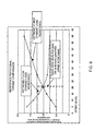
- the Zener diodes D2, D3 are selected such that they will break down (turn on) at the point where the characteristic curve for a low resistance load intersects the characteristic curve for a high resistance load as shown in Fig. 6.
- Zener diode D3 in the negative side circuit 1b turns on so that current flows to the gate of thyristor TY2 and turns on thyristor TY2.
- current from dynamo 2 is shunted from the second output terminal to the first output terminal through thyristor TY2.
- current is blocked by diode D1 so that thyristor TY1 remains off.
- current from the dynamo 2 is shunted through the current bypass circuit 6 and is not delivered to the dynamo load side.
- Fig. 8 is a flow chart of a particular embodiment of a voltage control process for the above circuit.
- Step S1 it is determined whether the voltage generated by the dynamo 2 exceeds a set value, and in Step S2 it is determined whether the voltage generated is equal to or less than the set value.
- These decision steps S1, S2 correspond to determining whether the generated voltage exceeds the breakdown voltage of the Zener diodes D2, D3.
- Step S3 the amount of current passing through the current bypass circuit 6 is reduced.
- the process of Step S3 corresponds to the case where Zener diodes D2, D3 are in current blocking mode and thyristors TY1, TY2 are turned off.
- a voltage control circuit comprising a voltage monitoring circuit and a current bypass circuit need not be constructed integrally with the dynamo load 3.
- those components could be situated on separate connection lines between dynamo 2 and dynamo load 3.
- the voltage control circuit 1 also could be connected to a generating device 2a within dynamo 2 as shown in Fig. 10. This reduces the amount of space occupied by the device in the overall system.
Landscapes
- Engineering & Computer Science (AREA)
- Power Engineering (AREA)
- Mechanical Engineering (AREA)
- Control Of Eletrric Generators (AREA)
Abstract
Description
Claims (17)
- A device (1) for preventing high voltage from acting on a load driven (3) by a bicycle dynamo (2), wherein the device comprises:wherein the sensor circuit (5) provides a control signal when the operating signal passes a threshold value; anda sensor circuit (5) that senses an operating signal derived from the dynamo (2), wherein the operating signal corresponds to a voltage generated by the dynamo (2);
a control circuit (6) operatively coupled to the sensor circuit (5) and adapted to be coupled between the dynamo (2) and the load (3) to control the current delivered to the load (3) in response to the control signal. - The device according to claim 1 wherein the control circuit (6) shunts current away from the load (3) in response to the control signal.
- The device according to claim 1 wherein the sensor circuit (5) is structured to sense a voltage generated by the dynamo (2).
- The device according to claim 1 wherein the sensor circuit (5) is structured to sense a frequency generated by the dynamo (2).
- The device according to claim 1 wherein the sensor circuit (5) includes a Zener diode that receives the operating signal derived from the dynamo (2).
- The device according to claim 5 wherein the Zener diode provides the control signal.
- The device according to claim 6 wherein the control circuit (6) includes a thyristor that receives the control signal from the Zener diode.
- The device according to claim 1 wherein the control circuit (6) includes a thyristor that receives the control signal from the sensor circuit (5).
- The device according to claims 7 or 8 wherein the control signal is applied to a gate terminal of the thyristor.
- The device according to claims 8 or 9 wherein the thyristor is adapted to be coupled between first and second output terminals of the dynamo (2).
- The device according to claims 5 or 10 wherein the Zener diode is adapted to be coupled between the first and second output terminals of the dynamo (2).
- The device according to claim 1 wherein the sensor circuit (5) and the control circuit (6) are integrally constructed with the load (3).
- The device according to claim 1 wherein the sensor circuit(5) and the control circuit (6) together are adapted to be coupled between the dynamo (2) and the load (3).
- The device according to claim 1 wherein the sensor circuit (5) and the control circuit (6) are integrally constructed with the dynamo (2).
- The device according to claim 1 wherein the sensor circuit (5) comprises:wherein the control circuit (6) comprises:a positive side sensor circuit that senses a first operating signal derived from a positive cycle of the dynamo (2); anda negative side sensor circuit that senses a second operating signal derived from a negative cycle of the dynamo (2); anda positive side control circuit (1a) that controls the current delivered to the load (3) during the positive cycle of the dynamo (2); anda negative side control circuit (1b) that controls the current delivered to the load (3) during the negative cycle of the dynamo (2).
- The device according to claim 15 wherein the positive side sensor circuit comprises a first Zener diode that provides a positive cycle control signal, wherein the negative side sensor circuit comprises a second Zener diode that provides a negative cycle control signal, wherein the positive side control circuit (1a) comprises a first thyristor that receives the positive cycle control signal, and wherein the negative side control circuit (1b comprises a second thyristor that receives the negative cycle control signal.
- The device according to claim 16 wherein the first Zener diode provides the positive cycle control signal to a gate terminal of the first thyristor, and wherein the second Zener diode provides the negative cycle control signal to a gate terminal of the second thyristor.
Applications Claiming Priority (2)
| Application Number | Priority Date | Filing Date | Title |
|---|---|---|---|
| JP2002201117 | 2002-07-10 | ||
| JP2002201117A JP2004088812A (en) | 2002-06-27 | 2002-07-10 | Overvoltage protection device for bicycle dynamo |
Publications (3)
| Publication Number | Publication Date |
|---|---|
| EP1381137A2 true EP1381137A2 (en) | 2004-01-14 |
| EP1381137A3 EP1381137A3 (en) | 2006-10-04 |
| EP1381137B1 EP1381137B1 (en) | 2009-05-13 |
Family
ID=29728455
Family Applications (1)
| Application Number | Title | Priority Date | Filing Date |
|---|---|---|---|
| EP03015492A Expired - Lifetime EP1381137B1 (en) | 2002-07-10 | 2003-07-09 | Voltage control circuit for a bicycle dynamo |
Country Status (5)
| Country | Link |
|---|---|
| US (1) | US6788030B2 (en) |
| EP (1) | EP1381137B1 (en) |
| CN (2) | CN101635554A (en) |
| DE (1) | DE60327582D1 (en) |
| TW (1) | TWI244448B (en) |
Cited By (1)
| Publication number | Priority date | Publication date | Assignee | Title |
|---|---|---|---|---|
| EP2717404A1 (en) * | 2012-10-08 | 2014-04-09 | AAT Alber Antriebstechnik GmbH | Protection circuit for electric wheelchairs |
Families Citing this family (3)
| Publication number | Priority date | Publication date | Assignee | Title |
|---|---|---|---|---|
| JP2005349995A (en) * | 2004-06-11 | 2005-12-22 | Shimano Inc | Bicycle electrical equipment protection circuit |
| CN107643546B (en) * | 2017-10-31 | 2024-02-23 | 吉林大学 | A magnetometer based on statistical superposition method |
| CN110380394A (en) * | 2019-08-20 | 2019-10-25 | 珠海格力电器股份有限公司 | Direct current bus overvoltage crowbar, converter and air conditioner |
Family Cites Families (11)
| Publication number | Priority date | Publication date | Assignee | Title |
|---|---|---|---|---|
| JPS5687384A (en) * | 1979-12-18 | 1981-07-15 | Fujitsu Ltd | Light emitting diode type display lamp |
| US4380727A (en) * | 1981-03-25 | 1983-04-19 | Thomas H. Rudd | Voltage regulator system for motorcycles and the like |
| US4894602A (en) * | 1988-06-02 | 1990-01-16 | Brunswick Corporation | Overvoltage protection system for marine ignition and regulator circuitry |
| DE3832109A1 (en) * | 1988-09-21 | 1990-03-22 | Juergen Munz | Luminaire |
| US4882531A (en) * | 1988-09-26 | 1989-11-21 | Motorola Inc. | Integrated circuit voltage regulator and charging system |
| DK0460585T3 (en) * | 1990-06-07 | 1994-03-07 | Bisy Bike Systems Ind Fertigun | Bicycle light system with alternator |
| EP0709944A1 (en) * | 1994-10-31 | 1996-05-01 | STMicroelectronics S.r.l. | Charge voltage regulator for a battery |
| DE19830792B4 (en) * | 1997-07-16 | 2009-08-27 | Busch & Müller KG | Circuit arrangement with light-emitting diode, in particular for a bicycle light |
| JP3932632B2 (en) * | 1997-11-28 | 2007-06-20 | 株式会社デンソー | Vehicle power supply |
| JP2002187584A (en) * | 2000-12-22 | 2002-07-02 | Shimano Inc | Drive control circuit for electric bicycle unit |
| JP3520058B2 (en) * | 2001-06-11 | 2004-04-19 | 三菱電機株式会社 | Control device for vehicle generator |
-
2003
- 2003-06-24 TW TW092117150A patent/TWI244448B/en not_active IP Right Cessation
- 2003-07-08 US US10/616,253 patent/US6788030B2/en not_active Expired - Lifetime
- 2003-07-09 CN CN200910165920A patent/CN101635554A/en active Pending
- 2003-07-09 DE DE60327582T patent/DE60327582D1/en not_active Expired - Lifetime
- 2003-07-09 CN CNA031471986A patent/CN1472881A/en active Pending
- 2003-07-09 EP EP03015492A patent/EP1381137B1/en not_active Expired - Lifetime
Cited By (1)
| Publication number | Priority date | Publication date | Assignee | Title |
|---|---|---|---|---|
| EP2717404A1 (en) * | 2012-10-08 | 2014-04-09 | AAT Alber Antriebstechnik GmbH | Protection circuit for electric wheelchairs |
Also Published As
| Publication number | Publication date |
|---|---|
| US6788030B2 (en) | 2004-09-07 |
| TWI244448B (en) | 2005-12-01 |
| EP1381137A3 (en) | 2006-10-04 |
| CN101635554A (en) | 2010-01-27 |
| CN1472881A (en) | 2004-02-04 |
| EP1381137B1 (en) | 2009-05-13 |
| DE60327582D1 (en) | 2009-06-25 |
| US20040052017A1 (en) | 2004-03-18 |
| TW200403168A (en) | 2004-03-01 |
Similar Documents
| Publication | Publication Date | Title |
|---|---|---|
| CN1360386B (en) | Drive control circuit for bicycle electric unit | |
| JP3914004B2 (en) | Overcurrent detection / protection device for semiconductor elements | |
| EP2216876A1 (en) | Power supply apparatus for vehicles | |
| US6118253A (en) | Charging and discharging control circuit and charging type power supply device | |
| JP3829288B2 (en) | Charger | |
| EP1862348A1 (en) | Motor control apparatus and on-vehicle motor drive system | |
| KR101010506B1 (en) | Inverter control method | |
| KR940006839A (en) | Brake Control of Electric Motor Vehicles | |
| JP3627047B2 (en) | Voltage controller that controls the output voltage of the generator | |
| EP1381137B1 (en) | Voltage control circuit for a bicycle dynamo | |
| JP4196927B2 (en) | Vehicle power generation control device | |
| JP5838770B2 (en) | Driving device for power switching element | |
| US5039931A (en) | 12 Volt battery charger circuit | |
| KR102231539B1 (en) | Method for operating an energy supply unit for an on-board power system of a motorvehicle | |
| JP2014138531A (en) | Power supply device, power supply control method, and program thereof | |
| JP4391513B2 (en) | Control device for vehicle alternator | |
| CN1878685B (en) | tram control device | |
| WO2015190421A1 (en) | Electronic control device | |
| JP2014161195A (en) | Dc power supply device | |
| WO2018225235A1 (en) | Control device for dc-dc converter | |
| US7417407B1 (en) | Circuit with a switch for charging a battery in a battery capacitor circuit | |
| JP2004088812A (en) | Overvoltage protection device for bicycle dynamo | |
| JP2837307B2 (en) | Vehicle charging generator | |
| JP4538990B2 (en) | Voltage control device | |
| JP6477370B2 (en) | Switch signal input circuit |
Legal Events
| Date | Code | Title | Description |
|---|---|---|---|
| PUAI | Public reference made under article 153(3) epc to a published international application that has entered the european phase |
Free format text: ORIGINAL CODE: 0009012 |
|
| AK | Designated contracting states |
Kind code of ref document: A2 Designated state(s): AT BE BG CH CY CZ DE DK EE ES FI FR GB GR HU IE IT LI LU MC NL PT RO SE SI SK TR |
|
| AX | Request for extension of the european patent |
Extension state: AL LT LV MK |
|
| RAP1 | Party data changed (applicant data changed or rights of an application transferred) |
Owner name: SHIMANO INC. |
|
| PUAL | Search report despatched |
Free format text: ORIGINAL CODE: 0009013 |
|
| AK | Designated contracting states |
Kind code of ref document: A3 Designated state(s): AT BE BG CH CY CZ DE DK EE ES FI FR GB GR HU IE IT LI LU MC NL PT RO SE SI SK TR |
|
| AX | Request for extension of the european patent |
Extension state: AL LT LV MK |
|
| RIC1 | Information provided on ipc code assigned before grant |
Ipc: B62J 6/00 20060101ALI20060825BHEP Ipc: H02J 7/14 20060101AFI20031105BHEP Ipc: H02H 9/04 20060101ALI20060825BHEP |
|
| 17P | Request for examination filed |
Effective date: 20061026 |
|
| AKX | Designation fees paid |
Designated state(s): DE FR IT NL |
|
| 17Q | First examination report despatched |
Effective date: 20070604 |
|
| GRAP | Despatch of communication of intention to grant a patent |
Free format text: ORIGINAL CODE: EPIDOSNIGR1 |
|
| GRAS | Grant fee paid |
Free format text: ORIGINAL CODE: EPIDOSNIGR3 |
|
| GRAA | (expected) grant |
Free format text: ORIGINAL CODE: 0009210 |
|
| AK | Designated contracting states |
Kind code of ref document: B1 Designated state(s): DE FR IT NL |
|
| REF | Corresponds to: |
Ref document number: 60327582 Country of ref document: DE Date of ref document: 20090625 Kind code of ref document: P |
|
| PLBE | No opposition filed within time limit |
Free format text: ORIGINAL CODE: 0009261 |
|
| STAA | Information on the status of an ep patent application or granted ep patent |
Free format text: STATUS: NO OPPOSITION FILED WITHIN TIME LIMIT |
|
| 26N | No opposition filed |
Effective date: 20100216 |
|
| REG | Reference to a national code |
Ref country code: FR Ref legal event code: ST Effective date: 20100331 |
|
| PG25 | Lapsed in a contracting state [announced via postgrant information from national office to epo] |
Ref country code: FR Free format text: LAPSE BECAUSE OF NON-PAYMENT OF DUE FEES Effective date: 20090731 |
|
| PG25 | Lapsed in a contracting state [announced via postgrant information from national office to epo] |
Ref country code: IT Free format text: LAPSE BECAUSE OF FAILURE TO SUBMIT A TRANSLATION OF THE DESCRIPTION OR TO PAY THE FEE WITHIN THE PRESCRIBED TIME-LIMIT Effective date: 20090513 |
|
| PGFP | Annual fee paid to national office [announced via postgrant information from national office to epo] |
Ref country code: NL Payment date: 20160610 Year of fee payment: 14 |
|
| REG | Reference to a national code |
Ref country code: NL Ref legal event code: MM Effective date: 20170801 |
|
| PG25 | Lapsed in a contracting state [announced via postgrant information from national office to epo] |
Ref country code: NL Free format text: LAPSE BECAUSE OF NON-PAYMENT OF DUE FEES Effective date: 20170801 |
|
| PGFP | Annual fee paid to national office [announced via postgrant information from national office to epo] |
Ref country code: DE Payment date: 20180626 Year of fee payment: 16 |
|
| REG | Reference to a national code |
Ref country code: DE Ref legal event code: R119 Ref document number: 60327582 Country of ref document: DE |
|
| PG25 | Lapsed in a contracting state [announced via postgrant information from national office to epo] |
Ref country code: DE Free format text: LAPSE BECAUSE OF NON-PAYMENT OF DUE FEES Effective date: 20200201 |