EP1381075A2 - Image sensor unit - Google Patents
Image sensor unit Download PDFInfo
- Publication number
- EP1381075A2 EP1381075A2 EP03015511A EP03015511A EP1381075A2 EP 1381075 A2 EP1381075 A2 EP 1381075A2 EP 03015511 A EP03015511 A EP 03015511A EP 03015511 A EP03015511 A EP 03015511A EP 1381075 A2 EP1381075 A2 EP 1381075A2
- Authority
- EP
- European Patent Office
- Prior art keywords
- light emitting
- electrode
- image sensor
- sensor unit
- lamp
- Prior art date
- Legal status (The legal status is an assumption and is not a legal conclusion. Google has not performed a legal analysis and makes no representation as to the accuracy of the status listed.)
- Withdrawn
Links
Images


Classifications
-
- H—ELECTRICITY
- H04—ELECTRIC COMMUNICATION TECHNIQUE
- H04N—PICTORIAL COMMUNICATION, e.g. TELEVISION
- H04N1/00—Scanning, transmission or reproduction of documents or the like, e.g. facsimile transmission; Details thereof
- H04N1/04—Scanning arrangements, i.e. arrangements for the displacement of active reading or reproducing elements relative to the original or reproducing medium, or vice versa
- H04N1/19—Scanning arrangements, i.e. arrangements for the displacement of active reading or reproducing elements relative to the original or reproducing medium, or vice versa using multi-element arrays
-
- H—ELECTRICITY
- H04—ELECTRIC COMMUNICATION TECHNIQUE
- H04N—PICTORIAL COMMUNICATION, e.g. TELEVISION
- H04N1/00—Scanning, transmission or reproduction of documents or the like, e.g. facsimile transmission; Details thereof
- H04N1/024—Details of scanning heads ; Means for illuminating the original
- H04N1/028—Details of scanning heads ; Means for illuminating the original for picture information pick-up
- H04N1/02815—Means for illuminating the original, not specific to a particular type of pick-up head
- H04N1/02845—Means for illuminating the original, not specific to a particular type of pick-up head using an elongated light source, e.g. tubular lamp, LED array
-
- H—ELECTRICITY
- H01—ELECTRIC ELEMENTS
- H01J—ELECTRIC DISCHARGE TUBES OR DISCHARGE LAMPS
- H01J61/00—Gas-discharge or vapour-discharge lamps
- H01J61/02—Details
- H01J61/54—Igniting arrangements, e.g. promoting ionisation for starting
-
- H—ELECTRICITY
- H01—ELECTRIC ELEMENTS
- H01J—ELECTRIC DISCHARGE TUBES OR DISCHARGE LAMPS
- H01J65/00—Lamps without any electrode inside the vessel; Lamps with at least one main electrode outside the vessel
- H01J65/04—Lamps in which a gas filling is excited to luminesce by an external electromagnetic field or by external corpuscular radiation, e.g. for indicating plasma display panels
- H01J65/042—Lamps in which a gas filling is excited to luminesce by an external electromagnetic field or by external corpuscular radiation, e.g. for indicating plasma display panels by an external electromagnetic field
- H01J65/046—Lamps in which a gas filling is excited to luminesce by an external electromagnetic field or by external corpuscular radiation, e.g. for indicating plasma display panels by an external electromagnetic field the field being produced by using capacitive means around the vessel
-
- H—ELECTRICITY
- H04—ELECTRIC COMMUNICATION TECHNIQUE
- H04N—PICTORIAL COMMUNICATION, e.g. TELEVISION
- H04N1/00—Scanning, transmission or reproduction of documents or the like, e.g. facsimile transmission; Details thereof
- H04N1/024—Details of scanning heads ; Means for illuminating the original
- H04N1/028—Details of scanning heads ; Means for illuminating the original for picture information pick-up
- H04N1/02815—Means for illuminating the original, not specific to a particular type of pick-up head
Definitions
- the light emission control of the external light source 25 is performed by a lighting circuit (not shown), which keeps the external light source 25 in the ON state for a prescribed time prior to activating the light emitting lamp 2.
Landscapes
- Engineering & Computer Science (AREA)
- Physics & Mathematics (AREA)
- Multimedia (AREA)
- Signal Processing (AREA)
- Electromagnetism (AREA)
- Plasma & Fusion (AREA)
- Vessels And Coating Films For Discharge Lamps (AREA)
- Facsimile Heads (AREA)
- Facsimile Scanning Arrangements (AREA)
- Light Sources And Details Of Projection-Printing Devices (AREA)
Abstract
Description
- The present invention relates to an image sensor unit, and more particularly, to an improved structure of a continuously dischargeable light source used in the image sensor unit, which can improve the starting characteristic of the light source for achieving stable glow discharge (that is, so-called continuous electric discharge).
- In general, photocopy machines, facsimile machines, scanners, and other image-reproducing machines use an image sensor unit to optically read the image from the original. Some image sensor units use a certain type of light source that makes use of continuous electric discharge occurring between electrodes, instead of utilizing the light emitting phenomenon of thermal particles from a filament.
- One example of the light source making use of the continuous electric discharge comprises a light-emitting body made of a dielectric material and shaped as an airtight container, filled with xenon gas, for example under a prescribed vacuum atmosphere. In the container, a fluorescent material layer is provided, except for a certain region, and two electrodes are arranged so as to face each other with a space between them. When a discharge starting voltage is applied between the electrodes, a strong electric field is generated between them, and the gas filled in the container is ionized and excited to produce ultraviolet rays. The ultraviolet rays cause the fluorescent material layer to emit light, functioning as the light source.
- If the object to be optically scanned, such as an original, has a flat surface, a plate glass with a flat surface is used in the image sensor unit to hold the scanned surface of the original. In this case, the light emitting structure described above is placed below the plate glass so as to irradiate the original from the bottom.
- It is important for the above-described type of image sensor unit to reliably provide the starting characteristic of the light source. Accordingly, it is proposed to create a localized area of the strong electric field effect to enhance the electric discharge efficiency, thereby securing continuous light emission across the entire range (see, for example, JPA 11-283579). It is also proposed to use an additional light source to irradiate the light emitting body in order to ionize and excite the gas filled in the light emitting body (see, for example, JPA 4-106896). Still another proposal is to mix a material that easily emits electrons in the fluorescent material used in the light emitting body, instead of irradiating the light emitting body (see, for example, JPA 2000-156203 and JPA 2001-123988). Yet another proposal is that a portion of the fluorescent layer be removed so as to allow initial electrons to emit from this removed portion for the purpose of starting ionization and excitation of the gas (see, for example, JPA 2001-102004). The emission of the initial electrons is compared to a "small flame" for sequentially causing ionization and excitation to achieve continuous electric discharge.
- However, there are several problems in the above-described prior art techniques of enhancing the starting characteristic.
- First, the conventional method of generating a strong electric field requires auxiliary electrodes to generate such a strong electric field, and the configuration of the light emitting body, including the ordinary electrodes, has to be changed. This results in increased cost. Particularly, if the height of the discharge space defined by the light emitting body is insufficient, the insulating distance of the auxiliary electrodes cannot be maintained reliably. This drawback may cause dielectric breakdown, and therefore, cause the light source to return to the dark state, causing dark current. In addition, the lighting circuit may be damaged, or the inside of the image sensor unit may be burned. Consequently, the starting characteristic cannot be improved efficiently.
- Second, with the prior art technique using an additional light source, or mixing a material that easily emits electrons in the fluorescent layer, the emitted electrons are likely to be captured if the purity of the gas filled in the light emitting body is degraded. Since this phenomenon adversely affects the efficiency of the ionization and the excitation of the gas, the purity of the gas has to be maintained high. In addition, when a portion of the electrode is exposed, sputtering occurs on the exposed surface of the electrode, and the illumination of the light source decreases.
- Third, with the prior art technique of removing a portion of the fluorescent material layer to expose the underlying layer or material to the gas, the quantify of light may become uneven or insufficient within the scanning range of the original, which is the scanning target of the image sensor unit. This may cause the S/N ratio to be degraded. In addition, since most of the surface of the light emitting body made of a dielectric is covered with the fluorescent material layer, the voltage applied between the electrodes has to be increased in order to guarantee initial emission of electrons. It is difficult for the light source of this technique to maintain electric discharge continuously along the longitudinal axis of the light emitting body, even if weak electric discharge has occurred at the exposed portion, and in the worst case, electric discharge may stop.
- Therefore, it is an object of the present invention to overcome the above-described problems in the conventional image sensor units, especially in the light emitting part making use of continuous electric discharge, and to provide an image sensor unit with an improved starting characteristic that can prevent undesirable dielectric breakdown and cost increase. This image sensor unit has a light emitting body that is capable of providing continuous electric discharge across the entire scanning area of the light emitting body, while preventing the degradation of the S/N ratio.
- To achieve the object, an image sensor unit having an electric discharge light emitting lamp for producing an illumination beam is provided. The lamp comprises a first electrode and a second electrode facing each other and defining a discharge space between them along the longitudinal axis of the lamp. A first light emitting layer and a second light emitting layer are provided in the discharge space so as to face each other and to cover the first and second electrodes, respectively. A dielectric material is inserted between the first electrode and the first light emitting layer, and between the second electrode and the second light emitting layer. At least one of the first and second light emitting layers is arranged so as to define an uncovered region, in which at least one of the dielectric material, the first electrode, and the second electrode is exposed to the discharge space.
- When a voltage is applied between the first and second electrodes, initial electrons emit from the uncovered region, which causes electric discharge in the discharge space in which electrically charged particles collide each other. Ultraviolet rays generated from the electric discharge illuminates the light emitting layer that faces the discharge space, causing the light emitting layer to emit an illumination beam.
- The uncovered region, which is not covered with the light emitting layer, extends from one end of the lamp continuously or discontinuously along the longitudinal axis of the lamp.
- It is desirable for the uncovered region to be arranged outside the scanning area of the image sensor unit.
- Preferably, in the uncovered region, a photoemission material that easily emits photoelectrons is contained.
- If the dielectric material is exposed to the discharge space in the uncovered region, a photoemission material is contained in the exposed portion of the dielectric material.
- Alternatively, if the first or second electrode is exposed to the discharge space in the uncovered region, a photoemission material is contained in the exposed portion of the first or second electrode.
- Preferably, the image sensor unit further comprises an external light source configured to irradiate the uncovered region of the lamp.
- Other objects, features, and advantages of the present invention will become more apparent from the following detailed description when read in conjunction with the accompanying drawings, in which:
- FIG. 1 is a schematic perspective view of the image sensor unit according to an embodiment of the present invention;
- FIG. 2 is a schematic diagram of the image sensor used to explain the scanning operation of the image sensor unit shown in FIG. 1;
- FIG. 3 is a vertical cross-sectional view of the light emitting lamp used in the image sensor unit shown in FIG. 1, taken along the longitudinal axis of the light emitting lamp;
- FIG. 4 is a perspective view of the light emitting lamp shown in FIG. 3;
- FIG. 5 is a plan view of the first part of the light emitting lamp of FIG. 3 viewed in the direction indicated by the arrows (5) in FIG. 3, illustrating the arrangement of the uncovered regions;
- FIG. 6 illustrates the positional relation between the light emitting layer and the insulating layer positioned below the light emitting layer, which is used to explain the arrangement of the uncovered regions shown in FIG. 5;
- FIG. 7 illustrates the positional relation between the light emitting layer and the internal electrode, which is used to explain the arrangement of the uncovered regions shown in FIG. 5;
- FIG. 8 is plan view of the second part of the light emitting lamp of FIG. 3 viewed in the direction indicated by the arrows (8), illustrating the arrangement of the uncovered regions; and
- FIG. 9 illustrates the positional relation between the light emitting layer and the external electrode, which is used to explain the arrangement of the uncovered regions shown in FIG. 8.
-
- The preferred embodiments of the present invention will now be described in detail with reference to the attached drawings.
- FIG. 1 is a schematic perspective view of the image sensor unit according to an embodiment of the present invention. The
image sensor unit 1 comprises acasing unit 1A, in which alight emitting lamp 2, a SELFOClens array 3 that defines a focusing light transmission body, and acircuit element substrate 4 on which a set of light-receiving elements are accommodated. - In the scanning operation of the
image sensor unit 1, the original O placed on the mount, such as thecontact glass 5, is irradiated by the illumination light emitted from the electric discharge light emitting source (or the lamp) 2, as indicated by the arrow of the dashed line in FIG. 2. The light reflected from the original O is focused onto the light-receivingelement 4A formed on thecircuit element substrate 4, via theSELFOC lens array 3, thereby reading the images or information from the original O. Thenumerical reference 6 denotes the connector for electrically connecting thecircuit.element substrate 4 to an external controller (not shown). - FIG. 3 and the subsequent figures illustrate the structure of the
light emitting lamp 2. - FIG. 3 is a vertical cross-sectional view of the
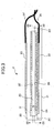
light emitting lamp 2 taken along the longitudinal axis thereof. Thelight emitting lamp 2 comprises afirst plate 2A and asecond plate 2B, each being transparent to light and made of a dielectric containing a photoemission material, such as an oxide of an alkaline-earth metal. The first and secondtransparent plates member 2C (e.g., frit glass) in an airtight manner to form a lamp body. In the lamp body, adischarge space 2D is formed betweenelectrodes discharge space 2D is set to the prescribed vacuum atmosphere, and filled with a discharge gas, such as xenon (Xe) gas. - The
internal electrode 22 is provided on thefirst plate 2A so as to face thedischarge space 2D. Theinternal electrode 22 is covered with an insulatinglayer 21 for electrical insulation, on which a light-emittinglayer 20 made of a fluorescent material is placed. The inner face of thesecond plate 2B is furnished with a light emitting layer 20' made of a fluorescent material, facing thedischarge space 2D. Theexternal electrode 23 is provided on the outer face of thesecond plate 2B. Theexternal electrode 23 is positioned so as to face theinternal electrode 22 formed on thefirst plate 2A via thesecond plate 2B and thedischarge space 2D. -
Harnesses 24 and 24' are soldered to theinternal electrode 22 and theexternal electrode 23, respectively. Theharnesses 24 and 24' are connected to the external lighting circuit (not shown) at the other ends. Although not shown, theexternal electrode 23 may be furnished with a grounding structure, or alternatively, covered with an insulating film, for the purpose of safe operation and shielding external noise. - The
light emitting lamp 2 of this example is designed so as to emit light from a plane perpendicular to the top face of thesecond plate 2B on which theexternal electrode 23 is provided, as indicated by the dashed arrow R in FIG. 4. - Certain regions of the inner faces of the first and
second plates light emitting layers 20 and 20', as indicated by symbols D and D', respectively, along the longitudinal axis of thelight emitting lamp 2. These regions are referred to as the uncovered regions D and D'. Portions of theelectrodes layer 21, and/or theelectrode 22, and/or theelectrode 23 are exposed to thedischarge space 2D, without being covered with thelight emitting layer 20 or 20'. - The uncovered regions D and D' are located at or near the end of the
light emitting lamp 2. The uncovered regions D and D' may extend from the end of thelight emitting lamp 2 continuously along the longitudinal axis of thelight emitting lamp 2, or alternatively, they may be located locally or discontinuously in thelight emitting lamp 2. In either case, if a large-sized uncovered region is produced, such a large region is arranged outside the scanning area in order to prevent the light quantity from decreasing locally or from becoming uneven in the scanning range. This arrangement can also prevent the S/N ratio from degrading during the operation of optically reading an original. - FIG. 5 illustrates a plan view of the
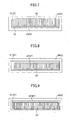
first plate 2A viewed from the arrow (5) shown in FIG. 3. In this example, the uncovered region D1 is located at one end of thelight emitting layer 20, and another uncovered region D2 extends from the region D1 along the lengthwise edge of thelight emitting layer 20 parallel to the longitudinal axis thereof. A portion of the insulatinglayer 21 and/or a portion of theinternal electrode 22 falls in the uncovered regions D1 and/or D2, which will be explained below. - FIG. 6 is a plan view of the
first plate 2A, illustrating the positional relation between the light emittinglayer 20 and the insulatinglayer 21 formed on thefirst plate 2A. A portion of the insulatinglayer 21 is exposed to thedischarge space 2D because thelight emitting layer 20 does not cover the insulatinglayer 21 in the uncovered regions D1 and D2. In this example, the underlying internal electrode 23 (not shown in FIG. 6) is formed so as to project from thelight emitting layer 20, but not to project from the insulatinglayer 21. - A photoemission material, such as an oxide of an alkaline-earth metal, may be mixed into the exposed portion or the entirety of the insulating
layer 21 in order to guarantee a sufficient quantity of light in the uncovered regions D1 and D2. Alternatively; a photoemission material layer may be formed on the exposed surface of the insulatinglayer 21. - FIG. 7 is a plan view of another example of the
first plate 2A, illustrating the positional relation between the light emittinglayer 20 and theinternal electrode 22 formed on thefirst plate 2A. In this example, the insulatinglayer 21 is covered with thelight emitting layer 20, and is not exposed to thedischarge space 2D. Theinternal electrode 22 projects from thelight emitting layer 20 at one end of thelight emitting layer 20 within the uncovered region D1, and simultaneously projects from thelight emitting layer 20 along a lengthwise edge thereof in the uncovered region D2. These projecting portions of theinternal electrode 22 are exposed to thedischarge space 2D. Consequently, the voltage applied between theinternal electrode 22 and theexternal electrode 23 can be maintained low. A photoemission material may be mixed into the electrode material, or a photoemission material layer may be formed on the exposed surface of the internal,electrode 22. - FIG. 8 illustrates a plan view of the
second plate 2B viewed from the arrow (8) shown in FIG. 3. The uncovered region D1' is located at one end of the light emitting layer 20', and another uncovered region D2' extends from the uncovered region D1' along a lengthwise edge of the light emitting layer 20' in parallel to the longitudinal axis thereof. - FIG. 9 illustrates the positional relation between the light emitting layer 20' and the
external electrode 23 formed on the outer surface of thesecond plate 2B. Theexternal electrode 23 projects from the light emitting layer 20' formed inside thesecond plate 2B, and therefore, faces thedischarge space 2D via the transparentsecond plate 2B in the uncovered regions D1' and D2'. - In the uncovered regions D1' and D2', the dielectric that forms the
second plate 2B is exposed to thedischarge space 2D. Because of the photoemission material mixed into thesecond plate 2B, the light quantity can be prevented from dropping in the uncovered regions D1' and D2'. - In the uncovered regions D and D' in which the
light emitting layer 20 and 20' are not formed, the exposed portions of theplate layer 21 directly face thedischarge space 2D. These exposed portions contain a photoemission material, such as an oxide of an alkaline-earth metal. The photoemission material may also be mixed into the internal electrode in the uncovered regions D and D'. - In this manner, at least one of the group consisting of the plate material, the insulating
layer 21, and theelectrode 22 are exposed directly to thedischarge space 2D in the uncovered regions D and D' that are not covered with thelight emitting layers 20 and 20' inside thelight emitting lamp 2. Consequently, when a voltage is applied between theelectrodes light emitting layers 20 and 20'. Consequently, the starting characteristic of the light emitting lamp can be improved. - Next, another embodiment of the present invention will be described.
- In this embodiment, an additional light source is used to illuminate the uncovered regions that do not include the light emitting layer.
- As illustrated in FIG. 1, FIG. 2 and FIG. 4, an external light source 25 (such as an LED, a midget lamp, or an EL) is placed near the
light emitting lamp 2. In the preferred example, a blue LED capable of emitting a short-wavelength light with high photon energy is used. The blue LED is arranged so that the light beam is easily guided onto the uncovered regions. - The light emission control of the external
light source 25 is performed by a lighting circuit (not shown), which keeps the externallight source 25 in the ON state for a prescribed time prior to activating thelight emitting lamp 2. - If the external
light source 25 is turned on, the light beam emitted from the externallight source 25 irradiates the uncovered regions D and D' of thelight emitting lamp 2, which are not covered with thelight emitting layers 20 and 20', respectively. In response to the irradiation, initial electrons emit from the photoemission material located at the surface exposed directly to thedischarge space 2D. In the electric field produced between theelectrodes discharge space 2D, while amplifying the ionization of the discharge gas, and finally reach the light emitting layer or the uncovered region on the opposite electrode side. When ultraviolet rays generated due to the ionization and the excitation of the discharge gas strike the light emitting layer, satisfactory light emission is achieved. - Depending on the polarity of the voltage at the electrode, the electrons and ions generated from the ionization and excitation of the discharge gas are absorbed in the light emitting layer, and the underlying insulating layer and the electrode. In this case, the electric field between the electrodes may be weakened, and the electric discharge cannot be sufficiently maintained. To prevent this situation, a voltage with an opposite polarity is generally applied between the electrodes to inverse the direction of the electric field in a periodic manner. However, it is generally difficult for those electrons absorbed in the light emitting layer to emit to the discharge space unless the inverted electric field is made strong. Accordingly, it may take a long time for the electron to receive energy sufficient to emit. This means that it takes a long time before electric discharge starts in the discharge gas. In this case, the polarity of the electric field is again inverted to the previous state, without producing light emission during the inverted period.
- This undesirable situation can be effectively prevented by the present invention because the uncovered regions D2 and D2' are formed along the longitudinal axis of the
light emitting layer 20 and 20'. In the uncovered regions D2 and D2', the electrons can emit promptly from the insulating layer or the electrode at a lower voltage, as compared with electron emission from the light emitting layer, even if the polarity of the voltage is switched. Thus, light emission can be guaranteed during the discharge period. - In general, as the polarity inversion is repeated, the number of electrons emitted into the discharge gas increases, and consequently, the light emission phenomenon occurs in the entirety of the light emitting lamp. However, if the absorption of the electrons in the light emitting layer increases, it generally becomes difficult for the prior art technique to cause the light emitting phenomenon having occurred near the external
light source 25 to spread over the entire space of the lamp. In contrast, with the present invention, the uncovered regions D2 and D2' allow electric discharge to easily and promptly spread over the entire space of the lamp, thereby improving the starting characteristic of thelight emitting lamp 2. - In the above-described example, the uncovered regions D and D' in which the
light emitting layers 20 and 20' are not formed are provided at an end opposite to the end portion at which theharnesses 24 and 24' are connected to theelectrodes second plates - In conclusion, photoemission is performed promptly in response to application of voltage between the electrodes of the light emitting lamp, because the light emitting layer is arranges so as to expose a certain region (referred to as an "uncovered region") of the underlying layer to the discharge space. The initial electrons cause electric discharge in the discharge space, where electrically charged particles collide with each other. In the exposed region or the uncovered region, at least one of the first or second plate made of a dielectric material, the insulating layer, and the electrode is exposed to the discharge space. With this arrangement, emission of the initial electron can start more quickly than in the conventional method. This arrangement can also prevent the ionized electrons, which is generated by irradiation or external faint light, or by electric discharge in the gas filling the discharge space, from being absorbed deep into the light emitting layer. Consequently, photoelectrons can emit to the discharge space easily under application of an inverted electric field at a low voltage. The initial emission of photoelectrons in the low-voltage inverted electric field functions as a "small flame", and it hastens light emission in the other area covered with the light emitting layer. The fabrication cost of the light emitting lamp can be maintained low because of the simple structure, in which a portion of the light emitting layer made of, for example, a fluorescent material, is removed within the area facing the discharge space in which electrically charged particles collide with other particles.
- Second, the uncovered region, in which the light emitting layer is not formed, extends from an end of the electric discharge light emitting lamp continuously or discontinuously along the longitudinal axis of the lamp. This arrangement promotes the electric field to act on the other regions, causing the "small flame" to run and extend to the other regions. If the uncovered region is formed continuously along the longitudinal axis of the electric discharge light emitting lamp, the "small flame" is generated across the length of the light emitting layer, which can hasten the start of light emission from the light emitting layer.
- Third, if the uncovered region includes a large-sized region, such a large-sized region is located outside the target scanning area in order to prevent the S/N ratio from degrading during the optical reading. This arrangement is advantageous as compared with the case in which the uncovered region is arranged in the scanning area and light quantity becomes insufficient or uneven.
- Fourth, since the photoemission material is contained in the uncovered region, the initial emission of photoelectrons can be performed efficiently, hastening electric discharge in the discharge space.
- Fifth, since the uncovered regions face each other across the discharge space inside the lamp body sealed in an airtight manner, emission of photoelectrons from the uncovered region is guaranteed, avoiding the electron leakage from the area to the light emitting layers. Consequently, the starting characteristic can be improved.
- Sixth, by irradiating the uncovered region using an additional light source, emission of photoelectrons from the photoemission material contained in the uncovered region can be promoted, in addition to electric discharge under the application of the electric field. With this arrangement, electric discharge is accelerated by combination of application of the electric field and irradiation from the external light source. Consequently, the starting characteristic can be further improved.
- This patent application is based on and claims the benefit of the earlier filing date of Japanese patent application No. 2002-201756 filed July 10, 2002, the entire contents of which are hereby incorporated by reference.
Claims (12)
- An image sensor unit having an electric discharge light emitting lamp for producing an illumination beam, the lamp comprising a first electrode and a second electrode facing each other and defining a discharge space therebetween along the longitudinal axis of the lamp, wherein:a first light emitting layer and a second light emitting layer are provided in the discharge space so as to face each other and to cover the first and second electrodes, respectively;a dielectric material is inserted between the first electrode and the first light emitting layer, and between the second electrode and the second light emitting layer; andat least one of the first and second light emitting layers is arranged so as to define an uncovered region, in which at least one of the dielectric material, the first electrode, and the second electrode is exposed to the discharge space.
- The image sensor unit according to claim 1, wherein the uncovered region extends from one end of the lamp continuously or discontinuously along the longitudinal axis of the lamp.
- The image sensor unit according to claim 1 or 2, wherein the uncovered region is arranged outside the scanning area of the image sensor unit.
- The image sensor unit according to claim 1 or 2, wherein a photoemission material is contained in the uncovered region.
- The image sensor unit according to claim 4, wherein if the dielectric material is exposed to the discharge space in the uncovered region, a photoemission material is contained in the exposed portion of the dielectric material.
- The image sensor unit according to claim 4, wherein if the first or second electrode is exposed to the discharge space in the uncovered region, a photoemission material is contained in the exposed portion of the first or second electrode.
- The image sensor unit according to claim 1 or 2, further comprising an external light source configured to irradiate the uncovered region of the lamp.
- The image sensor unit according to claim 1 or 2, wherein the lamp further comprises a lamp body consisting of a first part and a second part that are combined together and sealed up to form the discharge space between the first and second electrodes, wherein at least one of the first and second parts is transparent to light and made of said dielectric material.
- The image sensor unit according to claim 8, wherein the first electrode is formed on an inner face of the first part, and the second electrode is formed on an outer face of the second part so as to be parallel to the first electrode.
- The image sensor unit according to claim 9, wherein the first light emitting layer is formed above the first electrode via an insulating layer made of said dielectric material, and at least one of the insulating layer and the first electrode is exposed to the discharge space in the uncovered region.
- The image sensor unit according to claim 9, wherein the second light emitting layer is formed on an inner face of the second part so as to define said uncovered region, the second part is made of said dielectric material, and a portion of the dielectric material of the second part is exposed to the discharge space in the uncovered region.
- The image sensor unit according to claim 1 or 2, wherein the uncovered regions are arranged in the first and second light emitting layers, and face each other across the discharge space.
Applications Claiming Priority (2)
| Application Number | Priority Date | Filing Date | Title |
|---|---|---|---|
| JP2002201756A JP3958131B2 (en) | 2002-07-10 | 2002-07-10 | Image sensor unit |
| JP2002201756 | 2002-07-10 |
Publications (2)
| Publication Number | Publication Date |
|---|---|
| EP1381075A2 true EP1381075A2 (en) | 2004-01-14 |
| EP1381075A3 EP1381075A3 (en) | 2004-02-04 |
Family
ID=29728478
Family Applications (1)
| Application Number | Title | Priority Date | Filing Date |
|---|---|---|---|
| EP03015511A Withdrawn EP1381075A3 (en) | 2002-07-10 | 2003-07-09 | Image sensor unit |
Country Status (6)
| Country | Link |
|---|---|
| US (1) | US7365887B2 (en) |
| EP (1) | EP1381075A3 (en) |
| JP (1) | JP3958131B2 (en) |
| KR (1) | KR100568002B1 (en) |
| CN (1) | CN1231040C (en) |
| TW (1) | TWI221386B (en) |
Families Citing this family (2)
| Publication number | Priority date | Publication date | Assignee | Title |
|---|---|---|---|---|
| US20210393825A1 (en) * | 2020-06-23 | 2021-12-23 | The Boeing Company | Ultraviolet excimer lamp systems and methods |
| JP6896919B1 (en) * | 2020-08-03 | 2021-06-30 | 株式会社クォークテクノロジー | Sterilization lamp |
Citations (2)
| Publication number | Priority date | Publication date | Assignee | Title |
|---|---|---|---|---|
| DE4203594A1 (en) | 1991-04-02 | 1992-10-08 | Samsung Electronic Devices | Light discharge tube - has two electrodes parallel to length of transparent tube, one inside and one outside tube |
| JPH11283579A (en) | 1998-03-30 | 1999-10-15 | Toshiba Lighting & Technology Corp | Internal and external electrode type fluorescent lamps and lighting devices |
Family Cites Families (9)
| Publication number | Priority date | Publication date | Assignee | Title |
|---|---|---|---|---|
| US3275872A (en) * | 1963-07-12 | 1966-09-27 | Gen Electric | Reflector fluorescent lamp |
| US3886396A (en) * | 1971-10-10 | 1975-05-27 | Gen Electric | Fluorescent lamp with protective coating |
| JP3250218B2 (en) * | 1990-08-27 | 2002-01-28 | セイコーエプソン株式会社 | Lighting device and liquid crystal display device |
| CA2059209C (en) * | 1991-02-01 | 1997-05-27 | William J. Council | Rf fluorescent lighting |
| JP2000156203A (en) | 1998-11-17 | 2000-06-06 | Nec Home Electronics Ltd | Cold cathode fluorescent lamp |
| EP1111656A4 (en) * | 1999-06-07 | 2007-03-28 | Toshiba Lighting & Technology | DISCHARGE TUBE, DISCHARGE TUBE DEVICE AND IMAGE READER |
| JP4132474B2 (en) * | 1999-09-30 | 2008-08-13 | ハリソン東芝ライティング株式会社 | Noble gas discharge lamp and lighting device |
| JP2001123988A (en) | 1999-10-21 | 2001-05-08 | Hitachi Ltd | Shaft sealing device for turbo chiller |
| DE10140356A1 (en) * | 2001-08-17 | 2003-02-27 | Patent Treuhand Ges Fuer Elektrische Gluehlampen Mbh | Tubular discharge lamp with ignition aid |
-
2002
- 2002-07-10 JP JP2002201756A patent/JP3958131B2/en not_active Expired - Fee Related
-
2003
- 2003-07-08 TW TW092118628A patent/TWI221386B/en not_active IP Right Cessation
- 2003-07-09 US US10/614,819 patent/US7365887B2/en not_active Expired - Fee Related
- 2003-07-09 EP EP03015511A patent/EP1381075A3/en not_active Withdrawn
- 2003-07-10 KR KR1020030046754A patent/KR100568002B1/en not_active Expired - Fee Related
- 2003-07-10 CN CNB031550118A patent/CN1231040C/en not_active Expired - Fee Related
Patent Citations (2)
| Publication number | Priority date | Publication date | Assignee | Title |
|---|---|---|---|---|
| DE4203594A1 (en) | 1991-04-02 | 1992-10-08 | Samsung Electronic Devices | Light discharge tube - has two electrodes parallel to length of transparent tube, one inside and one outside tube |
| JPH11283579A (en) | 1998-03-30 | 1999-10-15 | Toshiba Lighting & Technology Corp | Internal and external electrode type fluorescent lamps and lighting devices |
Also Published As
| Publication number | Publication date |
|---|---|
| US7365887B2 (en) | 2008-04-29 |
| KR100568002B1 (en) | 2006-04-07 |
| TW200402985A (en) | 2004-02-16 |
| CN1231040C (en) | 2005-12-07 |
| JP3958131B2 (en) | 2007-08-15 |
| TWI221386B (en) | 2004-09-21 |
| US20040075873A1 (en) | 2004-04-22 |
| EP1381075A3 (en) | 2004-02-04 |
| JP2004048291A (en) | 2004-02-12 |
| CN1487723A (en) | 2004-04-07 |
| KR20040005697A (en) | 2004-01-16 |
Similar Documents
| Publication | Publication Date | Title |
|---|---|---|
| KR960000537B1 (en) | Discharge lamp, image display device using the same and discharge lamp producing method | |
| US7365887B2 (en) | Image sensor unit | |
| JP2001243921A (en) | Noble gas discharge lamps and lighting devices | |
| US6441548B1 (en) | Discharging and light emitting device | |
| KR100322057B1 (en) | Surface light source | |
| KR100594914B1 (en) | Discharge light-emitting device and contact image sensor utilizing the same | |
| JP4132474B2 (en) | Noble gas discharge lamp and lighting device | |
| CN101159223A (en) | light emitting device | |
| JP2006098334A (en) | Image reading device | |
| JP2002142083A (en) | Original reader | |
| JPH04248246A (en) | Lighting device and image input device | |
| JPH06314561A (en) | Electric discharge lamp | |
| JPH11283579A (en) | Internal and external electrode type fluorescent lamps and lighting devices | |
| JP2004120743A (en) | Light source | |
| JP2004288475A (en) | Beltlike light emitting device | |
| JPH05190150A (en) | Electric discharge lamp | |
| JPH04248245A (en) | Lighting device and image input device | |
| JP3337942B2 (en) | Image reading device | |
| JPH06163008A (en) | Noble gas discharge lamp | |
| JP3016653B2 (en) | Discharge lamp | |
| KR20060100061A (en) | Induction lamps for scanners and copiers | |
| JP2003036814A (en) | Discharge lamps and lighting devices | |
| JPH0229157A (en) | Color picture reader | |
| JPS61284163A (en) | Illuminating device with fluorescent tube for original reading | |
| JPH05227377A (en) | Original lighting light source |
Legal Events
| Date | Code | Title | Description |
|---|---|---|---|
| PUAI | Public reference made under article 153(3) epc to a published international application that has entered the european phase |
Free format text: ORIGINAL CODE: 0009012 |
|
| PUAL | Search report despatched |
Free format text: ORIGINAL CODE: 0009013 |
|
| 17P | Request for examination filed |
Effective date: 20030709 |
|
| AK | Designated contracting states |
Kind code of ref document: A2 Designated state(s): AT BE BG CH CY CZ DE DK EE ES FI FR GB GR HU IE IT LI LU MC NL PT RO SE SI SK TR |
|
| AX | Request for extension of the european patent |
Extension state: AL LT LV MK |
|
| AK | Designated contracting states |
Kind code of ref document: A3 Designated state(s): AT BE BG CH CY CZ DE DK EE ES FI FR GB GR HU IE IT LI LU MC NL PT RO SE SI SK TR |
|
| AX | Request for extension of the european patent |
Extension state: AL LT LV MK |
|
| AKX | Designation fees paid |
Designated state(s): DE FR GB |
|
| RAP1 | Party data changed (applicant data changed or rights of an application transferred) |
Owner name: MITSUBISHI DENKI KABUSHIKI KAISHA Owner name: RICOH COMPANY, LTD. |
|
| 17Q | First examination report despatched |
Effective date: 20090217 |
|
| STAA | Information on the status of an ep patent application or granted ep patent |
Free format text: STATUS: THE APPLICATION IS DEEMED TO BE WITHDRAWN |
|
| 18D | Application deemed to be withdrawn |
Effective date: 20120201 |