EP1380847B1 - Monitor circuitry and method for testing analog and/or mixed signal integrated circuits - Google Patents
Monitor circuitry and method for testing analog and/or mixed signal integrated circuits Download PDFInfo
- Publication number
- EP1380847B1 EP1380847B1 EP03004842A EP03004842A EP1380847B1 EP 1380847 B1 EP1380847 B1 EP 1380847B1 EP 03004842 A EP03004842 A EP 03004842A EP 03004842 A EP03004842 A EP 03004842A EP 1380847 B1 EP1380847 B1 EP 1380847B1
- Authority
- EP
- European Patent Office
- Prior art keywords
- transistors
- current flow
- sense
- signal
- transistor
- Prior art date
- Legal status (The legal status is an assumption and is not a legal conclusion. Google has not performed a legal analysis and makes no representation as to the accuracy of the status listed.)
- Expired - Lifetime
Links
- 238000012360 testing method Methods 0.000 title claims description 52
- 238000000034 method Methods 0.000 title claims description 15
- 238000005070 sampling Methods 0.000 claims description 30
- 230000000295 complement effect Effects 0.000 claims description 6
- 238000012545 processing Methods 0.000 claims description 2
- 238000010586 diagram Methods 0.000 description 9
- 230000002950 deficient Effects 0.000 description 5
- 238000004458 analytical method Methods 0.000 description 3
- 230000001276 controlling effect Effects 0.000 description 3
- 238000004519 manufacturing process Methods 0.000 description 3
- 230000008569 process Effects 0.000 description 3
- 238000012546 transfer Methods 0.000 description 3
- 230000008859 change Effects 0.000 description 2
- 230000001419 dependent effect Effects 0.000 description 2
- 230000001105 regulatory effect Effects 0.000 description 2
- 230000001133 acceleration Effects 0.000 description 1
- 238000013459 approach Methods 0.000 description 1
- 230000008901 benefit Effects 0.000 description 1
- 230000015556 catabolic process Effects 0.000 description 1
- 238000005056 compaction Methods 0.000 description 1
- 230000008878 coupling Effects 0.000 description 1
- 238000010168 coupling process Methods 0.000 description 1
- 238000005859 coupling reaction Methods 0.000 description 1
- 238000006731 degradation reaction Methods 0.000 description 1
- 238000013461 design Methods 0.000 description 1
- 238000011143 downstream manufacturing Methods 0.000 description 1
- 229910044991 metal oxide Inorganic materials 0.000 description 1
- 150000004706 metal oxides Chemical class 0.000 description 1
- 238000004377 microelectronic Methods 0.000 description 1
- 230000003071 parasitic effect Effects 0.000 description 1
- 230000008929 regeneration Effects 0.000 description 1
- 238000011069 regeneration method Methods 0.000 description 1
- 239000004065 semiconductor Substances 0.000 description 1
Images



Classifications
-
- G—PHYSICS
- G01—MEASURING; TESTING
- G01R—MEASURING ELECTRIC VARIABLES; MEASURING MAGNETIC VARIABLES
- G01R31/00—Arrangements for testing electric properties; Arrangements for locating electric faults; Arrangements for electrical testing characterised by what is being tested not provided for elsewhere
- G01R31/28—Testing of electronic circuits, e.g. by signal tracer
- G01R31/317—Testing of digital circuits
- G01R31/31703—Comparison aspects, e.g. signature analysis, comparators
-
- G—PHYSICS
- G01—MEASURING; TESTING
- G01R—MEASURING ELECTRIC VARIABLES; MEASURING MAGNETIC VARIABLES
- G01R31/00—Arrangements for testing electric properties; Arrangements for locating electric faults; Arrangements for electrical testing characterised by what is being tested not provided for elsewhere
- G01R31/28—Testing of electronic circuits, e.g. by signal tracer
- G01R31/3167—Testing of combined analog and digital circuits
-
- G—PHYSICS
- G01—MEASURING; TESTING
- G01R—MEASURING ELECTRIC VARIABLES; MEASURING MAGNETIC VARIABLES
- G01R31/00—Arrangements for testing electric properties; Arrangements for locating electric faults; Arrangements for electrical testing characterised by what is being tested not provided for elsewhere
- G01R31/28—Testing of electronic circuits, e.g. by signal tracer
- G01R31/317—Testing of digital circuits
- G01R31/3181—Functional testing
- G01R31/319—Tester hardware, i.e. output processing circuits
- G01R31/31917—Stimuli generation or application of test patterns to the device under test [DUT]
- G01R31/31919—Storing and outputting test patterns
- G01R31/31921—Storing and outputting test patterns using compression techniques, e.g. patterns sequencer
Definitions
- the invention relates generally to the testing of integrated circuits (ICs) and more particularly to monitor circuitry and a method for testing analog and/or mixed signal ICs.
- ICs integrated circuits
- test buses e.g., IEEE 1149.4 standard
- scan circuitry e.g., scan circuitry
- oscilloscopes e.g., oscilloscopes
- a zero-crossing detector and counter counts the number of times the control line crosses the Lissajous figure. The number of crossings in the predefined period indicates the operational status of the IC.
- the zone detector for generating the control line consists of three operational amplifiers (op-amps) that are arranged in successive stages.
- op-amps operational amplifiers
- One concern with the use of op-amps is the excessive area requirements of the op-amps, as compared to the IC under test, since each op-amp requires a significant amount of circuitry for implementation. Another concern is that the circuitry within the op-amps adds to the complexity and cost of manufacturing.
- the circuit includes a pair of latch transistors (M1 and M2) and a pair of switching transistors (M7 and M8) which define a first mode and a second mode of operation. In the first mode, one switching transistor is turned on and the other is turned off and the output node voltages are connected together.
- Monitor circuitry for identifying an operational status of a device under test includes a comparison circuit and a sense amplifier.
- the comparison circuit comprises a set of control transistors and a set of sense transistors.
- the control transistors include control input terminals for receiving reference signals.
- the reference signals establish a testing condition that is characterized by a signal relationship between a first current flow and a second current flow.
- the sense transistors are operatively associated with the control transistors, such that biasing sense input terminals of the sense transistors with sampled signals received from the DUT varies the signal relationship between the first current flow and the second current flow.
- the variation in the signal relationship is accelerated by the sense amplifier.
- the variation in the signal relationship is indicative of the operational status of the DUT at the sampling instance of acquiring the sampled signals.
- the comparison circuit includes four transistors that are cooperatively arranged in a parallel configuration, including two control transistors and two sense transistors.
- a first conduction path for the first current flow is coupled to the source/drain regions of two of the four transistors.
- a second conduction path for the second current flow is coupled to the source/drain regions of the other two transistors.
- the first and second conduction paths are in parallel from the four transistors of the parallel configuration to the sense amplifier.
- the parallel configuration may be arranged such that: (1) the two control transistors are connected to the first conduction path and the two sense transistors are connected to the second conduction path, (2) the two control transistors are connected to the second conduction path and the two sense transistors are connected to the first conduction path, and (3) one control transistor and one sense transistor are connected to the first conduction path while the other control transistor and the other sense transistor are connected to the second conduction path.
- each of the conduction paths may be coupled to the source/drain regions of: (1) two control transistors, (2) two sense transistors, or (3) one control transistor and one sense transistor.
- the monitor circuitry Prior to testing, the monitor circuitry is initialized such that the first current flow at the first conduction path is equal to the second current flow at the second conduction path, if the two sampled signals satisfy a specific signal relationship condition.
- a set of reference signals is received at the control input terminals of the two control transistors.
- the reference signals may be constant voltages for controlling the current flows that are conducted through the two control transistors.
- the reference signals establish a testing condition with respect to the signal relationship between the first current flow and the second current flow. In an x-y plane, the reference signals are indicative of a boundary that divides two identifiable zones.
- a set of sampled signals are received at the sense input terminals of the two sense transistors.
- the sampled signals are analog signals which will determine the current flows that are conducted through the two sense transistors.
- the sampled signals vary the signal relationship between the first current flow and the second current flow. In the x-y plane, the sampled signals define a coordinate.
- the variation in the signal relationship indicates a location of the coordinate with respect to the boundary. In one testing scenario, the variation indicates whether the coordinate is on one side of the boundary because the first current flow is greater than the second current flow or on the other side of the boundary because the second current flow is greater than the first current flow.
- the changes in the signal relationship between the first current flow and the second current flow are accelerated by the sense amplifier.
- the sense amplifier is configured to amplify a node voltage at a first node when the first current flow is greater than the second current flow or to amplify a node voltage at a second node when the second current flow is greater than the first current flow.
- the monitor circuitry may also include output inverters.
- a first output inverter is coupled to the first node to invert the node voltage at the first node to provide a first digital output.
- a second output inverter is coupled to the second node to invert the node voltage at the second node to provide a second digital output.
- the first digital output and the second digital output are complementary digital outputs.
- a sequence of first and second digital outputs is generated using sequential sampled signals.
- the reference signals may be adjusted to define other boundaries in the x-y plane.
- Subsequent downstream processing compares at least one of the first and second digital outputs with a corresponding predetermined reference digital signal to determine the operational status of the DUT.
- An advantage of the invention is that the operational status of the DUT can be determined by a relatively simple device. This is potentially important, since the simplicity of the device reduces the hardware requirements needed for testing. Accordingly, the test status of the DUT is determined in a relatively short period of time. Moreover, the cost overhead for manufacturing is significantly reduced relative to the prior art.
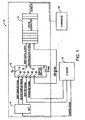
- Fig. 1 is a system having monitor circuitry configured to receive a first sampled signal and a second sampled signal from a device under test (DUT) for determining an operational status of the DUT.
- DUT device under test
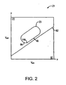
- Fig. 2 is a representation of an x-y plane showing a Lissajous figure in relation to a boundary, the boundary being indicative of a testing condition of the monitor circuitry of Fig. 1.
- Fig. 3 is a schematic diagram of the monitor circuitry of Fig. 1 in accordance with a first embodiment of the invention.
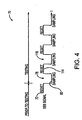
- Fig. 4 is a timing diagram illustrating an operational sequence of the monitor circuitry of Fig. 3.
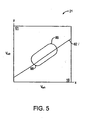
- Fig. 5 is a representation of the x-y plane of Fig. 2 indicating that the DUT may be defective when a coordinate of the Ussajous figure is in a particular zone.
- Fig. 6 is a representation of the x-y plane of Fig. 2 illustrating multiple different boundaries.
- Fig. 7 is a representation of an x-y plane having an unreachable zone in which a boundary may not be effectively established by the monitor circuitry of Fig. 3.
- Fig. 8 is a schematic diagram of the monitor circuitry of Fig. 1 in accordance with a second embodiment of the invention.
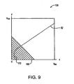
- Fig. 9 is a representation of an x-y plane having an unreachable zone in which a boundary may not be effectively established by the monitor circuitry of Fig. 8.
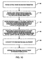
- Fig. 10 is a process flow diagram for identifying the test status of the DUT in accordance with the invention.
- Fig. 1 shows an on-chip system 10 in which monitor circuitry 12 is configured to receive a first sampled signal and a second sampled signal from a device under test (DUT) 14 in order to determine an operational status of the DUT.
- the DUT may be a mixed signal device or an analog device.
- the system also includes an IC tester 16, a digital compactor 18 and a comparator 120. While the comparator is shown as being off-chip (i.e., outside of the dashed lines), the comparator may also be on-chip.
- the monitor circuitry 12 is particularly suited for use as a built-in self-test (BIST) device in an on-chip environment.
- the monitor circuitry includes a first sampling terminal 20 and a second sampling terminal 22, a first reference terminal 24 and a second reference terminal 26, a first output terminal 28 and a second output terminal 30, a supply voltage (V DD ) input terminal 32, a sample and reset (SEB) terminal 34 and a ground terminal 36.
- V DD supply voltage
- SEB sample and reset
- the tester 16 is coupled to the DUT 14 to transmit a control signal.
- the control signal triggers transfers of first and second sampled signals from the DUT to the monitor circuitry 12.
- the first sampled signal is received by the monitor circuitry at the first sampling terminal 20.
- the second sampled signal is received by the monitor circuitry at the second sampling terminal 22.
- the sampled signals are analog signals and are indicative of two internal voltages within the DUT. Over a period of time, the sampled signals may define a Lissajous figure in an x-y plane. Using the x-y mode of an oscilloscope, the Lissajous figure may be visualized.
- Fig. 2 shows an x-y plane 21 having a Lissajous figure 23 that is characteristic of the DUT. For a DUT having linear characteristics, the Ussajous figure is likely to be elliptical.
- the first reference terminal 24 and the second reference terminal 26 are coupled to the tester 16 to receive a first reference signal and a second reference signal.
- the reference signals establish a testing condition within the monitor circuitry.
- the first and second reference signals are received from the DUT 14, rather than from the tester.
- the reference signals that are received from the DUT may be associated with reference points coupled to divider-based logic having discrete hard-wired voltage values.
- the SEB terminal 34 of the monitor circuitry 12 is connected to receive SEB signals from the tester 16 to trigger testing of the DUT 14. For each sampling time in a sequence of sampling times, a first digital output is generated at the first output terminal 28 and a second digital output is generated at the second output terminal 30. First and second digital outputs are continuously transferred to the digital compactor 18 for data compaction.
- Fig. 3 shows a schematic diagram of the monitor circuitry 12 of Fig. 1.
- the monitor circuitry includes a comparison circuit 40 (shown as a dashed block) and a sense amplifier 42 (also shown as a dashed block).
- the comparison circuit includes four transistors that are identified as transistors 44, 46, 48 and 50, but other embodiments may use a different number of transistors.
- the four transistors are cooperatively arranged in a parallel configuration.
- the four transistors may be conventional P-channel metal oxide semiconductor (PMOS) transistors.
- PMOS P-channel metal oxide semiconductor
- a supply voltage (V DD ) rail 52 is coupled to the supply voltage input terminal 32 of Fig. 1.
- a first switching transistor 54 is arranged between the V DD rail and the source regions (S) of the four transistors 44-50.
- the configuration of the first switching transistor is such that it can be selectively manipulated to either enable current to conduct through the four transistors or disable current from being conducted through the four transistors.
- the first switching transistor is an N-channel MOS (NMOS) transistor, but this is not critical.
- a first conduction path 56 for conducting a first current flow (I 1 ) is coupled to drain regions (D) of the transistors 44 and 46.
- a second conduction path 58 for conducting a second current flow (I 2 ) is coupled to drain regions (D) of the transistors 48 and 50.
- a second switching transistor 60 is coupled to the first conduction path and the second conduction path. The configuration of the second switching transistor is such that it can be selectively manipulated to provide a short-circuit condition or an open-circuit condition between the first conduction path and the second condition path.
- the second switching transistor may be an NMOS transistor.
- any two of the four transistors 44-50 may be selected to be control transistors or sense transistors.
- the transistor 46 is selected to be a first control transistor and the transistor 48 is selected to be a second control transistor.
- the first control transistor 46 is coupled to the first reference terminal 24 of Fig. 1 to receive the first reference signal at a gate region 62.
- the second control transistor 48 is coupled to the second reference terminal 26 of Fig. 1 to receive the second reference signal at a gate region 64.
- the remaining transistors 44 and 50 are first and second sense transistors.
- the first sense transistor 44 is coupled to the first sampling terminal 20 of Fig. 1 to receive the first sampled signal at a gate region 66.
- the second sense transistor 50 is coupled to the second sampling terminal 22 of Fig. 1 to receive the second sampled signal at a gate region 68.
- the operation of the comparison circuit 40 may be described with reference to the monitor circuitry 12 of Fig. 3 and the timing diagram 70 of Fig. 4.
- a high-level (i.e., logical high) SEB signal 72 is applied to the monitor circuitry to reset the comparison circuit.
- the high-level SEB signal is received at a gate region 74 of the first switching transistor 54 and at a gate region 76 of the second switching transistor 60.
- the first switching transistor and the second switching transistor are complementary switching transistors, such that the first switching transistor is activated when the second switching transistor is deactivated and the first switching transistor is deactivated when the second switching transistor is activated.
- the high-level SEB signal that is received at the gate region 74 of the first switching transistor deactivates the first switching transistor to establish an open-circuit condition between the V DD rail 52 and the four transistors 44-50. Accordingly, no current is conducted through any of the four transistors during the reset period.
- the high-level SEB signal that is received at the gate region 76 of the second switching transistor 60 activates the second switching transistor to establish a short-circuit condition between the first conduction path 56 and the second conduction path 58.
- the first current flow (I 1 ) at the first conduction path is equal to the second current flow (I 2 ) at the second conduction path.
- a low-level (logical low) SEB signal 80 is applied to the monitor circuitry 12 of Fig. 3.
- the low-level SEB signal is received at the gate region 74 of the first switching transistor 54 and at the gate region 76 of the second switching transistor 60.
- the low-level SEB signal that is received at the gate region 74 of the first switching transistor activates the first switching transistor to establish a substantially short-circuit condition between the V DD rail 52 and the four transistors 44-50. Accordingly, current flows are conducted through the four transistors 44-50, depending on the levels of voltages that are applied to the respective gate regions for controlling the levels of current through the transistors.
- the low-level SEB signal that is received at the gate region 76 of the second switching transistor 60 deactivates the second switching transistor to establish an open-circuit condition between the first conduction path 56 and the second conduction path 58.
- the first conduction path is electrically coupled to the first sense transistor 44 and the first control transistor 46.
- the second conduction path is electrically coupled to the second control transistor 48 and the second sense transistor 50. Accordingly, at the sampling instance, the first current flow (I 1 ) is dependent upon conduction through the first sense transistor and the first control transistor.
- the second current flow (I 2 ) is dependent upon conduction through the second control transistor and the second sense transistor.
- a testing condition that is characterized by a signal relationship between the first current flow (I 1 ) and the second current flow (I 2 ) is established by a specific level of current flow through the first control transistor 46 and a specific level of current flow through the second control transistor 48.
- the level of current flow through the first control transistor is regulated by the voltage level of the first reference signal received at the gate region 62.
- the level of current flow through the second control transistor is regulated by the voltage level of the second reference signal received at the gate region 64.
- the first and second reference signals are fixed voltages.
- a boundary 82 is indicative of the testing condition.
- the boundary is represented by a line that defines two identifiable zones.
- the zone that is on one side of the boundary may be identified as a zone 01 and the zone that is on the other side of the boundary may be identified as a zone 10 . While the boundary is represented by a line as shown in Fig. 2, the boundary may be a curve that can be created by changing the reference signals for each consecutive sampling instance.
- the level of current flow through the first sense transistor 44 is controlled by the voltage level of the first sampled signal at the gate region 66.
- the level of current flow through the second sense transistor 50 is controlled by the voltage level of the second sampled signal at the gate region 68.
- the first and second sampled signals define a coordinate 84 during the sampling instance.
- the coordinate is shown as being on the Lissajous figure 23, since the coordinate is identified during one sampling of the first and second sampled signals that form the Lissajous figure.
- the boundary 82 is shown as being at a distance 85 away from the Lissajous figure. The distance is indicative of a buffer zone to account for parametric variations exhibited by the DUT 14.
- the monitor circuitry 12 of Fig. 3 is designed to provide outputs that indicate whether the coordinate 84 lies in the zone 01 above the boundary 82 or in the zone 10 below the boundary.
- the testing condition set by the boundary may be one in which samples (Vref2) of the second sampled signal exceed simultaneously acquired samples (Vref1) by a factor of two.
- Vref2 samples of the second sampled signal exceed simultaneously acquired samples
- the outputs of the monitor circuitry will vary on the basis of the locations of coordinates defined by the samples acquired at the different sampling times, with each coordinate corresponding to a different sampling time.
- An output of the monitor circuitry indicates the relative position of a coordinate and the boundary by sensing the signal relationship of the first and second currents (I 1 and I 2 ).
- the signal relationship between the first current flow (I 1 ) and the second current flow (I 2 ) is varied when there is a change in the contribution from at least one of the first sense transistor 44 and the second sense transistor 50.
- the variation in the signal relationship indicates a location of the coordinate 84 with respect to the boundary 82 at the sampling instance.
- the variation indicates whether the coordinate is within the zone 01 because the first current flow is greater than the second current flow, or within the zone 10 , because the second current flow is greater than the first current flow.
- the variation in the signal relationship between the first current flow (I 1 ) and the second current flow (I 2 ) is indicative of the test status of the DUT 14.
- Fig. 2 shows the coordinate 84 as being located within the zone 01 at the first sampling instance 78 (Fig. 4).
- the variation in the signal relationship is subsequently digitized into a pair of digital outputs. At least one digital output from the pair of outputs is then compared with a corresponding digital reference signal obtained from a defect-free IC to determine the test status of the DUT. This is repeated for a sequence of output pairs.
- the status of the DUT 14 may be determined to be invalid if the signal relationship is one in which the second current flow is greater than the first current flow at the same first sampling instance 78 when the signal relationship of the defect-free IC is one in which the first current flow is greater than the second current flow.
- Fig. 5 shows the x-y plane 21 as having the same testing condition boundary 82 of Fig. 2.
- the x-y plane of Fig. 5 includes a Lissajous figure 86 of a defective DUT.
- the Lissajous figure 86 is at a different location from the Ussajous figure 23 of Fig. 2, since the Lissajous figure 86 is indicative of the defective DUT.
- a coordinate 88 is determined to be within the zone 10 , rather than within the zone 01 as would have been acquired from the defect-free IC.
- the different location of the coordinate is characterized by the signal relationship when the second current flow is greater than the first current flow. The signal relationship indicates that the DUT may be defective.
- the signal relationship between the first current flow (I 1 ) and the second current flow (I 2 ) is accelerated by the sense amplifier 42 of Fig. 3.
- the sense amplifier is coupled to the first and second conduction paths 56 and 58 from the comparison circuit 40.
- the sense amplifier includes a first accelerating transistor 90 and a second accelerating transistor 92, and a first enabling transistor 94 and a second enabling transistor 96.
- the first and second accelerating transistors may be PMOS transistors.
- the first and second enabling transistors may be NMOS transistors.
- the sense amplifier is configured to amplify a node voltage at a first node 98 when the first current flow is greater than the second current flow and to amplify a node voltage at a second node 100 when the second current flow is greater than the first current flow.
- the first node 98 is associated with the first conduction path 56, while the second node 100 is associated with the second conduction path 58.
- the operation of the sense amplifier 42 may be described with reference to the monitor circuitry 12 of Fig. 3 and the timing diagram 70 of Fig. 4.
- the high-level SEB signal 72 at the first switching transistor 54 and at the second switching transistor 60 is also received at the sense amplifier to reset the amplifier.
- the high-level SEB signal is coupled to a gate region 102 of the first enabling transistor 94 and a gate region 104 of the second enabling transistor 96.
- the high-level SEB signal at the gate region 102 activates the first enabling transistor to establish a short-circuit condition between the first conduction path 56 and electrical ground 105.
- the high-level SEB signal at the gate region 104 activates the second enabling transistor to establish a short-circuit condition between the second conduction path 58 and electrical ground. Accordingly, the first conduction path and the second conduction path are both shorted to ground in addition to being linked by the short-circuit condition that is established by the second switching transistor 60 during the reset period. Consequently, the first current flow is equal to the second current flow.
- the low-level SEB signal at the first switching transistor 54 and at the second switching transistor 60 is also received at the gate region 102 of the first enabling transistor 94 and at the gate region 104 of the second enabling transistor 96.
- the low-level SEB signal deactivates the first and second enabling transistors 94 and 96 to establish open-circuit conditions at the first and second enabling transistors. Accordingly, each of the first conduction path 56 and the second conduction path 58 is coupled to both the first and second accelerating transistors 90 and 92.
- the first and second accelerating transistors 90 and 92 are cooperatively configured to accelerate the variation in the signal relationship between the first current flow (I 1 ) and the second current flow (I 2 ) by amplifying a voltage differential between the first node 98 and the second node 100.
- the acceleration of the variation in the signal relationship will be described by way of an example in which the first current flow (I 1 ) is greater than the second current flow (I 2 ).
- the higher-level first current flow is reflected by a higher voltage level at the first node 98 and at a gate region 106 of the second accelerating transistor 92.
- the lower level of the second current flow is reflected by a lower voltage level at the second node 100 and at a gate region 108 of the first accelerating transistor 90.
- the higher voltage level at the gate region 106 activates the second accelerating transistor 92 to establish a conductive condition between the second node 100 and electrical ground 105. While the second accelerating transistor is activated, the second current flow is conducted to ground. Consequently, the node voltage at the second node is equalized to ground potential. As the second current flow is being conducted to ground, the voltage level at the gate region 108 of the first accelerating transistor 90 is further lowered due to lack of current contribution from the second current flow to the gate region of the first accelerating transistor. The drop in voltage at the gate region 108 deactivates the first accelerating transistor 90 to establish an open-circuit condition between the first node 98 and ground.
- the node voltage at the first node is equalized to the sum voltages of the first sense transistor 44 and the first control transistor 46. Since the node voltage at the second node 100 is equal to the ground potential, the node voltage at the first node 98 is amplified when compared to the node voltage at the second node.
- the monitor circuitry 12 also includes a first output inverter 110 and a second output inverter 112.
- the first output inverter is coupled to the first node 98 to invert the node voltage at the first node to a first digital output.
- the second output inverter 112 is coupled to the second node 100 to invert the node voltage at the second node to a second digital output.
- the first digital output and the second digital output are complementary digital outputs and are transmitted to the digital compactor 18 (Fig. 1) via respective first and second output terminals 28 and 30.
- the pair of the first and second digital outputs can be strobed at the same rate as the SEB signals.
- the digital compactor is configured to store multiple first and second digital outputs to generate a set of the first and second digital outputs.
- a high-level SEB signal 114 of Fig. 4 is applied to the monitor circuitry 12 of Fig. 3 to reset the circuitry for enabling a next sampling at a second sampling instance 116.
- a new pair of sampled signals is received at the comparison circuit 40.
- the new sampled signals vary the signal relationship between the first current flow (I 1 ) and the second current flow (I 2 ).
- the new sampled signals define a coordinate 118 within the x-y plane 21 of Fig. 2.
- the variation in the signal relationship indicates that the coordinate is within the zone 01 , because the first current flow is greater than the second current flow. The variation is accelerated by the sense amplifier.
- the monitor circuitry is configured to operate at a speed of 100 MHz. That is, the monitor circuitry can process 50 million samplings from the Lissajous figure within a one second interval.
- the set of first and second digital outputs is scanned-out of the digital compactor 18 to the comparator 120 of Fig. 1.
- the comparator is configured to compare the set of first and second digital outputs with a corresponding set of first and second predetermined digital reference signals to determine the operational status of the DUT.
- only the first or second digital output from the set of first and second digital outputs is compared with its corresponding first or second predetermined digital reference signal, since the first and second digital outputs are complementary digital outputs.
- the comparison sequence is tolerant to a finite range of mismatches before the DUT is declared as being faulty.
- the variation in the levels of current is attained by applying different constant voltages at the gate regions 62 and 64 of respective first and second control transistors 46 and 48.
- the variation establishes different x-y offsets, so that the slope of the boundary can be changed or the boundary can be moved upwardly or downwardly within the x-y plane.
- Fig. 6 shows a boundary 122 in the x-y plane 21 that is moved upwardly with respect to the boundary 82 of Fig. 2.
- the boundary 82 in Fig. 6 is shown as a dashed line to provide a perspective of the upward movement.
- the new boundary 122 defines two identifiable zones and enables multiple samplings of the Ussajous figure 23 (that is indicative of the DUT 14) to determine whether the Ussajous figure falls within one of the two identifiable zones. While the new boundary 122 is represented by a line as shown in Fig. 6, the new boundary may be a curve.
- the new boundary may be established by changing the connection order of the reference signals and the sampled signals with respect to the first conduction path 56 and the second conduction path 58 within the monitor circuitry 12 of Fig. 3. As shown in Fig. 6, the change in the connection order changes the slope of the boundary 82 to form a new boundary 124.
- the new boundary is established by selecting the transistors 44 and 46 to be respective first and second control transistors and the transistors 48 and 50 to be respective first and second sense transistors. This way, the first conduction path is coupled to two control transistors and the second conduction path is coupled to two sense transistors.
- the new boundary is established by selecting the transistors 44 and 46 to be respective first and second sense transistors and the transistors 48 and 50 to be respective first and second control transistors. Still, in another connection order, the new boundary is established by selecting the transistors 46 and 48 to be respective first and second sense transistors and the transistors 44 and 50 to be respective first and second control transistors.
- the changes to the connection orders may be performed by a switching multiplexer.
- the monitor circuitry may be adjusted multiple times in order to test the same sampling sequence for a variety of boundaries.
- the variety of boundaries may be established by an equal number of monitor circuits.
- the transistors 44-50 of the comparison circuit 40 of Fig. 3 are PMOS transistors. Due to the inherent limitations of the PMOS transistors, the performance of the comparison circuit is degraded when the voltage level that is applied to each of the four transistors 44-50 is near V DD . In such an event, there is an unreachable zone within the x-y plane where the boundary for defining the two zones cannot be effectively established. Consequently, the locations of coordinates that are indicative of a Ussajous figure may not be properly identified as being within one of the two predetermined zones, if the Lissajous figure also falls within the unreachable zone. Fig.
- the unreachable zone 126 (indicated by cross-hatching) in an x-y plane 128.
- the unreachable zone includes a non-linear portion 129 (shown in dash) of the boundary 82. Around the non-linear portion, the boundary for establishing the two zones cannot be effectively established.
- FIG. 8 shows a schematic diagram of a monitor circuitry 130 in accordance with a second embodiment of the invention.
- the monitor circuitry 130 includes a comparison circuit 132 and a sense amplifier 134.
- the comparison circuit includes four transistors that are identified as NMOS transistors 136, 138, 140 and 142.
- the sense amplifier includes a first accelerating transistor 144 and a second accelerating transistor 146 that are NMOS transistors, and a first enabling transistor 148 and a second enabling transistor 150 that are PMOS transistors.
- any two of the four transistors 136-142 of the comparison circuit 132 of Fig. 8 may be selected to be control transistors or sense transistors.
- the transistor 138 is selected to be the first control transistor and the transistor 140 is selected to be the second control transistor.
- the transistor 136 is the first sense transistor and the transistor 142 is the second sense transistor.
- a first conduction path 152 for a first current flow (I 1 ) and a second conduction path 154 for a second current flow (I 2 ) are coupled between the comparison circuit 132 and the sense amplifier 134.
- the first conduction path 152 is coupled to the comparison circuit at drain regions (D) of the first sense transistor 136 and the first control transistor 138.
- the second conduction path 154 is coupled to the comparison circuit at drain regions (D) of the second control transistor 140 and the second sense transistor 142.
- a high-level SEB signal is received at a first switching transistor 156 and at a second switching transistor 158.
- the high-level SEB signal at the first switching transistor activates the first switching transistor to establish a short-circuit condition between the source regions of the four transistors 136-142 and ground to enable currents to flow from a V DD rail 160 to ground.
- the high-level SEB signal that is received at the second switching transistor 158 deactivates the second switching transistor to establish an open-circuit condition.
- the first conduction path 152 is electrically coupled to the first sense transistor 136 and the first control transistor 138.
- the second conduction path 154 is electrically coupled to the second control transistor 140 and the second sense transistor 142.
- a testing condition that is characterized by a signal relationship between the first current flow (I 1 ) through the first conduction path 152 and the second current flow (I 2 ) through the second conduction path 154 is established by a specific level of current flow through the first control transistor 138 and a specific level of current flow through the second control transistor 140.
- the testing condition may be represented by the boundary 82 within the x-y plane 21 of Fig. 2. As described earlier, the boundary defines two identifiable zones (e.g., zone 01 and zone 10 ) within the x-y plane.
- the signal relationship is considered when samples are applied to the first sense transistor 136 and the second sense transistor 142.
- the current flow through the first sense transistor is controlled by the first sampled signal at a gate region of the first sense transistor.
- the current flow through the second sense transistor is controlled by the second sampled signal at a gate region of the second sense transistor.
- the first and second sampled signals define the coordinate 84 within the x-y plane 21.
- the variation in the signal relationship indicates the location of the coordinate with respect to the boundary 82. In one testing scenario, the variation indicates whether the coordinate is on one side of the boundary within the zone 01 , because the first current flow is greater than the second current flow, or is on the other side of the boundary within the zone 10 , because the second current flow is greater than the first current flow.
- the signal relationship between the first current flow (I 1 ) and the second current flow (I 2 ) is accelerated by the sense amplifier 134 of Fig. 8.
- the sense amplifier is coupled to the first and second conduction paths 152 and 154. Similar to the sense amplifier 42 of Fig. 3, the sense amplifier 134 is configured to amplify a node voltage at a first node 162 when the first current flow is greater than the second current flow and to amplify a node voltage at a second node 164 when the second current flow is greater than the first current flow.
- a first output inverter 166 is coupled to the first node 162 to invert the node voltage at the first node to generate a first digital output.
- a second output inverter 168 is coupled to the second node 164 to invert the node voltage at the second node to generate a second digital output.
- the first digital output and the second digital output are complementary digital outputs that are transmitted to the digital compactor 18 of Fig. 1.
- the comparison circuit 132 of Fig. 8 can effectively establish a boundary for defining two identifiable zones when the voltages that are applied to each of the four transistors 136-142 is near V DD , the performance of the comparison circuit is degraded when the voltages are near zero. The degradation in performance is due to the inherent limitations of the NMOS transistors 136-142. When the voltage level is near zero, there is an unreachable zone within the x-y plane where the boundary for defining the two zones cannot be effectively established. Consequently, the locations of coordinates that are indicative of a Lissajous figure may not be property identified as being within one of the two pre-determined zones, if the Ussajous figure also falls within the unreachable zone. Fig.
- the unreachable zone 169 shows an unreachable zone 169 (indicated by cross-hatching) in the x-y plane 128.
- the unreachable zone includes a non-linear portion 170 (shown in dash) of the boundary 82. Around the non-linear portion, the boundary for establishing the two zones cannot be effectively established. However, the problem associated with properly defining the boundary within the unreachable zone is solved by the use of PMOS transistors within the comparison circuit 40 of Fig. 3.
- step 180 control transistors and sense transistors are provided. As shown by the monitor circuitry 12 of Fig. 3, there are two control transistors and two sense transistors. The four transistors are arranged in parallel. In the monitor circuitry, the transistor 46 is the first control transistor and the transistor 48 is the second control transistor. The transistor 44 is the first sense transistor and the transistor 50 is the second sense transistor.
- a first current path (I 1 ) for conducting a first current flow is provided.
- a second current path (I 2 ) for conducting a second current flow is also provided.
- the step of providing the first current path and the second current path includes connecting the first current path to source/drain regions of any two of the four transistors and connecting the second current path to source/drain regions of the other two transistors.
- the first conduction path 56 is coupled to the drain regions of the first sense transistor 44 and the first control transistor 46.
- the second conduction path 58 is coupled to the drain regions of the second control transistor 48 and the second sense transistor 50.
- step 184 reference signals are received at the control transistors to establish a testing condition with respect to a signal relationship between the first current flow and the second current flow.
- the reference signals are constant levels of voltages for controlling the current flows that are conducted through the control transistors.
- the reference signals may define a number of regions in an x-y plane, including the zone 01 and the zone 10 within the x-y plane 21 of Fig. 2.
- sampled signals are received from the DUT.
- the sampled signals are analog signals which are applied to control the current flows through the sense transistors.
- the sampled signals define a coordinate, such as the coordinate 84 that is shown within the x-y plane 21 of Fig. 2.
- the sampled signals vary the signal relationship between the first current flow and the second current flow.
- the resulting signal relationship indicates the region in which the sampled coordinate resides.
- the coordinate 84 is identified as being located within the zone 01 when the signal relationship is such that the first current flow is greater than the second current flow.
- step 188 the variation in the signal relationship is accelerated by a sense amplifier, such as the sense amplifier 42 of Fig. 3.
- a sense amplifier such as the sense amplifier 42 of Fig. 3.
- the status of the DUT is determined in step 190 on the basis of the digital outputs from the monitor circuitry.
Landscapes
- Engineering & Computer Science (AREA)
- General Engineering & Computer Science (AREA)
- Physics & Mathematics (AREA)
- General Physics & Mathematics (AREA)
- Tests Of Electronic Circuits (AREA)
Description
- The invention relates generally to the testing of integrated circuits (ICs) and more particularly to monitor circuitry and a method for testing analog and/or mixed signal ICs.
- Continuing increases in the complexity and density of analog and mixed signal integrated circuits (ICs) have imposed a challenge to the testing of circuitry within the circuits. A specific circuit design may exhibit a particular "signature" with respect to signal responses. While signature analysis has been successfully used to detect faults within digital ICs, the use of signature analysis for detecting faults within analog and mixed signal ICs is still in its infancy.
- In current analog and mixed signal ICs testing techniques, the analog signals for testing are often distorted due to the need to transfer the signals to an off-chip environment. Test buses (e.g., IEEE 1149.4 standard), scan circuitry, oscilloscopes, and signal processing algorithms are often required, thereby adding to the problems encountered with parasitic loading and coupling.
- One approach for testing analog and mixed signal ICs without the need to transfer the signals to the off-chip environment is to implement a built-in self-test (BIST) scheme. Since the analyses are performed on-chip, many of the problems associated with off-chip testings are eliminated. Brosa and Figueras in Digital Signature Proposal for Mixed-Signal Circuits, ITC International Test Conference, IEEE (2000), describe a system and method for testing mixed-signal ICs using a BIST scheme. According to the system, a zone detector is used to generate a control line that is swept across a Lissajous figure which is signatory of the IC. At each predefined period, a zero-crossing detector and counter counts the number of times the control line crosses the Lissajous figure. The number of crossings in the predefined period indicates the operational status of the IC. The zone detector for generating the control line consists of three operational amplifiers (op-amps) that are arranged in successive stages. One concern with the use of op-amps is the excessive area requirements of the op-amps, as compared to the IC under test, since each op-amp requires a significant amount of circuitry for implementation. Another concern is that the circuitry within the op-amps adds to the complexity and cost of manufacturing.
- While the publication does not describe a system or method for testing integrated circuits, a circuit which may be used in a current mode analog-to-digital converter is described by Lahiji et al. in the reference entitled "A Full Differential Low Voltage Low Power High Speed Current Comparator," in Microelectronics, 2000, ICM 2000 Proceedings of the 12th International Conference on October 31-November 2, 2002 (Piscataway, NJ, USA, IEEE, 31 October 2000, pages 103-106, ISBN:964-360-057-2). The circuit includes a pair of latch transistors (M1 and M2) and a pair of switching transistors (M7 and M8) which define a first mode and a second mode of operation. In the first mode, one switching transistor is turned on and the other is turned off and the output node voltages are connected together.
- However, due to the presence of an input differential current, there is still a small difference in the node voltages. During the second mode, by changing the states of the two switching transistors, the small difference in the node voltage is amplified to a state in which one branch is high and the other is low, with the resulting states being saved in two flip-flops. In order to bias the latch transistors (M1 and M2) during the first mode of operation, transistor pair (M5 and M6) is added. The bias current of these transistors must be kept as low as possible in order to reduce power dissipation. Finally, a transistor pair (M3 and M4) is added to enhance the speed of regeneration in the latch by injecting a higher amount of current.
- What is needed is a system and method for testing analog and mixed signal ICs, such that the size, complexity, and cost of manufacturing are reduced.
- Monitor circuitry for identifying an operational status of a device under test (DUT) includes a comparison circuit and a sense amplifier. The comparison circuit comprises a set of control transistors and a set of sense transistors. The control transistors include control input terminals for receiving reference signals. The reference signals establish a testing condition that is characterized by a signal relationship between a first current flow and a second current flow. The sense transistors are operatively associated with the control transistors, such that biasing sense input terminals of the sense transistors with sampled signals received from the DUT varies the signal relationship between the first current flow and the second current flow. The variation in the signal relationship is accelerated by the sense amplifier. The variation in the signal relationship is indicative of the operational status of the DUT at the sampling instance of acquiring the sampled signals.
- In one embodiment, the comparison circuit includes four transistors that are cooperatively arranged in a parallel configuration, including two control transistors and two sense transistors. A first conduction path for the first current flow is coupled to the source/drain regions of two of the four transistors. A second conduction path for the second current flow is coupled to the source/drain regions of the other two transistors. The first and second conduction paths are in parallel from the four transistors of the parallel configuration to the sense amplifier.
- The parallel configuration may be arranged such that: (1) the two control transistors are connected to the first conduction path and the two sense transistors are connected to the second conduction path, (2) the two control transistors are connected to the second conduction path and the two sense transistors are connected to the first conduction path, and (3) one control transistor and one sense transistor are connected to the first conduction path while the other control transistor and the other sense transistor are connected to the second conduction path. Accordingly, each of the conduction paths may be coupled to the source/drain regions of: (1) two control transistors, (2) two sense transistors, or (3) one control transistor and one sense transistor.
- Prior to testing, the monitor circuitry is initialized such that the first current flow at the first conduction path is equal to the second current flow at the second conduction path, if the two sampled signals satisfy a specific signal relationship condition. At a sampling instance, a set of reference signals is received at the control input terminals of the two control transistors. The reference signals may be constant voltages for controlling the current flows that are conducted through the two control transistors. The reference signals establish a testing condition with respect to the signal relationship between the first current flow and the second current flow. In an x-y plane, the reference signals are indicative of a boundary that divides two identifiable zones.
- At a testing instance, a set of sampled signals are received at the sense input terminals of the two sense transistors. The sampled signals are analog signals which will determine the current flows that are conducted through the two sense transistors. The sampled signals vary the signal relationship between the first current flow and the second current flow. In the x-y plane, the sampled signals define a coordinate. The variation in the signal relationship indicates a location of the coordinate with respect to the boundary. In one testing scenario, the variation indicates whether the coordinate is on one side of the boundary because the first current flow is greater than the second current flow or on the other side of the boundary because the second current flow is greater than the first current flow.
- The changes in the signal relationship between the first current flow and the second current flow are accelerated by the sense amplifier. The sense amplifier is configured to amplify a node voltage at a first node when the first current flow is greater than the second current flow or to amplify a node voltage at a second node when the second current flow is greater than the first current flow.
- The monitor circuitry may also include output inverters. A first output inverter is coupled to the first node to invert the node voltage at the first node to provide a first digital output. A second output inverter is coupled to the second node to invert the node voltage at the second node to provide a second digital output. The first digital output and the second digital output are complementary digital outputs.
- In accordance with the inventive method, a sequence of first and second digital outputs is generated using sequential sampled signals. Moreover, the reference signals may be adjusted to define other boundaries in the x-y plane. Subsequent downstream processing compares at least one of the first and second digital outputs with a corresponding predetermined reference digital signal to determine the operational status of the DUT.
- An advantage of the invention is that the operational status of the DUT can be determined by a relatively simple device. This is potentially important, since the simplicity of the device reduces the hardware requirements needed for testing. Accordingly, the test status of the DUT is determined in a relatively short period of time. Moreover, the cost overhead for manufacturing is significantly reduced relative to the prior art.
- Fig. 1 is a system having monitor circuitry configured to receive a first sampled signal and a second sampled signal from a device under test (DUT) for determining an operational status of the DUT.
- Fig. 2 is a representation of an x-y plane showing a Lissajous figure in relation to a boundary, the boundary being indicative of a testing condition of the monitor circuitry of Fig. 1.
- Fig. 3 is a schematic diagram of the monitor circuitry of Fig. 1 in accordance with a first embodiment of the invention.
- Fig. 4 is a timing diagram illustrating an operational sequence of the monitor circuitry of Fig. 3.
- Fig. 5 is a representation of the x-y plane of Fig. 2 indicating that the DUT may be defective when a coordinate of the Ussajous figure is in a particular zone.
- Fig. 6 is a representation of the x-y plane of Fig. 2 illustrating multiple different boundaries.
- Fig. 7 is a representation of an x-y plane having an unreachable zone in which a boundary may not be effectively established by the monitor circuitry of Fig. 3.
- Fig. 8 is a schematic diagram of the monitor circuitry of Fig. 1 in accordance with a second embodiment of the invention.
- Fig. 9 is a representation of an x-y plane having an unreachable zone in which a boundary may not be effectively established by the monitor circuitry of Fig. 8.
- Fig. 10 is a process flow diagram for identifying the test status of the DUT in accordance with the invention.
- Fig. 1 shows an on-
chip system 10 in which monitorcircuitry 12 is configured to receive a first sampled signal and a second sampled signal from a device under test (DUT) 14 in order to determine an operational status of the DUT. The DUT may be a mixed signal device or an analog device.
The system also includes anIC tester 16, adigital compactor 18 and acomparator 120. While the comparator is shown as being off-chip (i.e., outside of the dashed lines), the comparator may also be on-chip. - The
monitor circuitry 12 is particularly suited for use as a built-in self-test (BIST) device in an on-chip environment. The monitor circuitry includes afirst sampling terminal 20 and asecond sampling terminal 22, afirst reference terminal 24 and asecond reference terminal 26, afirst output terminal 28 and asecond output terminal 30, a supply voltage (VDD)input terminal 32, a sample and reset (SEB)terminal 34 and aground terminal 36. - The
tester 16 is coupled to theDUT 14 to transmit a control signal. The control signal triggers transfers of first and second sampled signals from the DUT to themonitor circuitry 12. The first sampled signal is received by the monitor circuitry at thefirst sampling terminal 20. The second sampled signal is received by the monitor circuitry at thesecond sampling terminal 22. The sampled signals are analog signals and are indicative of two internal voltages within the DUT. Over a period of time, the sampled signals may define a Lissajous figure in an x-y plane. Using the x-y mode of an oscilloscope, the Lissajous figure may be visualized. Fig. 2 shows anx-y plane 21 having a Lissajous figure 23 that is characteristic of the DUT. For a DUT having linear characteristics, the Ussajous figure is likely to be elliptical. - In the
monitor circuitry 12 of Fig. 1, thefirst reference terminal 24 and thesecond reference terminal 26 are coupled to thetester 16 to receive a first reference signal and a second reference signal. As will be explained in detail below, the reference signals establish a testing condition within the monitor circuitry. In a different embodiment, the first and second reference signals are received from theDUT 14, rather than from the tester. The reference signals that are received from the DUT may be associated with reference points coupled to divider-based logic having discrete hard-wired voltage values. - The
SEB terminal 34 of themonitor circuitry 12 is connected to receive SEB signals from thetester 16 to trigger testing of theDUT 14. For each sampling time in a sequence of sampling times, a first digital output is generated at thefirst output terminal 28 and a second digital output is generated at thesecond output terminal 30. First and second digital outputs are continuously transferred to thedigital compactor 18 for data compaction. - In accordance with a first embodiment of the invention, Fig. 3 shows a schematic diagram of the
monitor circuitry 12 of Fig. 1. The monitor circuitry includes a comparison circuit 40 (shown as a dashed block) and a sense amplifier 42 (also shown as a dashed block). In the embodiment of Fig. 3, the comparison circuit includes four transistors that are identified astransistors - A supply voltage (VDD)
rail 52 is coupled to the supplyvoltage input terminal 32 of Fig. 1. Afirst switching transistor 54 is arranged between the VDD rail and the source regions (S) of the four transistors 44-50. The configuration of the first switching transistor is such that it can be selectively manipulated to either enable current to conduct through the four transistors or disable current from being conducted through the four transistors. The first switching transistor is an N-channel MOS (NMOS) transistor, but this is not critical. - A
first conduction path 56 for conducting a first current flow (I1) is coupled to drain regions (D) of thetransistors second conduction path 58 for conducting a second current flow (I2) is coupled to drain regions (D) of thetransistors second switching transistor 60 is coupled to the first conduction path and the second conduction path. The configuration of the second switching transistor is such that it can be selectively manipulated to provide a short-circuit condition or an open-circuit condition between the first conduction path and the second condition path. The second switching transistor may be an NMOS transistor. - Within the
comparison circuit 40, any two of the four transistors 44-50 may be selected to be control transistors or sense transistors. In one exemplary embodiment, thetransistor 46 is selected to be a first control transistor and thetransistor 48 is selected to be a second control transistor. Thefirst control transistor 46 is coupled to thefirst reference terminal 24 of Fig. 1 to receive the first reference signal at a gate region 62. Thesecond control transistor 48 is coupled to thesecond reference terminal 26 of Fig. 1 to receive the second reference signal at a gate region 64. In the same exemplary embodiment, the remainingtransistors first sense transistor 44 is coupled to thefirst sampling terminal 20 of Fig. 1 to receive the first sampled signal at agate region 66. Thesecond sense transistor 50 is coupled to thesecond sampling terminal 22 of Fig. 1 to receive the second sampled signal at agate region 68. - The operation of the
comparison circuit 40 may be described with reference to themonitor circuitry 12 of Fig. 3 and the timing diagram 70 of Fig. 4. Prior to testing, a high-level (i.e., logical high)SEB signal 72 is applied to the monitor circuitry to reset the comparison circuit. The high-level SEB signal is received at agate region 74 of thefirst switching transistor 54 and at agate region 76 of thesecond switching transistor 60. The first switching transistor and the second switching transistor are complementary switching transistors, such that the first switching transistor is activated when the second switching transistor is deactivated and the first switching transistor is deactivated when the second switching transistor is activated. The high-level SEB signal that is received at thegate region 74 of the first switching transistor deactivates the first switching transistor to establish an open-circuit condition between the VDD rail 52 and the four transistors 44-50. Accordingly, no current is conducted through any of the four transistors during the reset period. The high-level SEB signal that is received at thegate region 76 of thesecond switching transistor 60 activates the second switching transistor to establish a short-circuit condition between thefirst conduction path 56 and thesecond conduction path 58. During the short-circuit condition, the first current flow (I1) at the first conduction path is equal to the second current flow (I2) at the second conduction path. - At a
first sampling instance 78 of Fig. 4, a low-level (logical low)SEB signal 80 is applied to themonitor circuitry 12 of Fig. 3. The low-level SEB signal is received at thegate region 74 of thefirst switching transistor 54 and at thegate region 76 of thesecond switching transistor 60. The low-level SEB signal that is received at thegate region 74 of the first switching transistor activates the first switching transistor to establish a substantially short-circuit condition between the VDD rail 52 and the four transistors 44-50. Accordingly, current flows are conducted through the four transistors 44-50, depending on the levels of voltages that are applied to the respective gate regions for controlling the levels of current through the transistors. The low-level SEB signal that is received at thegate region 76 of thesecond switching transistor 60 deactivates the second switching transistor to establish an open-circuit condition between thefirst conduction path 56 and thesecond conduction path 58. During the open-circuit condition, the first conduction path is electrically coupled to thefirst sense transistor 44 and thefirst control transistor 46. The second conduction path is electrically coupled to thesecond control transistor 48 and thesecond sense transistor 50. Accordingly, at the sampling instance, the first current flow (I1) is dependent upon conduction through the first sense transistor and the first control transistor. The second current flow (I2) is dependent upon conduction through the second control transistor and the second sense transistor. - A testing condition that is characterized by a signal relationship between the first current flow (I1) and the second current flow (I2) is established by a specific level of current flow through the
first control transistor 46 and a specific level of current flow through thesecond control transistor 48. The level of current flow through the first control transistor is regulated by the voltage level of the first reference signal received at the gate region 62. The level of current flow through the second control transistor is regulated by the voltage level of the second reference signal received at the gate region 64. The first and second reference signals are fixed voltages. In thex-y plane 21 of Fig. 2, aboundary 82 is indicative of the testing condition. The boundary is represented by a line that defines two identifiable zones. The zone that is on one side of the boundary may be identified as azone 01 and the zone that is on the other side of the boundary may be identified as azone 10. While the boundary is represented by a line as shown in Fig. 2, the boundary may be a curve that can be created by changing the reference signals for each consecutive sampling instance. - At the same first sampling instance 78 (Fig. 4), the level of current flow through the
first sense transistor 44 is controlled by the voltage level of the first sampled signal at thegate region 66. The level of current flow through thesecond sense transistor 50 is controlled by the voltage level of the second sampled signal at thegate region 68. In thex-y plane 21 of Fig. 2, the first and second sampled signals define a coordinate 84 during the sampling instance. The coordinate is shown as being on the Lissajous figure 23, since the coordinate is identified during one sampling of the first and second sampled signals that form the Lissajous figure. Theboundary 82 is shown as being at adistance 85 away from the Lissajous figure. The distance is indicative of a buffer zone to account for parametric variations exhibited by theDUT 14. - The
monitor circuitry 12 of Fig. 3 is designed to provide outputs that indicate whether the coordinate 84 lies in thezone 01 above theboundary 82 or in thezone 10 below the boundary. Merely as an example, the testing condition set by the boundary may be one in which samples (Vref2) of the second sampled signal exceed simultaneously acquired samples (Vref1) by a factor of two. For a set testing condition, the outputs of the monitor circuitry will vary on the basis of the locations of coordinates defined by the samples acquired at the different sampling times, with each coordinate corresponding to a different sampling time. An output of the monitor circuitry indicates the relative position of a coordinate and the boundary by sensing the signal relationship of the first and second currents (I1 and I2). - The signal relationship between the first current flow (I1) and the second current flow (I2) is varied when there is a change in the contribution from at least one of the
first sense transistor 44 and thesecond sense transistor 50. In thex-y plane 21 of Fig. 2, the variation in the signal relationship indicates a location of the coordinate 84 with respect to theboundary 82 at the sampling instance. In one testing scenario, the variation indicates whether the coordinate is within thezone 01 because the first current flow is greater than the second current flow, or within thezone 10, because the second current flow is greater than the first current flow. - The variation in the signal relationship between the first current flow (I1) and the second current flow (I2) is indicative of the test status of the
DUT 14. As an example, Fig. 2 shows the coordinate 84 as being located within thezone 01 at the first sampling instance 78 (Fig. 4). As will be explained in detail below, the variation in the signal relationship is subsequently digitized into a pair of digital outputs. At least one digital output from the pair of outputs is then compared with a corresponding digital reference signal obtained from a defect-free IC to determine the test status of the DUT. This is repeated for a sequence of output pairs. - The status of the
DUT 14 may be determined to be invalid if the signal relationship is one in which the second current flow is greater than the first current flow at the samefirst sampling instance 78 when the signal relationship of the defect-free IC is one in which the first current flow is greater than the second current flow. As an example, Fig. 5 shows thex-y plane 21 as having the sametesting condition boundary 82 of Fig. 2. The x-y plane of Fig. 5 includes a Lissajous figure 86 of a defective DUT. The Lissajous figure 86 is at a different location from the Ussajous figure 23 of Fig. 2, since the Lissajous figure 86 is indicative of the defective DUT. At the same first sampling instance, a coordinate 88 is determined to be within thezone 10, rather than within thezone 01 as would have been acquired from the defect-free IC. The different location of the coordinate is characterized by the signal relationship when the second current flow is greater than the first current flow. The signal relationship indicates that the DUT may be defective. - The signal relationship between the first current flow (I1) and the second current flow (I2) is accelerated by the
sense amplifier 42 of Fig. 3. The sense amplifier is coupled to the first andsecond conduction paths comparison circuit 40. The sense amplifier includes a first acceleratingtransistor 90 and a second acceleratingtransistor 92, and a first enablingtransistor 94 and a second enablingtransistor 96. The first and second accelerating transistors may be PMOS transistors. The first and second enabling transistors may be NMOS transistors. The sense amplifier is configured to amplify a node voltage at afirst node 98 when the first current flow is greater than the second current flow and to amplify a node voltage at a second node 100 when the second current flow is greater than the first current flow. Thefirst node 98 is associated with thefirst conduction path 56, while the second node 100 is associated with thesecond conduction path 58. - The operation of the
sense amplifier 42 may be described with reference to themonitor circuitry 12 of Fig. 3 and the timing diagram 70 of Fig. 4. Prior to testing, the high-level SEB signal 72 at thefirst switching transistor 54 and at thesecond switching transistor 60 is also received at the sense amplifier to reset the amplifier. The high-level SEB signal is coupled to agate region 102 of the first enablingtransistor 94 and agate region 104 of the second enablingtransistor 96. The high-level SEB signal at thegate region 102 activates the first enabling transistor to establish a short-circuit condition between thefirst conduction path 56 andelectrical ground 105. Similarly, the high-level SEB signal at thegate region 104 activates the second enabling transistor to establish a short-circuit condition between thesecond conduction path 58 and electrical ground. Accordingly, the first conduction path and the second conduction path are both shorted to ground in addition to being linked by the short-circuit condition that is established by thesecond switching transistor 60 during the reset period. Consequently, the first current flow is equal to the second current flow. - At the
first sampling instance 78 of Fig. 4, the low-level SEB signal at thefirst switching transistor 54 and at thesecond switching transistor 60 is also received at thegate region 102 of the first enablingtransistor 94 and at thegate region 104 of the second enablingtransistor 96. The low-level SEB signal deactivates the first and second enablingtransistors first conduction path 56 and thesecond conduction path 58 is coupled to both the first and second acceleratingtransistors - The first and second accelerating
transistors first node 98 and the second node 100. The acceleration of the variation in the signal relationship will be described by way of an example in which the first current flow (I1) is greater than the second current flow (I2). The higher-level first current flow is reflected by a higher voltage level at thefirst node 98 and at agate region 106 of the second acceleratingtransistor 92. The lower level of the second current flow is reflected by a lower voltage level at the second node 100 and at agate region 108 of the first acceleratingtransistor 90. The higher voltage level at thegate region 106 activates the second acceleratingtransistor 92 to establish a conductive condition between the second node 100 andelectrical ground 105. While the second accelerating transistor is activated, the second current flow is conducted to ground. Consequently, the node voltage at the second node is equalized to ground potential. As the second current flow is being conducted to ground, the voltage level at thegate region 108 of the first acceleratingtransistor 90 is further lowered due to lack of current contribution from the second current flow to the gate region of the first accelerating transistor. The drop in voltage at thegate region 108 deactivates the first acceleratingtransistor 90 to establish an open-circuit condition between thefirst node 98 and ground. With the first accelerating transistor being in the open-circuit condition, the node voltage at the first node is equalized to the sum voltages of thefirst sense transistor 44 and thefirst control transistor 46. Since the node voltage at the second node 100 is equal to the ground potential, the node voltage at thefirst node 98 is amplified when compared to the node voltage at the second node. - The
monitor circuitry 12 also includes afirst output inverter 110 and asecond output inverter 112. The first output inverter is coupled to thefirst node 98 to invert the node voltage at the first node to a first digital output. Thesecond output inverter 112 is coupled to the second node 100 to invert the node voltage at the second node to a second digital output The first digital output and the second digital output are complementary digital outputs and are transmitted to the digital compactor 18 (Fig. 1) via respective first andsecond output terminals - Subsequent to generating the first and second digital outputs, a high-level SEB signal 114 of Fig. 4 is applied to the
monitor circuitry 12 of Fig. 3 to reset the circuitry for enabling a next sampling at asecond sampling instance 116. At the second sampling instance, a new pair of sampled signals is received at thecomparison circuit 40. The new sampled signals vary the signal relationship between the first current flow (I1) and the second current flow (I2). In one exemplary embodiment, the new sampled signals define a coordinate 118 within thex-y plane 21 of Fig. 2. The variation in the signal relationship indicates that the coordinate is within thezone 01, because the first current flow is greater than the second current flow. The variation is accelerated by the sense amplifier. A new pair of digital outputs is generated and transmitted to thedigital compactor 18. Subsequently, the testing sequence is repeated with another pair of sampled signals to generate first and second digital outputs. In one embodiment, the monitor circuitry is configured to operate at a speed of 100 MHz. That is, the monitor circuitry can process 50 million samplings from the Lissajous figure within a one second interval. - When a threshold number of the first and second digital outputs is reached, the set of first and second digital outputs is scanned-out of the
digital compactor 18 to thecomparator 120 of Fig. 1. In one embodiment, the comparator is configured to compare the set of first and second digital outputs with a corresponding set of first and second predetermined digital reference signals to determine the operational status of the DUT. In another embodiment, only the first or second digital output from the set of first and second digital outputs is compared with its corresponding first or second predetermined digital reference signal, since the first and second digital outputs are complementary digital outputs. As indicated earlier, if the signal relationship for a defective DUT is such that the second current flow is greater than the first current flow, the "incorrect" signal relationship will be indicated by the digital outputs. When the digital outputs are compared to the predetermined digital reference signals, the mismatch will be noted. In one embodiment, the comparison sequence is tolerant to a finite range of mismatches before the DUT is declared as being faulty. - Specific levels of current flow through the first and
second control transistors monitor circuitry 12 of Fig. 3 establish theboundary 82 of Fig. 2 for defining the testing condition, but a different boundary may be established to define a new testing condition by varying the levels of current through the first andsecond control transistors second control transistors boundary 122 in thex-y plane 21 that is moved upwardly with respect to theboundary 82 of Fig. 2. Theboundary 82 in Fig. 6 is shown as a dashed line to provide a perspective of the upward movement. Thenew boundary 122 defines two identifiable zones and enables multiple samplings of the Ussajous figure 23 (that is indicative of the DUT 14) to determine whether the Ussajous figure falls within one of the two identifiable zones. While thenew boundary 122 is represented by a line as shown in Fig. 6, the new boundary may be a curve. - In another embodiment, the new boundary may be established by changing the connection order of the reference signals and the sampled signals with respect to the
first conduction path 56 and thesecond conduction path 58 within themonitor circuitry 12 of Fig. 3. As shown in Fig. 6, the change in the connection order changes the slope of theboundary 82 to form anew boundary 124. In one connection order, the new boundary is established by selecting thetransistors transistors transistors transistors transistors transistors - The monitor circuitry may be adjusted multiple times in order to test the same sampling sequence for a variety of boundaries. As an alternative, the variety of boundaries may be established by an equal number of monitor circuits.
- As indicated earlier, the transistors 44-50 of the
comparison circuit 40 of Fig. 3 are PMOS transistors. Due to the inherent limitations of the PMOS transistors, the performance of the comparison circuit is degraded when the voltage level that is applied to each of the four transistors 44-50 is near VDD. In such an event, there is an unreachable zone within the x-y plane where the boundary for defining the two zones cannot be effectively established. Consequently, the locations of coordinates that are indicative of a Ussajous figure may not be properly identified as being within one of the two predetermined zones, if the Lissajous figure also falls within the unreachable zone. Fig. 7 shows an unreachable zone 126 (indicated by cross-hatching) in anx-y plane 128. The unreachable zone includes a non-linear portion 129 (shown in dash) of theboundary 82. Around the non-linear portion, the boundary for establishing the two zones cannot be effectively established. - The problem associated with properly defining a boundary within the unreachable zone is solved by a comparison circuit that uses NMOS transistors. Fig. 8 shows a schematic diagram of a
monitor circuitry 130 in accordance with a second embodiment of the invention. Themonitor circuitry 130 includes acomparison circuit 132 and asense amplifier 134. The comparison circuit includes four transistors that are identified asNMOS transistors transistor 144 and a second acceleratingtransistor 146 that are NMOS transistors, and a first enablingtransistor 148 and a second enablingtransistor 150 that are PMOS transistors. - Similar to the
comparison circuit 40 of Fig. 3, any two of the four transistors 136-142 of thecomparison circuit 132 of Fig. 8 may be selected to be control transistors or sense transistors. In one exemplary embodiment, thetransistor 138 is selected to be the first control transistor and thetransistor 140 is selected to be the second control transistor. Thetransistor 136 is the first sense transistor and thetransistor 142 is the second sense transistor. Afirst conduction path 152 for a first current flow (I1) and asecond conduction path 154 for a second current flow (I2) are coupled between thecomparison circuit 132 and thesense amplifier 134. Thefirst conduction path 152 is coupled to the comparison circuit at drain regions (D) of thefirst sense transistor 136 and thefirst control transistor 138. Thesecond conduction path 154 is coupled to the comparison circuit at drain regions (D) of thesecond control transistor 140 and thesecond sense transistor 142. - During operation, a high-level SEB signal is received at a
first switching transistor 156 and at asecond switching transistor 158. The high-level SEB signal at the first switching transistor activates the first switching transistor to establish a short-circuit condition between the source regions of the four transistors 136-142 and ground to enable currents to flow from a VDD rail 160 to ground. The high-level SEB signal that is received at thesecond switching transistor 158 deactivates the second switching transistor to establish an open-circuit condition. During the open-circuit condition, thefirst conduction path 152 is electrically coupled to thefirst sense transistor 136 and thefirst control transistor 138. Thesecond conduction path 154 is electrically coupled to thesecond control transistor 140 and thesecond sense transistor 142. - A testing condition that is characterized by a signal relationship between the first current flow (I1) through the
first conduction path 152 and the second current flow (I2) through thesecond conduction path 154 is established by a specific level of current flow through thefirst control transistor 138 and a specific level of current flow through thesecond control transistor 140. The testing condition may be represented by theboundary 82 within thex-y plane 21 of Fig. 2. As described earlier, the boundary defines two identifiable zones (e.g.,zone 01 and zone 10) within the x-y plane. The signal relationship is considered when samples are applied to thefirst sense transistor 136 and thesecond sense transistor 142. The current flow through the first sense transistor is controlled by the first sampled signal at a gate region of the first sense transistor. The current flow through the second sense transistor is controlled by the second sampled signal at a gate region of the second sense transistor. In one exemplary embodiment, the first and second sampled signals define the coordinate 84 within thex-y plane 21. The variation in the signal relationship indicates the location of the coordinate with respect to theboundary 82. In one testing scenario, the variation indicates whether the coordinate is on one side of the boundary within thezone 01, because the first current flow is greater than the second current flow, or is on the other side of the boundary within thezone 10, because the second current flow is greater than the first current flow. - The signal relationship between the first current flow (I1) and the second current flow (I2) is accelerated by the
sense amplifier 134 of Fig. 8. The sense amplifier is coupled to the first andsecond conduction paths sense amplifier 42 of Fig. 3, thesense amplifier 134 is configured to amplify a node voltage at afirst node 162 when the first current flow is greater than the second current flow and to amplify a node voltage at asecond node 164 when the second current flow is greater than the first current flow. Afirst output inverter 166 is coupled to thefirst node 162 to invert the node voltage at the first node to generate a first digital output. Asecond output inverter 168 is coupled to thesecond node 164 to invert the node voltage at the second node to generate a second digital output. The first digital output and the second digital output are complementary digital outputs that are transmitted to thedigital compactor 18 of Fig. 1. - While the
comparison circuit 132 of Fig. 8 can effectively establish a boundary for defining two identifiable zones when the voltages that are applied to each of the four transistors 136-142 is near VDD, the performance of the comparison circuit is degraded when the voltages are near zero. The degradation in performance is due to the inherent limitations of the NMOS transistors 136-142. When the voltage level is near zero, there is an unreachable zone within the x-y plane where the boundary for defining the two zones cannot be effectively established. Consequently, the locations of coordinates that are indicative of a Lissajous figure may not be property identified as being within one of the two pre-determined zones, if the Ussajous figure also falls within the unreachable zone. Fig. 9 shows an unreachable zone 169 (indicated by cross-hatching) in thex-y plane 128. The unreachable zone includes a non-linear portion 170 (shown in dash) of theboundary 82. Around the non-linear portion, the boundary for establishing the two zones cannot be effectively established. However, the problem associated with properly defining the boundary within the unreachable zone is solved by the use of PMOS transistors within thecomparison circuit 40 of Fig. 3. - The method for identifying the operational status of a DUT is described with reference to the process flow diagram of Fig. 10. In
step 180, control transistors and sense transistors are provided. As shown by themonitor circuitry 12 of Fig. 3, there are two control transistors and two sense transistors. The four transistors are arranged in parallel. In the monitor circuitry, thetransistor 46 is the first control transistor and thetransistor 48 is the second control transistor. Thetransistor 44 is the first sense transistor and thetransistor 50 is the second sense transistor. - In
step 182, a first current path (I1) for conducting a first current flow is provided. A second current path (I2) for conducting a second current flow is also provided. The step of providing the first current path and the second current path includes connecting the first current path to source/drain regions of any two of the four transistors and connecting the second current path to source/drain regions of the other two transistors. In themonitor circuitry 12 of Fig. 3, thefirst conduction path 56 is coupled to the drain regions of thefirst sense transistor 44 and thefirst control transistor 46. Thesecond conduction path 58 is coupled to the drain regions of thesecond control transistor 48 and thesecond sense transistor 50. - In
step 184, reference signals are received at the control transistors to establish a testing condition with respect to a signal relationship between the first current flow and the second current flow. The reference signals are constant levels of voltages for controlling the current flows that are conducted through the control transistors. The reference signals may define a number of regions in an x-y plane, including thezone 01 and thezone 10 within thex-y plane 21 of Fig. 2. - In
step 186, sampled signals are received from the DUT. The sampled signals are analog signals which are applied to control the current flows through the sense transistors. In the x-y plane, the sampled signals define a coordinate, such as the coordinate 84 that is shown within thex-y plane 21 of Fig. 2. The sampled signals vary the signal relationship between the first current flow and the second current flow. The resulting signal relationship indicates the region in which the sampled coordinate resides. In the embodiment of Fig. 2, the coordinate 84 is identified as being located within thezone 01 when the signal relationship is such that the first current flow is greater than the second current flow. - In
step 188, the variation in the signal relationship is accelerated by a sense amplifier, such as thesense amplifier 42 of Fig. 3. Finally, the status of the DUT is determined instep 190 on the basis of the digital outputs from the monitor circuitry.
Claims (14)
- Monitor circuitry (12; 130) for identifying an operational status of a device under test (DUT) (14) comprising:a comparison circuit (40; 132) having a set of four transistors that include first and second control transistors (46 and 48; 138 and 140) and first and second sense transistors (44 and 50; 136 and 142), each of said control transistors having control input terminals (62 and 64) connected to receive reference signals for establishing a testing condition to monitor a signal relationship between a first current flow (I1) and a second current flow (I2), wherein said first current flow is a sum of flows through two of said transistors of said set and said second current flow is a sum of flows through the other two transistors of said set, said sense transistors being operatively associated with said control transistors and having sense input terminals (66 and 68) such that biasing said sense input terminals with sampled signals received from said DUT varies said signal relationship, wherein variations in said signal relationship are indicative of said operational status of said DUT; anda sense amplifier (42; 134) operationally coupled to said comparison circuit (40; 132) to receive said first and second current flows, said sense amplifier being configured to accelerate said variations in said signal relationship.
- The monitor circuitry (12; 130) of claim 1 wherein said control transistors (46 and 48; 138 and 140) and said sense transistors (44 and 50; 136 and 142) are arranged in a parallel configuration that includes two said control transistors and two said sense transistors.
- The monitor circuitry (12; 130) of claim 1 or 2 further comprising a first conduction path (56; 152) for conducting said first current flow (I1) and a second conduction path (58; 154) for conducting said second current flow (I2), said first and second conduction paths being arranged in parallel between said parallel configuration and said sense amplifier (42; 134), each of said first conduction path and said second conduction path being coupled to source/drain regions of:(1) two said control transistors, or(2) two said sense transistors, or(3) one said control transistor and one said sense transistor.
- The monitor circuitry (12; 130) of claim 1, 2 or 3 wherein said reference signals that are received at control input terminals (62 and 64) of said control transistors (46 and 48; 138 and 140) are constant levels of voltages for controlling current flows through said control transistors.
- The monitor circuitry (12; 130) of claim 1, 2, 3 or 4 wherein said reference signals are selected to define a boundary (82; 122; 124) in an x-y plane (21; 128), said boundary being enabled to identify two zones (01 and 10) in said x-y plane.
- The monitor circuitry (12; 130) of claim 5 wherein said sampled signals are received at sense input terminals (66 and 68) of said sense transistors (44 and 50; 136 and 142) at a sampling instance (78 and 116) to provide said variation to said signal relationship, said sampled signals being analog signals that are applied to control current flows through said sense transistors, said sampled signals defining a coordinate (84 and 118; 88) in said x-y plane.
- The monitor circuitry (12; 130) of claim 5 or 6 wherein said variation is indicative of a location of said coordinate (84 and 118; 88) with respect to said boundary (82; 122; 124).
- The monitor circuitry (12; 130) of claim 1, 2, 3, 4, 5, 6 or 7 wherein said sense amplifier (42; 134) is configured to amplify a first node voltage at a first node (98; 162) when said first current flow (I1) is greater than said second current flow (I2), said sense amplifier also being configured to amplify a second node voltage at a second node (100; 164) when said second current flow is greater than said first current flow, said first node being associated with said first conduction path (98; 162) and said second node being associated with said second conduction path (58; 154).
- The monitor circuitry (12; 130) of claim 8 further comprising a first output inverter (110; 166) and a second output inverter (112; 168), said first output inverter being coupled to said first node (98; 162) and configured to invert said first node voltage to generate a first digital output, said second output inverter being coupled to said second node (100; 164) and configured to invert said second node voltage to generate a second digital output, said first and second digital outputs being complementary digital signals.
- The monitor circuitry (12; 130) of claim 9 wherein said first and second output inverters are operatively coupled to a processing unit (120) for comparing at least one of said first and second digital outputs with a corresponding first and second predetermined reference digital signal to determine said operational status of said DUT (14).
- A method for identifying an operational status of a device under test (DUT) (14) comprising:providing (180) a plurality of transistors, including control transistors (46 and 48; 138 and 140) and sense transistors (44 and 50; 136 and 142);receiving (184) reference signals at said control transistors to establish a testing condition with respect to a signal relationship between a first current flow (I1) and a second current flow (I2);providing (182) a first current path (56; 152) for conducting said first current flow (I1) and a second current path (58; 154) for conducting said second current flow (I2), including connecting said first current path to source/drain regions of any two said transistors and connecting said second current path to source/drain regions of the other two said transistorsreceiving (186) signal samples from said DUT at said sense transistors said signal samples being applied to dictate said signal relationship between said first current flow and said second current flow; anddetermining (190) said operational status of said DUT on a basis of said signal relationship after said signal samples have been applied.
- The method of claim 11 wherein receiving (184) said reference signals includes receiving constant voltages for controlling current flows that are conducted through said control transistors (46 and 48; 138 and 140), said reference signals defining a plurality of regions (01 and 10) in an x-y plane (21; 128).
- The method of claim 11 or 12 wherein receiving (186) said signal samples includes receiving analog signals for controlling current flows that are conducted through said sense transistors (44 and 50; 136 and 142), said signal samples defining a coordinate (84 and 118; 88) in said x-y plane (21; 128).
- The method of claim 11, 12 or 13 further comprising establishing said coordinate (84 and 118; 88) as being in one of said regions (01 and 10) in said x-y plane (21; 128) by identifying said signal relationship, said signal relationship being either one in which said first current flow (I1) is greater than said second current flow (I2) or one in which said second current flow is greater than said first current flow.
Applications Claiming Priority (2)
| Application Number | Priority Date | Filing Date | Title |
|---|---|---|---|
| US193949 | 2002-07-11 | ||
| US10/193,949 US6714036B2 (en) | 2002-07-11 | 2002-07-11 | Monitor circuitry and method for testing analog and/or mixed signal integrated circuits |
Publications (3)
| Publication Number | Publication Date |
|---|---|
| EP1380847A2 EP1380847A2 (en) | 2004-01-14 |
| EP1380847A3 EP1380847A3 (en) | 2005-11-30 |
| EP1380847B1 true EP1380847B1 (en) | 2007-12-05 |
Family
ID=29735347
Family Applications (1)
| Application Number | Title | Priority Date | Filing Date |
|---|---|---|---|
| EP03004842A Expired - Lifetime EP1380847B1 (en) | 2002-07-11 | 2003-03-05 | Monitor circuitry and method for testing analog and/or mixed signal integrated circuits |
Country Status (4)
| Country | Link |
|---|---|
| US (1) | US6714036B2 (en) |
| EP (1) | EP1380847B1 (en) |
| JP (1) | JP2004045404A (en) |
| DE (1) | DE60317859D1 (en) |
Families Citing this family (11)
| Publication number | Priority date | Publication date | Assignee | Title |
|---|---|---|---|---|
| US7471941B2 (en) * | 2002-12-02 | 2008-12-30 | Broadcom Corporation | Amplifier assembly including variable gain amplifier, parallel programmable amplifiers, and AGC |
| US6798286B2 (en) * | 2002-12-02 | 2004-09-28 | Broadcom Corporation | Gain control methods and systems in an amplifier assembly |
| US8437720B2 (en) | 2002-12-02 | 2013-05-07 | Broadcom Corporation | Variable-gain low noise amplifier for digital terrestrial applications |
| US7309998B2 (en) | 2002-12-02 | 2007-12-18 | Burns Lawrence M | Process monitor for monitoring an integrated circuit chip |
| US7260377B2 (en) * | 2002-12-02 | 2007-08-21 | Broadcom Corporation | Variable-gain low noise amplifier for digital terrestrial applications |
| US20050056375A1 (en) * | 2003-09-16 | 2005-03-17 | Sanford, L.P. | Applicator tip for a corrective tape dispenser |
| US7265629B2 (en) * | 2005-03-29 | 2007-09-04 | Sirific Wireless Corporation | Circuit and method for automatic gain control |
| CA2733891C (en) * | 2008-10-01 | 2017-05-16 | Dh Technologies Development Pte. Ltd. | Method, system and apparatus for multiplexing ions in msn mass spectrometry analysis |
| US8492892B2 (en) | 2010-12-08 | 2013-07-23 | International Business Machines Corporation | Solder bump connections |
| CN104680945B (en) | 2015-03-23 | 2018-05-29 | 京东方科技集团股份有限公司 | Pixel arrangement method, pixel rendering method and image display device |
| CN112485654B (en) * | 2020-11-16 | 2023-07-21 | 上海唯捷创芯电子技术有限公司 | A chip port state detection circuit, chip and communication terminal |
Family Cites Families (4)
| Publication number | Priority date | Publication date | Assignee | Title |
|---|---|---|---|---|
| JPS5938670B2 (en) * | 1976-10-15 | 1984-09-18 | 日本電気株式会社 | Difference signal amplification circuit |
| US4158241A (en) * | 1978-06-15 | 1979-06-12 | Fujitsu Limited | Semiconductor memory device with a plurality of memory cells and a sense amplifier circuit thereof |
| US5698998A (en) * | 1996-04-12 | 1997-12-16 | Hewlett-Packard Co. | Fast, low power, differential sense amplifier |
| US6191620B1 (en) * | 1999-11-04 | 2001-02-20 | International Business Machines Corporation | Sense amplifier/comparator circuit and data comparison method |
-
2002
- 2002-07-11 US US10/193,949 patent/US6714036B2/en not_active Expired - Fee Related
-
2003
- 2003-03-05 EP EP03004842A patent/EP1380847B1/en not_active Expired - Lifetime
- 2003-03-05 DE DE60317859T patent/DE60317859D1/en not_active Expired - Lifetime
- 2003-07-01 JP JP2003189236A patent/JP2004045404A/en not_active Withdrawn
Also Published As
| Publication number | Publication date |
|---|---|
| US6714036B2 (en) | 2004-03-30 |
| EP1380847A3 (en) | 2005-11-30 |
| US20040008049A1 (en) | 2004-01-15 |
| EP1380847A2 (en) | 2004-01-14 |
| DE60317859D1 (en) | 2008-01-17 |
| JP2004045404A (en) | 2004-02-12 |
Similar Documents
| Publication | Publication Date | Title |
|---|---|---|
| JP3233559B2 (en) | Method and apparatus for testing semiconductor integrated circuit | |
| US7594149B2 (en) | In-situ monitor of process and device parameters in integrated circuits | |
| US20100097073A1 (en) | Methods And Apparatus For Testing Electronic Circuits | |
| US6714036B2 (en) | Monitor circuitry and method for testing analog and/or mixed signal integrated circuits | |
| US20050140388A1 (en) | Hybrid AC/DC-coupled channel for testing | |
| JP2001522461A (en) | Integrated circuit tester with compensation for leakage current | |
| Barrette et al. | Evaluation of early failure screening methods [ASICs] | |
| US6590412B2 (en) | Circuit and method for detecting transient voltages on a dc power supply rail | |
| US4743842A (en) | Tri-state circuit tester | |
| Bratt et al. | A design-for-test structure for optimising analogue and mixed signal IC test | |
| Kim et al. | A practical built-in current sensor for I/sub DDQ/testing | |
| De Venuto et al. | On-chip test for mixed-signal ASICs using two-mode comparators with bias-programmable reference voltages | |
| Sachdev | Current-based testing for deep-submicron VLSIs | |
| Lofstrom | A demonstration IC for the P1149. 4 mixed-signal test standard | |
| US7671602B1 (en) | Method and apparatus for cross-point detection | |
| JPH03203250A (en) | Monitoring device and method for integrated circuits | |
| Hong et al. | Accurate and fast on-wafer test circuitry for device array characterization in wafer acceptance test | |
| US6323694B1 (en) | Differential comparator with a programmable voltage offset for use in an automatic tester | |
| Wong et al. | Design and implementation of self-testable full range window comparator | |
| JPS61155970A (en) | Random logic error detector for differential logic network | |
| Singh et al. | Incorporating IDDQ testing in BIST: Improved coverage through test diversity | |
| Sekyere et al. | A Power Supply Rejection Based Approach for Robust Defect Detection in Operational Amplifiers | |
| KR20020025674A (en) | Manufacturing method of semiconductor device | |
| Keezer et al. | Improved sensitivity for parallel test of substrate interconnections | |
| Yuan et al. | A resistance matching based self-testable current-mode R-2R digital-to-analog converter |
Legal Events
| Date | Code | Title | Description |
|---|---|---|---|
| PUAI | Public reference made under article 153(3) epc to a published international application that has entered the european phase |
Free format text: ORIGINAL CODE: 0009012 |
|
| AK | Designated contracting states |
Kind code of ref document: A2 Designated state(s): AT BE BG CH CY CZ DE DK EE ES FI FR GB GR HU IE IT LI LU MC NL PT RO SE SI SK TR |
|
| AX | Request for extension of the european patent |
Extension state: AL LT LV MK |
|
| PUAL | Search report despatched |
Free format text: ORIGINAL CODE: 0009013 |
|
| AK | Designated contracting states |
Kind code of ref document: A3 Designated state(s): AT BE BG CH CY CZ DE DK EE ES FI FR GB GR HU IE IT LI LU MC NL PT RO SE SI SK TR |
|
| AX | Request for extension of the european patent |
Extension state: AL LT LV MK |
|
| RIC1 | Information provided on ipc code assigned before grant |
Ipc: 7G 01R 31/317 B Ipc: 7G 01R 31/3167 A |
|
| 17P | Request for examination filed |
Effective date: 20060314 |
|
| AKX | Designation fees paid |
Designated state(s): DE FR GB |
|
| 17Q | First examination report despatched |
Effective date: 20060424 |
|
| RAP1 | Party data changed (applicant data changed or rights of an application transferred) |
Owner name: AVAGO TECHNOLOGIES GENERAL IP (SINGAPORE) PTE. LTD |
|
| GRAP | Despatch of communication of intention to grant a patent |
Free format text: ORIGINAL CODE: EPIDOSNIGR1 |
|
| GRAS | Grant fee paid |
Free format text: ORIGINAL CODE: EPIDOSNIGR3 |
|
| GRAA | (expected) grant |
Free format text: ORIGINAL CODE: 0009210 |
|
| AK | Designated contracting states |
Kind code of ref document: B1 Designated state(s): DE FR GB |
|
| REG | Reference to a national code |
Ref country code: GB Ref legal event code: FG4D |
|
| REF | Corresponds to: |
Ref document number: 60317859 Country of ref document: DE Date of ref document: 20080117 Kind code of ref document: P |
|
| EN | Fr: translation not filed | ||
| PLBE | No opposition filed within time limit |
Free format text: ORIGINAL CODE: 0009261 |
|
| STAA | Information on the status of an ep patent application or granted ep patent |
Free format text: STATUS: NO OPPOSITION FILED WITHIN TIME LIMIT |
|
| PG25 | Lapsed in a contracting state [announced via postgrant information from national office to epo] |
Ref country code: DE Free format text: LAPSE BECAUSE OF FAILURE TO SUBMIT A TRANSLATION OF THE DESCRIPTION OR TO PAY THE FEE WITHIN THE PRESCRIBED TIME-LIMIT Effective date: 20080306 |
|
| 26N | No opposition filed |
Effective date: 20080908 |
|
| GBPC | Gb: european patent ceased through non-payment of renewal fee |
Effective date: 20080305 |
|
| PG25 | Lapsed in a contracting state [announced via postgrant information from national office to epo] |
Ref country code: FR Free format text: LAPSE BECAUSE OF FAILURE TO SUBMIT A TRANSLATION OF THE DESCRIPTION OR TO PAY THE FEE WITHIN THE PRESCRIBED TIME-LIMIT Effective date: 20081003 |
|
| PG25 | Lapsed in a contracting state [announced via postgrant information from national office to epo] |
Ref country code: GB Free format text: LAPSE BECAUSE OF NON-PAYMENT OF DUE FEES Effective date: 20080305 |